SERVICE MANUAL
SUPER AUDIO CD PLAYER
US Model
Canadian Model
AEP Model
UK Model
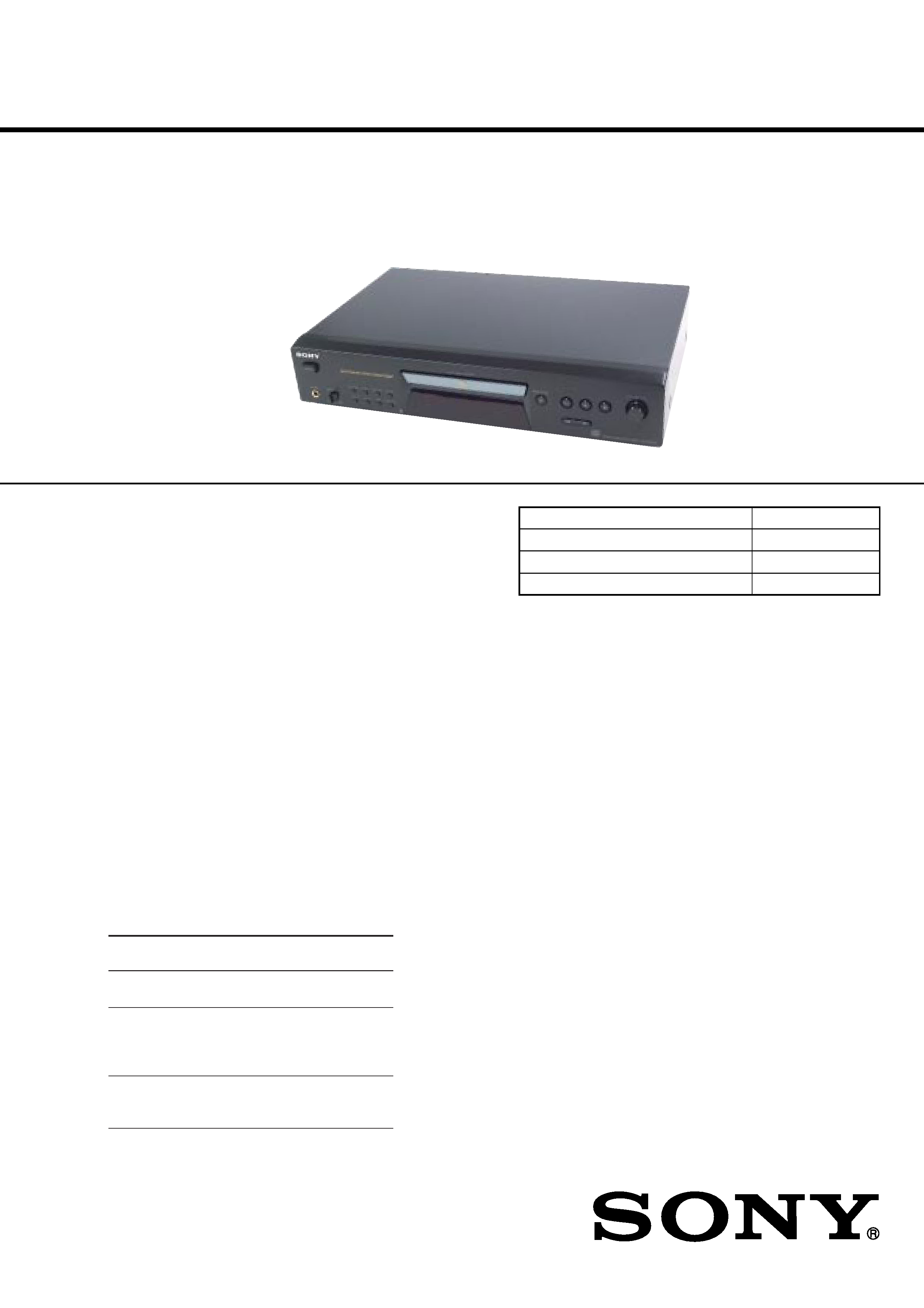
SCD-XE670
Ver 1.0 2001.07
SPECIFICATIONS
Model Name Using Similar Mechanism
NEW
CD Mechanism Type
CDM66B-DVBU6A
Base Unit Name
DVBU6A
Optical Pick-up Name
KHM-230AAA
9-873-176-01
Sony Corporation
2001G0500-1
Home Audio Company
C
2001.7
Shinagawa Tec Service Manual Production Group
When a super audio CD is played
Playing frequency range
2 Hz to 100 kHz
Frequency response
2 Hz to 50 kHz (3 dB)
Dynamic range
103 dB or more
Total harmonic distortion
rate
0.0020 % or less
Wow and flutter
Value of measurable limit
(
±0.001 % W. PEAK) or
less
When a CD is played
Frequency response
2 Hz to 20 kHz
Dynamic range
98 dB or more
Total harmonic distortion
rate
0.0025 % or less
Wow and flutter
Value of measurable limit
(
±0.001 % W. PEAK) or
less
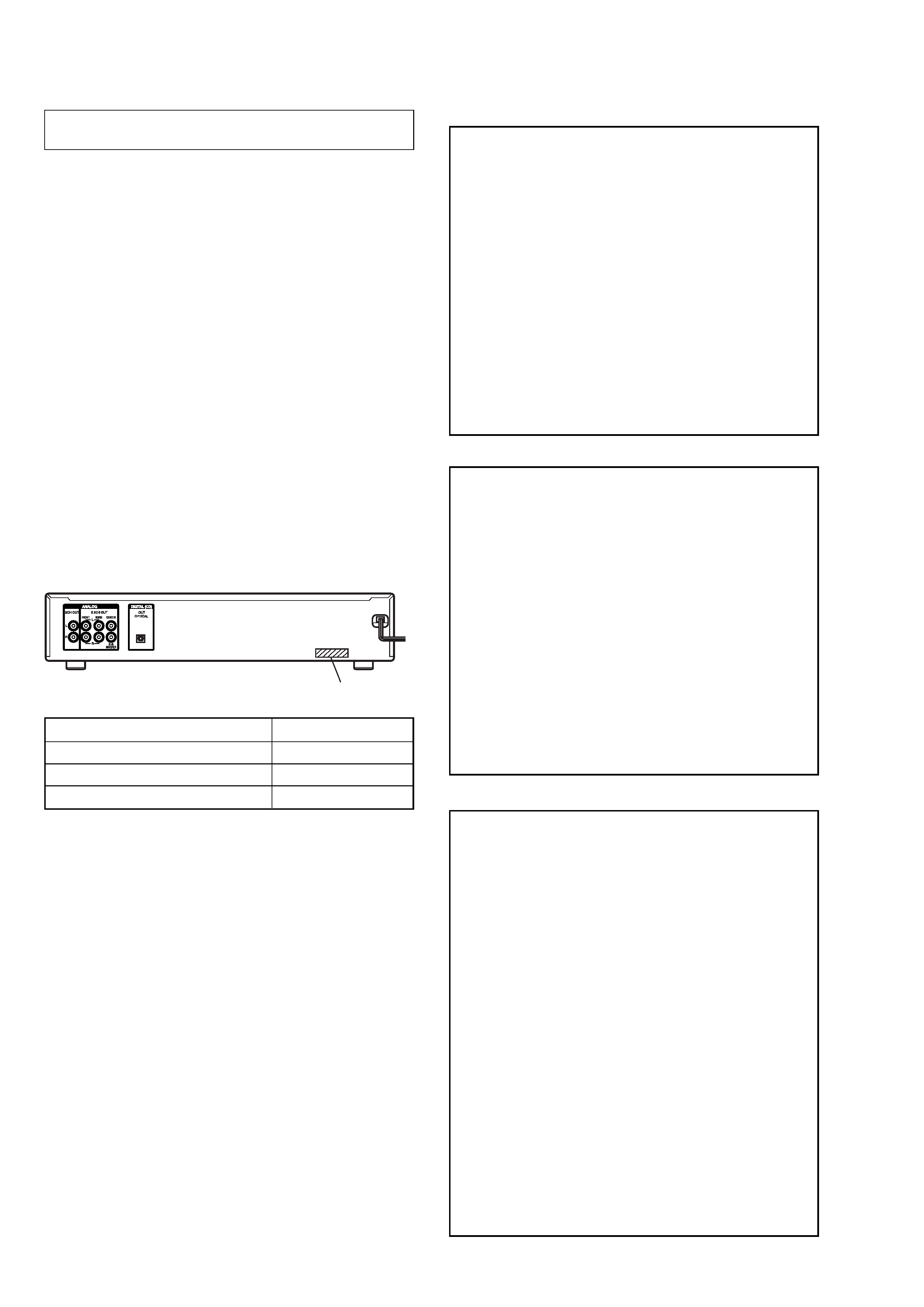
Output connector
ANALOG
OUT
DIGITAL
(CD) OUT
OPTICAL *
PHONES
*Output only the audio signals of the CD
Load
impedance
Over 10
kilohms
Wave
length:
660 nm
32 ohms
Jack
type
Phono
jacks
Square
optical
output
connector
Stereo
phone
jack
Output level
2 Vrms
(at 50 kilohms)
18 dBm
10 mW
General
Laser:
Semiconductor laser
(SACD:
= 650 nm)
(CD:
= 780 nm)
Emission duration: continuous
Power requirements
120 V AC, 60 Hz
Power consumption
26 W
Dimensions (w/h/d)
430
× 95 × 285 mm
(w/h/d)
(17 x 3 3/4 x 11 1/4 in.)
incl. projecting parts
Mass (approx.)
3.9 kg (9 lbs 5 oz)
Supplied accessories
Design and specifications are subject to change
without notice.
This player comes with the following items:
· Audio connecting cord
phono jack
× 2 (Red and White) y phono
jack
× 2 (Red and White) (2)
phono jack
× 1 (Black) y phono jack × 1
(Black) (2)
· Remote commander RM-SX700 (1)
· Size AA (R6) batteries (2)

2
SCD-XE670
TABLE OF CONTENTS
1.
SERVICING NOTES ............................................... 4
2.
GENERAL ................................................................... 6
3.
DISASSEMBLY
3-1. Disassembly Flow ...........................................................
8
3-2. Case (408226) .................................................................
9
3-3. Front Panel Section .........................................................
9
3-4. AUDIO Board, MAIN Board .......................................... 10
3-5. Mechanism Deck (CDM66B-DVBU6A) ....................... 10
3-6. Base Unit (DVBU6A) ..................................................... 11
4.
TEST MODE .............................................................. 12
5.
DIAGRAMS
5-1. Block Diagram RF/SERVO Section ........................ 26
5-2. Block Diagram SERVO Section .............................. 27
5-3. Block Diagram MAIN Section ................................ 28
5-4. Block Diagram AUDIO Section .............................. 29
5-5. Block Diagram DISPLAY/KEY CONTROL/
POWER SUPPLY Section ........................................... 30
5-6. Note for Printed Wiring Boards and
Schematic Diagrams ....................................................... 31
5-7. Schematic Diagram RF Board ................................. 32
5-8. Printed Wiring Boards RF/LOADING Boards ....... 33
5-9. Printed Wiring Board
MAIN Board (Component Side) .............................. 34
5-10. Printed Wiring Board
MAIN Board (Conductor Side) ................................ 35
5-11. Schematic Diagram
MAIN (1/5)/LOADING Boards .............................. 36
5-12. Schematic Diagram MAIN Board (2/5) .................. 37
5-13. Schematic Diagram MAIN Board (3/5) .................. 38
5-14. Schematic Diagram MAIN Board (4/5) .................. 39
5-15. Schematic Diagram MAIN Board (5/5) .................. 40
5-16. Schematic Diagram
AUDIO/HEADPHONE Boards ................................ 41
5-17. Printed Wiring Board
AUDIO Board (Component Side) ............................ 42
5-18. Printed Wiring Boards AUDIO (Conductor Side)/
HEADPHONE Boards ................................................. 43
5-19. Printed Wiring Boards DISPLAY/KEY Boards ...... 44
5-20. Schematic Diagram DISPLAY/KEY Boards .......... 45
5-21. Printed Wiring Boards
POWER/POWER SW/PT Boards ............................ 46
5-22. Schematic Diagram
POWER/POWER SW/PT Boards ............................ 47
5-23. IC Pin Function Description ........................................... 55
6.
EXPLODED VIEWS
6-1. Case Section .................................................................... 70
6-2. Front Panel Section ......................................................... 71
6-3. Chassis Section ............................................................... 72
6-4. Mechanism Deck Section (CDM66B-DVBU6A) .......... 73
6-5. Base Unit Section (DVBU6A) ........................................ 74
7.
ELECTRICAL PARTS LIST ............................... 75
3
SCD-XE670
This label is located on the LEFT exterior.
Notes on chip component replacement
· Never reuse a disconnected chip component.
· Notice that the minus side of a tantalum capacitor may be dam-
aged by heat.
Flexible Circuit Board Repairing
· Keep the temperature of the soldering iron around 270 °C dur-
ing repairing.
· Do not touch the soldering iron on the same conductor of the
circuit board (within 3 times).
· Be careful not to apply force on the conductor when soldering
or unsoldering.
CAUTION
Use of controls or adjustments or performance of procedures
other than those specified herein may result in hazardous ra-
diation exposure.
SAFETY CHECK-OUT
After correcting the original service problem, perform the follow-
ing safety check before releasing the set to the customer:
Check the antenna terminals, metal trim, "metallized" knobs,
screws, and all other exposed metal parts for AC leakage.
Check leakage as described below.
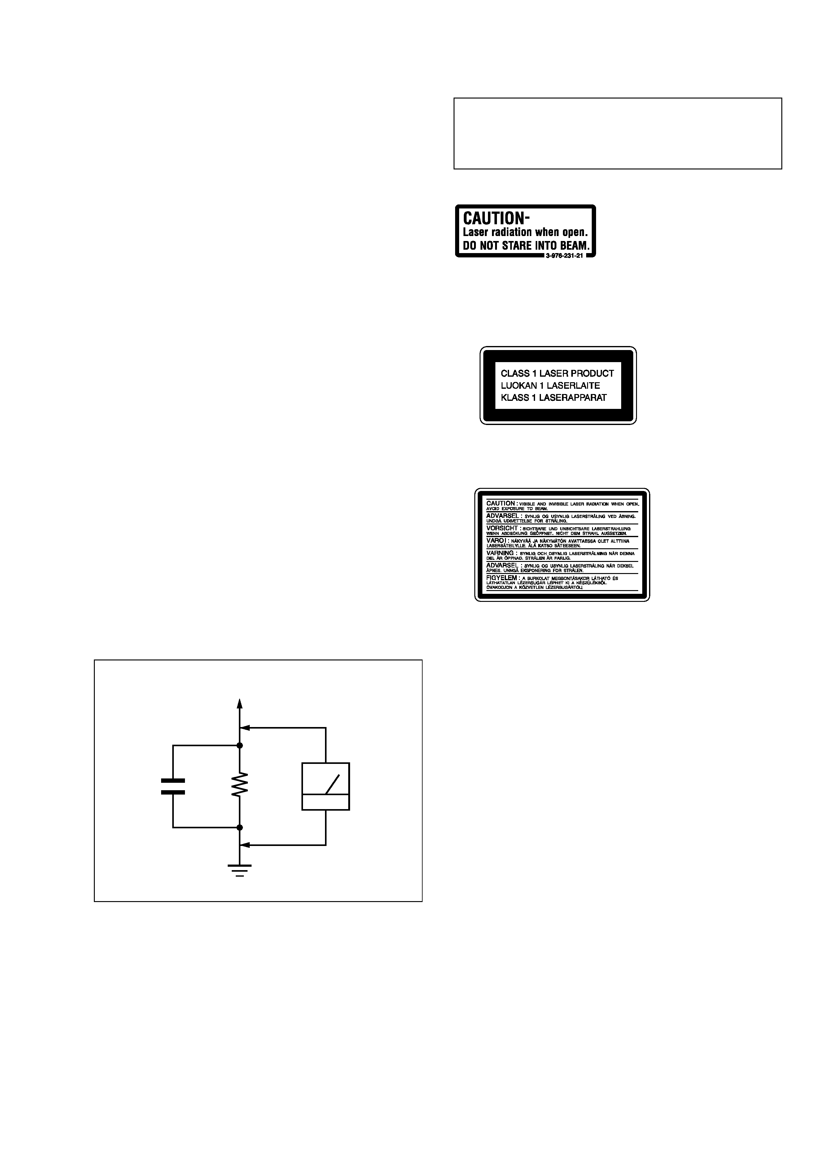
LEAKAGE TEST
The AC leakage from any exposed metal part to earth ground and
from all exposed metal parts to any exposed metal part having a
return to chassis, must not exceed 0.5 mA (500 microamperes.).
Leakage current can be measured by any one of three methods.
1. A commercial leakage tester, such as the Simpson 229 or RCA
WT-540A. Follow the manufacturers' instructions to use these
instruments.
2. A battery-operated AC milliammeter. The Data Precision 245
digital multimeter is suitable for this job.
3. Measuring the voltage drop across a resistor by means of a
VOM or battery-operated AC voltmeter. The "limit" indica-
tion is 0.75 V, so analog meters must have an accurate low-
voltage scale. The Simpson 250 and Sanwa SH-63Trd are ex-
amples of a passive VOM that is suitable. Nearly all battery
operated digital multimeters that have a 2 V AC range are suit-
able. (See Fig. A)
Fig. A.
Using an AC voltmeter to check AC leakage.
1.5 k
0.15
µF
AC
voltmeter
(0.75 V)
To Exposed Metal
Parts on Set
Earth Ground
ATTENTION AU COMPOSANT AYANT RAPPORT
À LA SÉCURITÉ!
LES COMPOSANTS IDENTIFIÉS PAR UNE MARQUE 0
SUR LES DIAGRAMMES SCHÉMATIQUES ET LA LISTE
DES PIÈCES SONT CRITIQUES POUR LA SÉCURITÉ
DE FONCTIONNEMENT. NE REMPLACER CES COM-
POSANTS QUE PAR DES PIÈCES SONY DONT LES
NUMÉROS SONT DONNÉS DANS CE MANUEL OU
DANS LES SUPPLÉMENTS PUBLIÉS PAR SONY.
SAFETY-RELATED COMPONENT WARNING!!
COMPONENTS IDENTIFIED BY MARK 0 OR DOTTED
LINE WITH MARK 0 ON THE SCHEMATIC DIAGRAMS
AND IN THE PARTS LIST ARE CRITICAL TO SAFE
OPERATION. REPLACE THESE COMPONENTS WITH
SONY PARTS WHOSE PART NUMBERS APPEAR AS
SHOWN IN THIS MANUAL OR IN SUPPLEMENTS PUB-
LISHED BY SONY.
This appliance is classified as a CLASS 1
LASER product.
The CLASS 1 LASER PRODUCT
MARKING is located on the rear exterior.
The following caution label is located
inside the unit.
4
SCD-XE670
(1) CD
1.
Sled reverse move (sled in)
2.
Disc detect
3.
IC setting for CD
4.
Servo error signal offset auto adjustment
5.
Spindle kick for LD on
6.
LD on
7.
Focus search
8.
Focus servo on
9.
Spindle kick
10. Spindle servo on
11. E-F balance auto adjustment
12. Tracking & sled servo on
13. Focus bias auto adjustment
14. Focus servo gain auto adjustment
15. Tracking servo gain auto adjustment
16. Jump to lead-in area
17. Read TOC
18. Stop
(2) SACD (single layer)
1.
Sled reverse move (sled in)
2.
Disc detect
3.
IC setting for SACD
4.
Servo error signal offset auto adjustment
5.
Spindle kick for LD on
6.
LD on
7.
Focus search
8.
Focus servo on
9.
Spindle kick
10. Spindle servo on
11. E-F balance auto adjustment
12. Tracking & sled servo on
13. Focus bias auto adjustment
14. Focus servo gain auto adjustment
15. Tracking servo gain auto adjustment
16. Jump to lead-in area
17. Read TOC
18. Stop
(3) SACD (dual layer)
1.
Sled reverse move (sled in)
2.
Disc detect
3.
IC setting for SACD
4.
Servo error signal offset auto adjustment
5.
Spindle kick for LD on
6.
LD on
7.
Focus search
8.
Focus servo on (layer 0)
9.
Spindle kick
10. Spindle servo on
11. E-F balance auto adjustment (layer 0)
12. Tracking & sled servo on (layer 0)
13. Focus bias auto adjustment (layer 0)
14. Focus servo gain auto adjustment (layer 0)
15. Tracking servo gain auto adjustment (layer 0)
16. Jump to lead-in area
17. Read TOC
18. Focus jump (layer 0
tlayer 1)
19. E-F balance auto adjustment (layer 1)
20. Tracking & sled servo on (layer 1)
21. Focus bias auto adjustment (layer 1)
22. Focus servo gain auto adjustment (layer 1)
23. Tracking servo gain auto adjustment (layer 1)
24. Focus Jump (layer 1
tlayer 0)
25. Stop
SECTION 1
SERVICING NOTES
The laser diode in the optical pick-up block may suffer electro-
static break-down because of the potential difference generated
by the charged electrostatic load, etc. on clothing and the human
body.
During repair, pay attention to electrostatic break-down and also
use the procedure in the printed matter which is included in the
repair parts.
The flexible board is easily damaged and should be handled with
care.
NOTES ON LASER DIODE EMISSION CHECK
The laser beam on this model is concentrated so as to be focused
on the disc reflective surface by the objective lens in the optical
pick-up block. Therefore, when checking the laser diode emis-
sion, observe from more than 30 cm away from the objective lens.
CLEANING OF OPTICAL PICK-UP LENS
In cleaning the lens of optical pick-up, use the air blower.
Never use a cotton swab for cleaning the lens of optical pick-up,
which otherwise causes a trouble.
MODEL IDENTIFICATION
Rear Panel
RESETTING OPERATION AT POWER ON
If the power is turned on with a disc loaded in the set, a sequence
of operation as shown below will be performed.
(The operation varies depending on the type of disc)
Condition: continue mode
NOTES ON HANDLING THE OPTICAL PICK-UP
BLOCK OR BASE UNIT
PART No.
MODEL
PART No.
AEP and UK models
4-234-033-0[]
US model
4-234-033-2[]
Canadian model
4-234-033-4[]
5
SCD-XE670
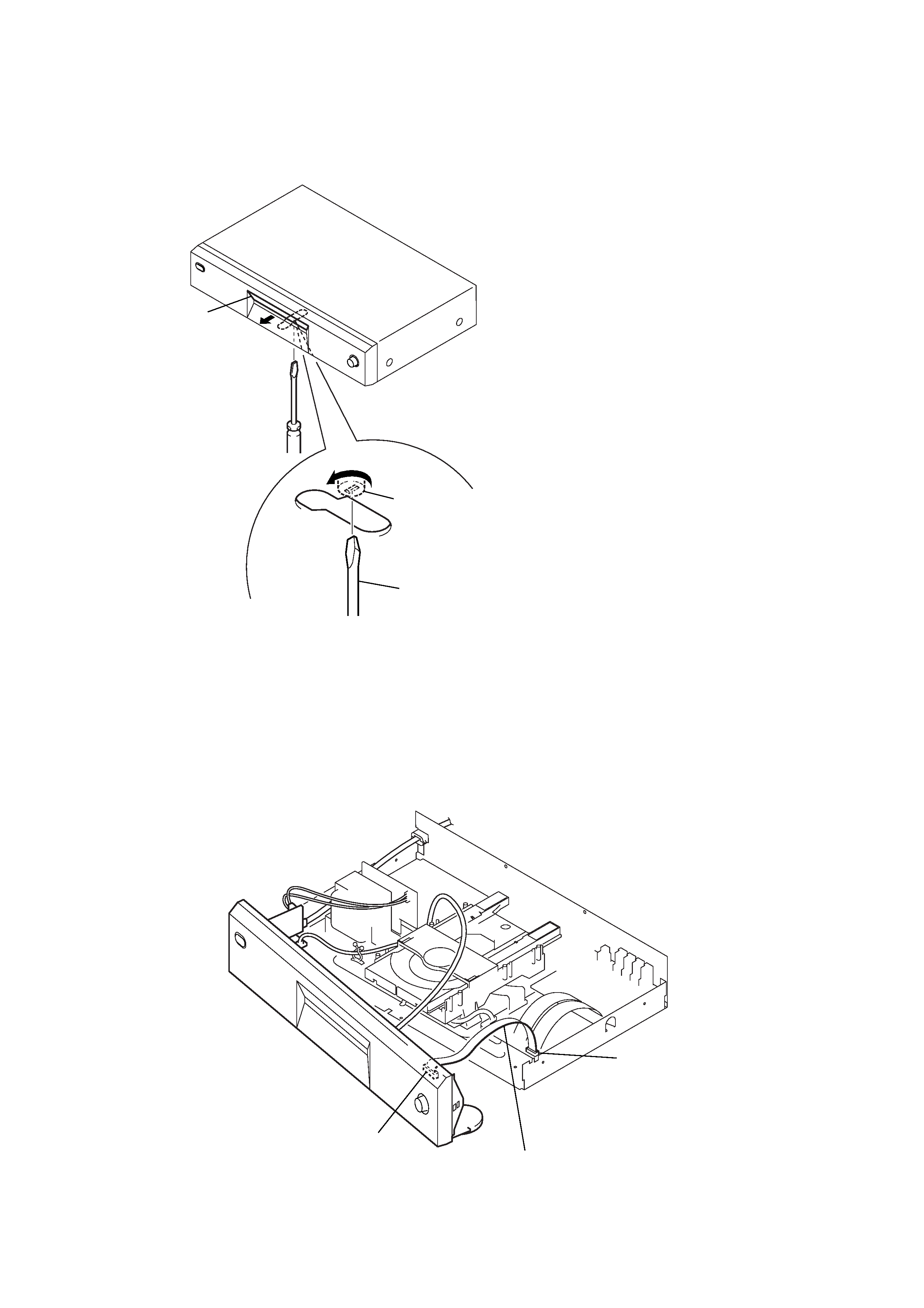
HOW TO OPEN THE TRAY WHEN POWER SWITCH TURNS OFF
DISPLAY BOARD SERVICE POSITION
In checking the DISPLAY board, prepare jig (extension cable J-8000-024-A : 1.00 mm Pitch, 12 cores, Length 300 mm.)
tray
tapering driver
cam (66)
1
Insert a tapering driver (3 mm in diameter)
in the hole at the bottom of the unit,
turn the cam (66) fully in the direction of arrow A.
A
MAIN board
(CN706)
DISPLAY board
(CN801)
Connect jig (extension cable J-8000-024-A)
to the DISPLAY board (CN801) and
MAIN board (CN706).