
SERVICE MANUAL
US Model
Canadian Model
AEP Model
SCD-1/777ES
3.
SERVICING NOTES ............................................... 3
4.
DISASSEMBLY-2 ..................................................... 5
5.
TEST MODE .............................................................. 10
6.
ELECTRICAL ADJUSTMENTS ......................... 12
7.
DIAGRAMS
7-1. Notes for Printed Wiring Board and
Schematic Diagram ......................................................... 17
7-2. Printed Wiring Boards RF/SLD-FG/SLD-MOT
Boards ........................................................................... 18
7-3. Schematic Diagram RF/SLD-FG/SLD-MOT
Boards ........................................................................... 19
7-4. Printed Wiring Boards LOAD-CN/LOAD-MOT/
LOAD-SW/STB Boards .............................................. 20
7-5. Schematic Diagram LOAD-CN/LOAD-MOT/
LOAD-SW/STB Boards .............................................. 21
7-6. Printed Wiring Board MAIN Board
(component side) .......................................................... 22
7-7. Printed Wiring Board MAIN Board
(conductor side) ........................................................... 23
7-8. Schematic Diagram MAIN Board (1/7) .................. 24
7-9. Schematic Diagram MAIN Board (2/7) .................. 25
7-10. Schematic Diagram MAIN Board (3/7) .................. 26
7-11. Schematic Diagram MAIN Board (4/7) .................. 27
7-12. Schematic Diagram MAIN Board (5/7) .................. 28
7-13. Schematic Diagram MAIN Board (6/7) .................. 29
7-14. Schematic Diagram MAIN Board (7/7) .................. 30
7-15. Printed Wiring Board AUDIO Board ...................... 31
7-16. Schematic Diagram AUDIO Board (1/2) ................ 32
7-17. Schematic Diagram AUDIO Board (2/2) ................ 33
7-18. Printed Wiring Boards BAL(SCD-1)/COAX/
OPT/PIN/SW Boards ................................................... 34
7-19. Schematic Diagram BAL(SCD-1)/COAX/
OPT/PIN/SW Boards ................................................... 35
7-20. Printed Wiring Boards DISPLAY/SW-L/
SW-R Boards ................................................................ 36
7-21. Schematic Diagram DISPLAY/SW-L/
SW-R Boards ................................................................ 37
7-22. Printed Wiring Boards AC/POWER Boards ........... 38
7-23. Schematic Diagram AC/POWER Boards ................ 39
7-24. IC Pin Function Description ........................................... 43
8.
EXPLODED VIEWS ................................................ 50
9.
ELECTRICAL PARTS LIST ............................... 59
TABLE OF CONTENTS
2
Notes on chip component replacement
· Never reuse a disconnected chip component.
· Notice that the minus side of a tantalum capacitor may be dam-
aged by heat.
Flexible Circuit Board Repairing
· Keep the temperature of the soldering iron around 270 °C dur-
ing repairing.
· Do not touch the soldering iron on the same conductor of the
circuit board (within 3 times).
· Be careful not to apply force on the conductor when soldering
or unsoldering.
ATTENTION AU COMPOSANT AYANT RAPPORT
À LA SÉCURITÉ!
LES COMPOSANTS IDENTIFIÉS PAR UNE MARQUE 0
SUR LES DIAGRAMMES SCHÉMATIQUES ET LA LISTE
DES PIÈCES SONT CRITIQUES POUR LA SÉCURITÉ
DE FONCTIONNEMENT. NE REMPLACER CES COM-
POSANTS QUE PAR DES PIÈCES SONY DONT LES
NUMÉROS SONT DONNÉS DANS CE MANUEL OU
DANS LES SUPPLÉMENTS PUBLIÉS PAR SONY.
SAFETY-RELATED COMPONENT WARNING!!
COMPONENTS IDENTIFIED BY MARK 0 OR DOTTED
LINE WITH MARK 0 ON THE SCHEMATIC DIAGRAMS
AND IN THE PARTS LIST ARE CRITICAL TO SAFE
OPERATION. REPLACE THESE COMPONENTS WITH
SONY PARTS WHOSE PART NUMBERS APPEAR AS
SHOWN IN THIS MANUAL OR IN SUPPLEMENTS PUB-
LISHED BY SONY.
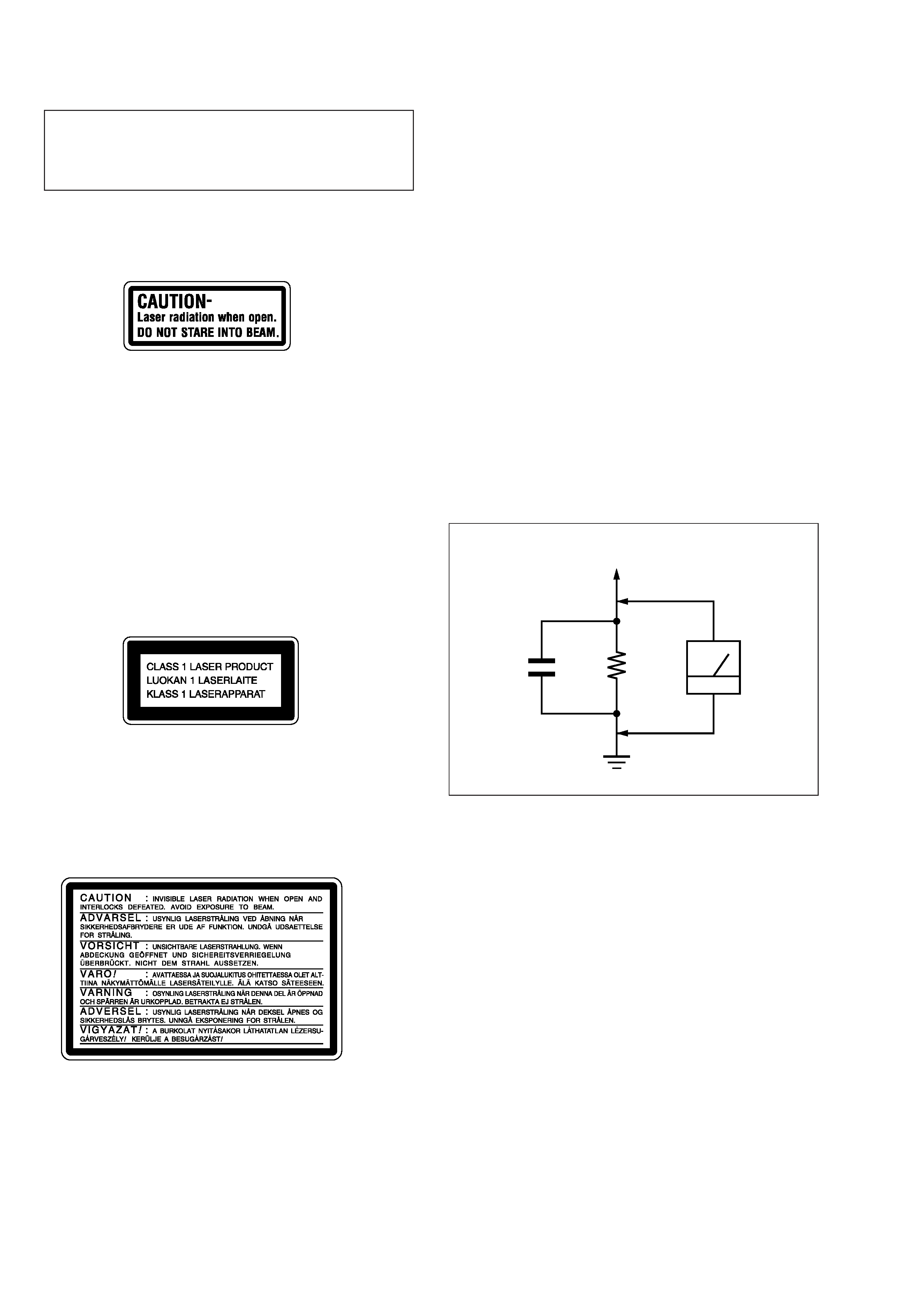
CAUTION
Use of controls or adjustments or performance of procedures
other than those specified herein may result in hazardous ra-
diation exposure.
Laser component in this product is capable of emitting radiation
exceeding the limit for Class 1.
The following caution label is located inside the unit.
SAFETY CHECK-OUT
After correcting the original service problem, perform the follow-
ing safety check before releasing the set to the customer:
Check the antenna terminals, metal trim, "metallized" knobs,
screws, and all other exposed metal parts for AC leakage.
Check leakage as described below.
LEAKAGE TEST
The AC leakage from any exposed metal part to earth ground and
from all exposed metal parts to any exposed metal part having a
return to chassis, must not exceed 0.5 mA (500 microamperes.).
Leakage current can be measured by any one of three methods.
1. A commercial leakage tester, such as the Simpson 229 or RCA
WT-540A. Follow the manufacturers' instructions to use these
instruments.
2. A battery-operated AC milliammeter. The Data Precision 245
digital multimeter is suitable for this job.
3. Measuring the voltage drop across a resistor by means of a
VOM or battery-operated AC voltmeter. The "limit" indica-
tion is 0.75 V, so analog meters must have an accurate low-
voltage scale. The Simpson 250 and Sanwa SH-63Trd are ex-
amples of a passive VOM that is suitable. Nearly all battery
operated digital multimeters that have a 2 V AC range are suit-
able. (See Fig. A)
1.5 k
0.15
µF
AC
voltmeter
(0.75 V)
To Exposed Metal
Parts on Set
Earth Ground
The following caution label is located
inside of the unit.
For the customers in Canada
CAUTION
TO PREVENT ELECTRIC SHOCK, DO
NOT USE THIS POLARIZED AC PLUG
WITH AN EXTENSION CORD,
RECEPTACLE OR OTHER OUTLET
UNLESS THE BLADES CAN BE FULLY
INSERTED TO PREVENT BLADE
EXPOSURE.
For the customers in Europe
This appliance is classified as a CLASS 1
LASER product.
The CLASS 1 LASER PRODUCT
MARKING is located on the rear exterior.
Fig. A.
Using an AC voltmeter to check AC leakage.
3
SECTION 3
SERVICING NOTES
The laser diode in the optical pick-up block may suffer electro-
static break-down because of the potential difference generated
by the charged electrostatic load, etc. on clothing and the human
body.
During repair, pay attention to electrostatic break-down and also
use the procedure in the printed matter which is included in the
repair parts.
The flexible board is easily damaged and should be handled with
care.
NOTES ON LASER DIODE EMISSION CHECK
The laser beam on this model is concentrated so as to be focused
on the disc reflective surface by the objective lens in the optical
pick-up block. Therefore, when checking the laser diode emis-
sion, observe from more than 30 cm away from the objective lens.
MODEL IDENTIFICATION
NOTES ON HANDLING THE OPTICAL PICK-UP
BLOCK OR BASE UNIT
Part No.
Back Panel
Model
Part No.
SCD-1: US, Canadian
4-215-784-1s
SCD-1: AEP
4-215-784-2s
SCD-777ES: AEP
4-221-854-0s
SCD-777ES: US, Canadian
4-221-854-1s
CHECKING METHOD OF MICROCOMPUTER ROM
VERSION
1. Set the CD1/CD2 switch on the remote commander to CD1.
2. With the power turned on, press the [CHECK] button on the
remote commander while pressing the [TEXT] button on the
set.
3. 15-digit numeric value will be displayed, and the top 4 digits
(left side) of the numeric value imply the microcomputer ROM
version.
Example: If "200006100FFFF3C" is displayed, the ROM ver-
sion is 2.000.
4. To cancel the ROM version check mode, press the [CHECK]
button on the remote commander while pressing the [TEXT]
button on the set.
DISPLAY OF TOC ERROR
insulator
OP mechanism section (BU-23)
Any board to put
connect two jigs (extension cable J-2501-164-A) to the RF board
(CN001, 002) and Main board (CN501, 502).
SERVICE POSITION
In checking the BU section, prepare two new jigs (extension cable J-2501-164-A: 1.00 mm 26 cores).
Display
Contents
TOC ERROR **** Illegal SACD disc (pirate edition)
TOC ERROR *
Not SACD (DVD disc etc.)
4
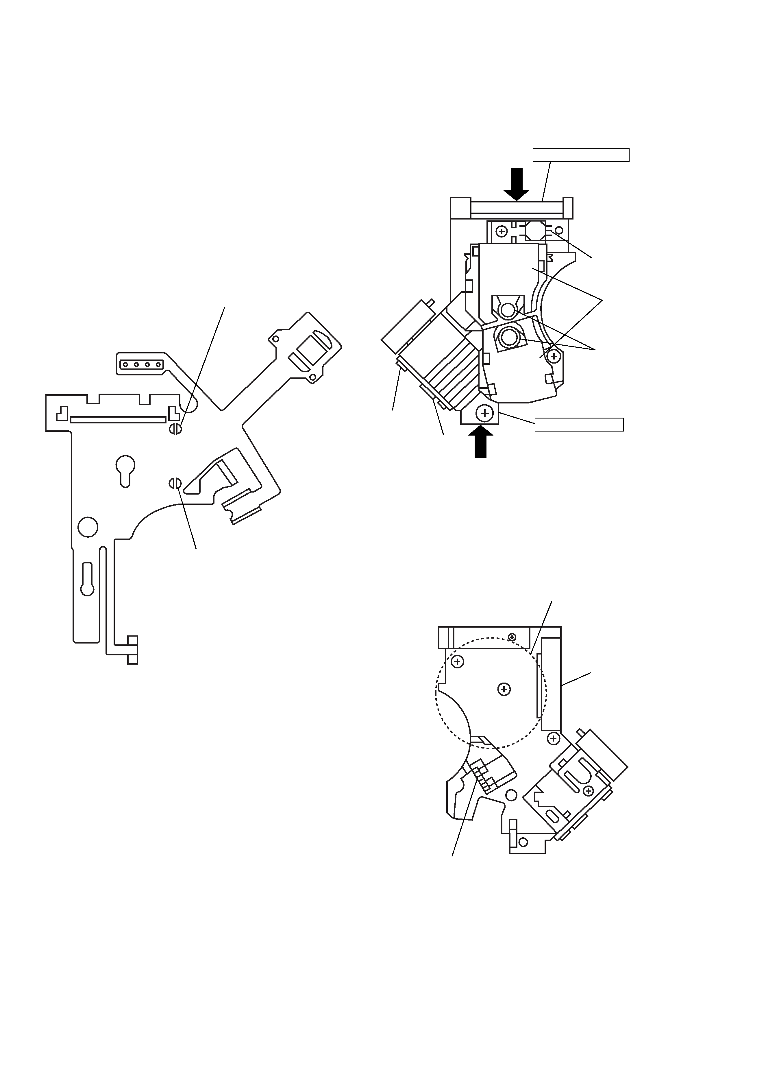
REPLACING OPTICAL PICK-UP
Handling
1) A red laser diode for Super Audio CD Player requires more
attention to static electricity than general infrared laser diodes
for CD.
Because its durability to static electricity is far weaker than
that of infrared laser diodes, always use an earth band when
handling the optical pick-up block as service parts.
2) As for the flexible board KHS-180A (RP) packed as service
parts, the short lands have been soldered to protect from static
electricity. Accordingly, remove solders when replacing opti-
cal pick-up. (See Fig. 1)
Fig. 1 Flexible board
3) In handling the KHS-180A (RP), do not touch inhibited parts
shown in Fig. 2, but grip the slide base bearing and U-shaped
guide.
Fig. 2 KHS-180A (RP)
DVD short land
CD short land
Slide base bearing
Skew sensor
Lens actuator
covers
Objective lenses
U-shaped guide
OEIC
Laser holder
Flexible board
Connector
Laser coupler
Touch inhibited parts
· Objective lens
· Skew sensor
· Laser holder
· Laser coupler
· Flexible board
· OEIC
· Lens actuator covers
5
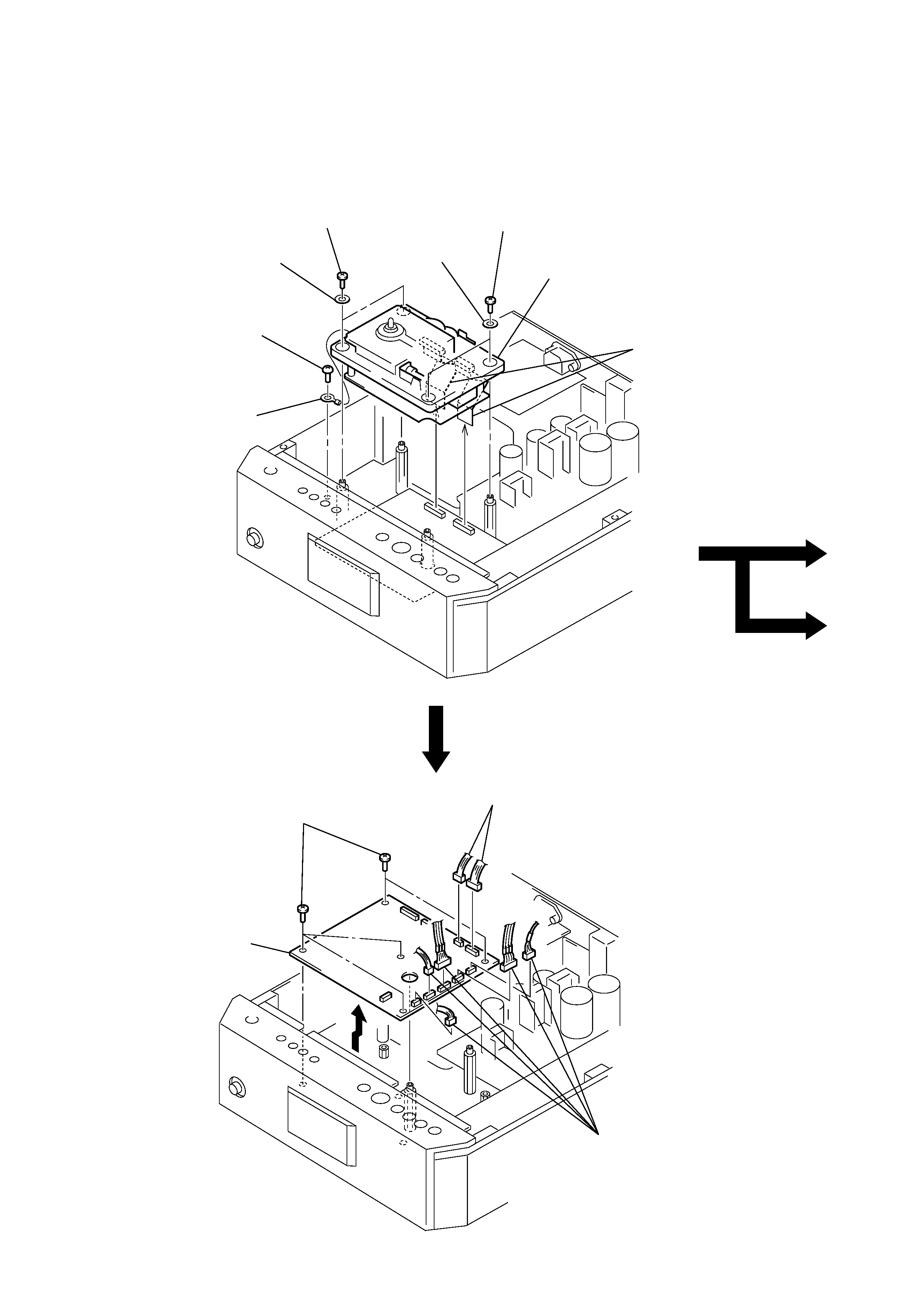
OP MECHANISM SECTION (BU-23)
MAIN BOARD
Note: Follow the disassembly procedure in the numerical order given.
SECTION 4
DISASSEMBLY-2
2
five screws
(PS 3
× 5)
1
two connectors
(CN701, 708)
1
five connectors
(CN702-706)
3
MAIN board
OPTICAL PICK-UP
(KHS-180A/J1N) (Page 7)
RF BOARD (Page 7)
2
lag
1
screw (PS3
× 5)
4
two washers
4
two washers
3
two screws
(B2.6
× 5)
3
two screws
(B2.6
× 5)
5
Lift up OP mechanism section (BU-23).
6
two wires (flat type) (26 core)
(CN501, 502)