MICROFILM
SERVICE MANUAL
PERSONAL
MINIDISC SYSTEM
US Model
CD
Model Name Using Similar Mechanism
NEW
Section
CD Mechanism Type
KSM-213CGP
Optical Pick-up Name
KSS-213C
MD
Model Name Using Similar Mechanism
MDS-JB920
Section
MD Mechanism Type
MDM-5A
Base Unit Name
MBU-5A
Optical Pick-up Name
KMS-260A
SPECIFICATIONS
PMC-MD55
U.S. and foreign patents licensed form Dolby Laboratories
Licensing Corporation.
Ver 1.0 1999. 06

2
1.
SERVICING NOTES ..............................................
3
2.
GENERAL
Playing a CD ..................................................................
6
Recording a Whole CD ..................................................
6
Playing an MD ...............................................................
7
Listening to the radio .....................................................
7
Setting the Clock ............................................................
8
Hooking up the System ..................................................
8
3.
DISASSEMBLY ........................................................
9
4.
TEST MODE ............................................................. 15
5.
ELECTRICAL ADJUSTMENTS
Tuner Section ................................................................. 20
MD Section .................................................................... 21
CD Section ..................................................................... 28
Display Section .............................................................. 30
6.
DIAGRAMS
6-1. Block Diagram TUNER Section ............................ 31
6-2
Block Diagram MD Section ................................... 34
6-3. Block Diagram CD Section .................................... 37
6-4. Block Diagram
FUNCTION SELECT/PANEL Section ................... 40
6-5. Block Diagram
POWER AMP/POWER SUPPLY Section .............. 43
6-6. Block Diagram SUPER WOOFER Section ........... 45
6-7. Printed Wiring Board TUNER Section .................. 49
6-8. Schematic Diagram TUNER Section ..................... 51
6-9. Schematic Diagram BD Section ............................. 53
6-10. Printed Wiring Boards BD Section ........................ 57
6-11. Printed Wiring Board DG Section .......................... 59
6-12. Schematic Diagram DG Section ............................. 61
SAFETY-RELATED COMPONENT WARNING!!
COMPONENTS IDENTIFIED BY MARK
! OR DOTTED
LINE WITH MARK
! ON THE SCHEMATIC DIAGRAMS
AND IN THE PARTS LIST ARE CRITICAL TO SAFE
OPERATION. REPLACE THESE COMPONENTS WITH
SONY PARTS WHOSE PART NUMBERS APPEAR AS
SHOWN IN THIS MANUAL OR IN SUPPLEMENTS PUB-
LISHED BY SONY.
CAUTION
Use of controls or adjustments or performance of procedures
other than those specified herein may result in hazardous ra-
diation exposure.
This appliance is classified as a CLASS 1 LASER product.
The CLASS 1 LASER PRODUCT MARKING is located on
the rear exterior.
Laser component in this product is capable of emitting radiation
exceeding the limit for Class 1.
TABLE OF CONTENTS
6-13. Printed Wiring Boards MAIN Section ................... 64
6-14. Schematic Diagram MAIN (CD) Section .............. 67
6-15. Schematic Diagram
MAIN (SYSTEM CONTROL) Section .................. 70
6-16. Schematic Diagram
MAIN (FUNCTION SELECT) Section .................. 73
6-17. Printed Wiring Board AUDIO/JACK Section ........ 75
6-18. Schematic Diagram AUDIO/JACK Section .......... 77
6-19. Schematic Diagram CD MOTOR Section ............. 79
6-20. Printed Wiring Board CD MOTOR Section .......... 81
6-21. Printed Wiring Board
CD OPEN/CLOSE Section ...................................... 82
6-22. Schematic Diagram CD OPEN/CLOSE Section ... 83
6-23. Printed Wiring Boards PANEL Section ................. 86
6-24. Schematic Diagram PANEL Section ...................... 89
6-25. Printed Wiring Boards
POWER AMP/POWER Section .............................. 91
6-26. Schematic Diagram
POWER AMP/POWER Section .............................. 93
6-27. Printed Wiring Boards
SUPER WOOFER Section ...................................... 95
6-28. Schematic Diagram
SUPER WOOFER Section ...................................... 97
6-29. IC Pin Function Description .......................................... 108
7.
EXPLODED VIEWS ............................................... 118
8.
ELECTRICAL PARTS LIST .............................. 128
3
SECTION 1
SERVICING NOTES
SAFETY CHECK-OUT
After correcting the original service problem, perform the follow-
ing safety check before releasing the set to the customer:
Check the antenna terminals, metal trim, "metallized" knobs,
screws, and all other exposed metal parts for AC leakage.
Check leakage as described below.
LEAKAGE TEST
The AC leakage from any exposed metal part to earth ground and
from all exposed metal parts to any exposed metal part having a
return to chassis, must not exceed 0.5 mA (500 microamperes).
Leakage current can be measured by any one of three methods.
1. A commercial leakage tester, such as the Simpson 229 or RCA
WT-540A. Follow the manufacturers' instructions to use these
instruments.
2. A battery-operated AC milliammeter. The Data Precision 245
digital multimeter is suitable for this job.
3. Measuring the voltage drop across a resistor by means of a
VOM or battery-operated AC voltmeter. The "limit" indica-
tion is 0.75 V, so analog meters must have an accurate low-
voltage scale. The Simpson 250 and Sanwa SH-63Trd are ex-
amples of a passive VOM that is suitable. Nearly all battery
operated digital multimeters that have a 2 V AC range are suit-
able. (See Fig. A)
Fig. A.
Using an AC voltmeter to check AC leakage.
1.5 k
0.15
µF
AC
voltmeter
(0.75 V)
To Exposed Metal
Parts on Set
Earth Ground
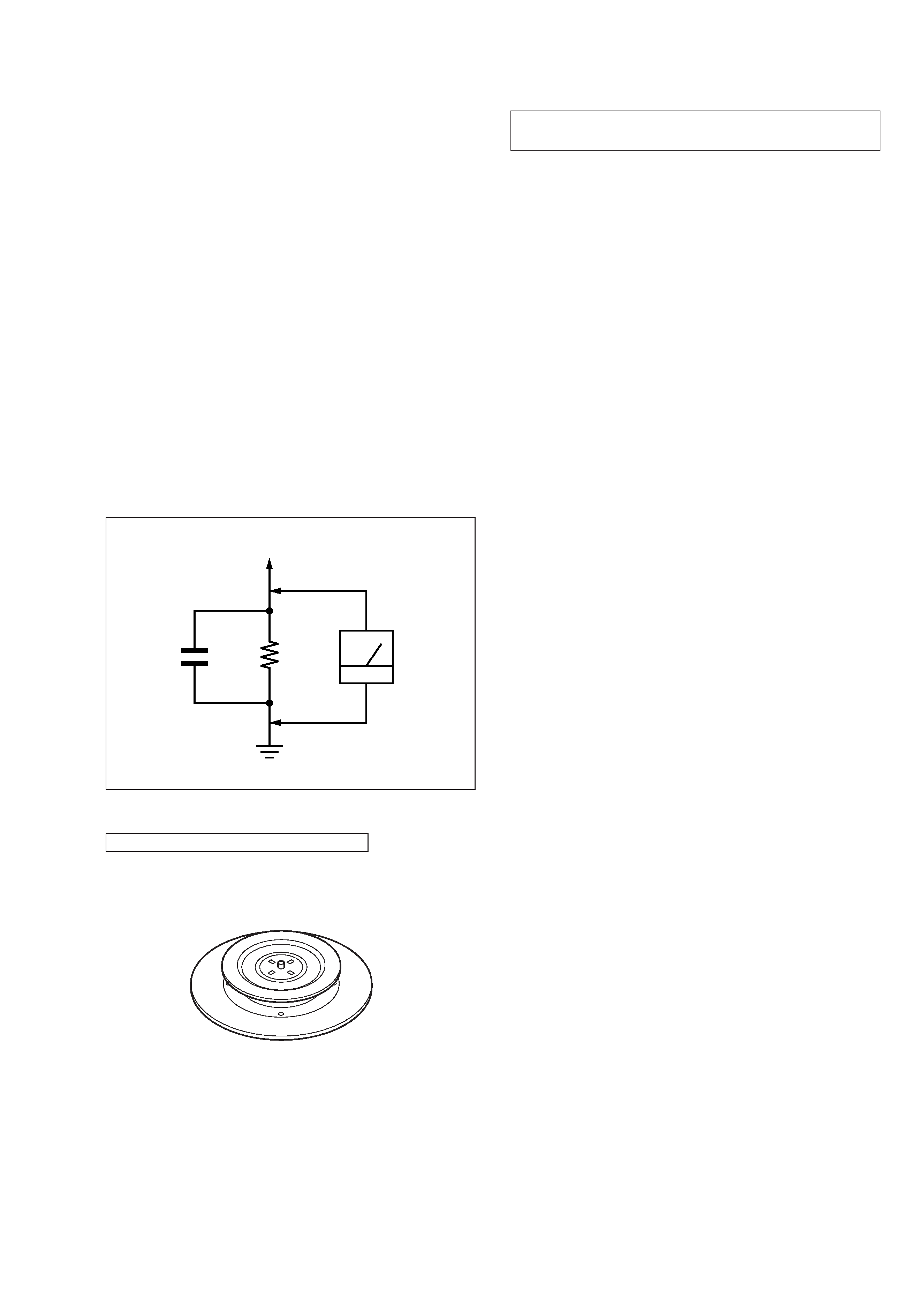
CHUCK PLATE JIG ON REPAIRING
On repairing CD section, playing a disc without the CD lid, use
Chuck Plate Jig.
· Code number of Chuck Plate Jig: X-4918-255-1
The laser diode in the optical pick-up block may suffer electro-
static break-down because of the potential difference generated
by the charged electrostatic load, etc. on clothing and the human
body.
During repair, pay attention to electrostatic break-down and also
use the procedure in the printed matter which is included in the
repair parts.
The flexible board is easily damaged and should be handled with
care.
NOTES ON LASER DIODE EMISSION CHECK
The laser beam on this model is concentrated so as to be focused
on the disc reflective surface by the objective lens in the optical
pick-up block. Therefore, when checking the laser diode emis-
sion, observe from more than 30 cm away from the objective lens.
Notes on chip component replacement
· Never reuse a disconnected chip component.
· Notice that the minus side of a tantalum capacitor may be dam-
aged by heat.
Flexible Circuit Board Repairing
· Keep the temperature of the soldering iron around 270 °C dur-
ing repairing.
· Do not touch the soldering iron on the same conductor of the
circuit board (within 3 times).
· Be careful not to apply force on the conductor when soldering
or unsoldering.
NOTES ON HANDLING THE OPTICAL PICK-UP
BLOCK OR BASE UNIT
4
JIG FOR CHECKING BD BOARD WAVEFORM
The special jig (J-2501-149-A) is useful for checking the waveform of the BD board. The names of terminals and the checking items to be
performed are shown as follows.
GND : Ground
I+3V : For measuring IOP (Check the deterioration of the optical pick-up laser)
IOP : For measuring IOP (Check the deterioration of the optical pick-up laser)
TEO : TRK error signal (Traverse adjustment)
VC
: Reference level for checking the signal
RF
: RF signal (Check jitter)
RF
VC
TEO
for MDM-5
IOP
I+3V
VC
RF
TEO
IOP
I+3V
GND
VC
RF
TEO
IOP
I+3V
GND
1
5
1
6
for MDM-3
CN110
RF
5P Connector
6P connector
VC
TEO
IOP
I+3V
GND
Mechanism deck

5
CHECKS PRIOR TO PARTS REPLACEMENT AND ADJUSTMENTS (for MD Section)
Before performing repairs, perform the following checks to determine the faulty locations up to a certain extent.
Details of the procedures are described in "5 Electrical Adjustments".
· 0.9 mW power
Specified value : 0.84 to 0.92 mW
· 7.0 mW power
Specified value : 6.8 to 7.2 mW
lop (at 7mW)
· Labeled on the optical pickup
Iop value ± 10mA
· Error rate check
Specified value : For points a, b, and c
C1 error : About 200
ADER : Below 2
· Error rate check
Specified value:
a.
When using test disc (MDW-74/AU-1)
C1 error : Below 80
ADER : Below 2
b.
When using check disc (TDYS-1)
C1 error : Below 50
· CPLAY error rate check
Specified value:
C1 error : Below 80
ADER : Below 2
Laser power check
(6-1 : See page 23)
Focus bias check
(6-2 : See page 23)
C PLAY check
(6-3 : See page 23)
Self-recording/playback
check
(6-4 : See page 23)
Criteria for Determination
(Unsatisfactory if specified value is not satisfied)
· Clean the optical pick-up
· Adjust again
· Replace the optical pick-up
· Replace the optical pick-up
· Replace the optical pick-up
· Replace the optical pick-up
If always unsatisfactory:
· Replace the overwrite head
· Check for disconnection of the circuits around the
overwrite head
If occasionally unsatisfactory:
· Check if the overwrite head is distorted
· Check the mechanism around the sled
Measure if unsatisfactory:
Note:
The criteria for determination above is intended merely to determine if satisfactory or not, and does not serve as the specified value for
adjustments.
When performing adjustments, use the specified values for adjustments.