PEG-S300,S300/HK
PERSONAL ENTERTAINMENT
ORGANIZER
9-928-164-32
This Board Repair describes IC pin function, block diagrams,
printed wiring boards, schematic diagrams, adjustments,
operation check and electrical parts list.
For other information, refer to the separate Service Manual.
TABLE OF CONTENTS
1. IC PIN FUNCTION ·························································· 3
2. BLOCK DIAGRAM ·························································· 5
3. PRINTED WIRING BOARDS AND
SCHEMATIC DIAGRAMS
· MP-23 (TOUCH PAD A/D CONVERTER)
SCHEMATIC DIAGRAM ................................................... 7
· MP-23 (DC-DC CONVERTER)
SCHEMATIC DIAGRAM ................................................... 9
· MP-23 (CPU) SCHEMATIC DIAGRAM ......................... 11
· MP-23 (ROM) SCHEMATIC DIAGRAM ........................ 13
· MP-23 (BUZZER) SCHEMATIC DIAGRAM ................. 15
· MP-23 (MEMORY STICK) SCHEMATIC DIAGRAM ... 17
· MP-23 (USB I/F) SCHEMATIC DIAGRAM ................... 19
· MP-23 (LCD CONTROL) SCHEMATIC DIAGRAM ..... 21
· MP-23 (MAIN) PRINTED WIRING BOARD ................. 23
· CNX-98 (BATTERY CHARGE)
PRINTED WIRING BOARD ............................................ 25
· CNX-98 (SWITCH) SCHEMATIC DIAGRAM ............... 27
· CNX-98 (POWER CONTROL)
SCHEMATIC DIAGRAM ................................................. 29
· CNX-98 (RS-232C DR/VER)
SCHEMATIC DIAGRAM ................................................. 31
4. ADJUSTMENTS
4-1. WRITING OS (OPERATING SYSTEM) ................... 33
4-2. USER ID WRITING ................................................... 33
4-3. DATA WRITING IN THE MEMORY STICK ........... 33
4-4. WRITING THE SMALLROM OF VER. RC1.8 ........ 34
4-5. USER ID WRITING (USING SERIAL CRADLE) ... 34
4-6. BIG ROM WRITING (USING USB CRADLE) ........ 34
4-7. REFURBISHING ........................................................ 34
5. OPERATION CHECK
5-1. INITIAL SETTING ..................................................... 35
5-2. EL BACKLIGHT OPERATION CHECK .................. 35
5-3. "CONTRAST ADJUSTMENT"
OPERATION CHECK ................................................ 35
5-4. MEMORY STICK OPERATION CHECK ................. 35
5-5. FRONT PANEL BUTTON OPERATION CHECK .... 35
5-6. INFRARED COMMUNICATION
OPERATION CHECK ................................................ 35
5-7. HOTSYNC FUNCTION OPERATION CHECK ....... 35
5-8. HARDWARE RESET ................................................. 35
6. ELECTRICAL PARTS LIST ······································· 36
SERVICE MANUAL
BOARD REPAIR
Contents other than "BOARD REPAIR" are shown
in the separate Service Manual (9-928-164-12).
US Model
Hong Kong Model
Illust : PEG-S300
Ver 2-2001A
All the supplementary
information are attached
at the end of data files.
Information in this document is subject to change without notice.
Sony and VAIO are trademarks of Sony. Intel logo and Intel Inside
logo are registered trademarks of Intel Corporation. Pentium MMX
is a trademark of Intel Corporation. Microsoft, MS-DOS, Windows,
the Windows 95 and Windows 98 logo are trademarks of Microsoft
Corporation.
All other trademarks are trademarks or registered trademarks of
their respective owners. Other trademarks and trade names may be
used in this document to refer to the entitles claiming the marks and
names or their produces. Sony Corporation disclaims any proprietary
interest in trademarks and trade names other than its own.
Service and Inspection Precautions
1. Obey precautionary markings and instructions
Labels and stamps on the cabinet, chassis, and components identify areas
requiring special precautions. Be sure to observe these precautions, as well
as all precautions listed in the operating manual and other associated
documents.
2. Use designated parts only
The set's components possess important safety characteristics, such as
noncombustibility and the ability to tolerate large voltages. Be sure that
replacement parts possess the same safety characteristics as the originals.
Also remember that the 0 mark, which appears in circuit diagrams and
parts lists, denotes components that have particularly important safety
functions; be extra sure to use only the designated components.
3. Always follow the original design when mounting
parts and routing wires
The original layout includes various safety features, such as inclusion of
insulating materials (tubes and tape) and the mounting of parts above the
printer board. In addition, internal wiring has been routed and clamped so
as to keep it away from hot or high-voltage parts. When mounting parts or
routing wires, therefore, be sure to duplicate the original layout.
4. Inspect after completing service
After servicing, inspect to make sure that all screws, components, and wiring
have been returned to their original condition. Also check the area around
the repair location to ensure that repair work has caused no damage, and
confirm safety.
5. When replacing chip components...
Never reuse components. Also remember that the negative side of tantalum
capacitors is easily damaged by heat.
6. When handling flexible print boards...
· The temperature of the soldering-iron tip should be about 270C.
· Do not apply the tip more than three times to the same pattern.
· Handle patterns with care; never apply force.
Caution: Remember that hard disk drives are easily damaged by
vibration. Always handle with care.
Caution Markings for Lithium/Ion Battery - The following or similar
texts shall be provided on battery pack of equipment or in both the
operating and the service instructions.
CAUTION: Danger of explosion if battery is incorrectly replaced.
Replace only with the same or equivalent type recommended by
the manufacturer. Discard used batteries according to the
manufacturer's instructions.
CAUTION: The battery pack used in this device may present a fire
or chemical burn hazard if mistreated. Do not disassemble, heat
above 100°C (212°F) or incinerate.
Dispose of used battery promptly.
Keep away from children.
-- 2 --
Confidential
Confidential
SECTION 1
IC PIN FUNCTION
-- 3 --
-- 4 --
Pin No.
1-5
6, 7
8
9
10
11
12
13
14
15
16
17
18
19
20
21
22
23
24
25
26
27
28
29
30
31
32
33
34
35
36
37
38
39
40
41
42
43
44
45
46
47
48
49
50
51
52
53
54
55
56
57
I/O
O
O
O
I
O
O
I
O
O
I
O
O
O
O
O
I
I
I
I
I
I
I
I
I
O
O
O
O
O
O
O
O
O
O
O
O
O
O
O
O
O
O
O
Description
Address bus
Key detection output
Ground
Data output to touch panel (ADC)
Data input from touch panel (ADC)
Clock output to touch panel (ADC)
DRAM write enable
Data input from RS232C/IRDA
Data output to RS232C/IRDA
RS232C control signal
RS232C control signal
Power supply
IrDA power saving setting
ADC chip select
232C power saving setting
MS I/F IC reset
PLL ground
Clock
Clock
PLL power supply
Used by clock output (16 MHz). Used in MS I/F IC
Interrupt from touch panel (ADC)
Interrupt from power supply during low battery voltage
Interrupt from MS I/F IC
Interrupt from JOG
Ground
Interrupt of USB/hot synk
MS interrupt for insertion detection
Key detection input
Key detection input
Key detection input
Key detection output
Display control of LCD
CLK output to black and white LCD
Power supply
Not used
Not used
Not used
Not used
Not used
USB-cradle connection control signal
Output to speaker
Chip select to potentiometer
Ground
CAS for higher bytes of DRAM
CAS for lower bytes of DRAM
EL chip select
RAS of DRAM
Control signal of LCD power supply
Chip select of color LCD controller
Chip select of MS and USB
Chip select of FLASH and SRAM
Pin Name
A17-A21
A22, A23
GND1
PE0/SPMTXD
PE1/SPMRXD
PE2/SPMCLK
PE3
PE4/RXD
PE5/TXD
PE6/RTS
PE7/CTS
VCC1
EMUIRQ
HIZ PD
EMUCS
EMUBKT
PLLGND
EXTAL
XTAL
PLLVCC
CLKO/PF2
PF1/IRQ5
PD7/IRQ6
PD6/IRQ3
PD5/IRQ2
GND2
PD4/IRQ1
PD3/INT3
PD2/INT2
PD1/INT1
PD0/INT0
CTRS/PF0
LACD
LCLK
VCC2
LLP
LFRM
LD3
LD2
LD1
LD0
PWMO/PB7
TO/TI/PB6
GND3
CSD1/PB5
CSD0/PB4
CSC1/PB3
CSC0/PB2
CSB1/PB1
CSB0/PB0
CSA1
CSA0
Pin No.
58
59-66
67
68-75
76
77
78
79
80
81
82
83-86
87
88-96
97
98-100
101-144
I/O
I/O
I/O
I
I
O
O
O
I
O
O
O
Description
Power supply
Data bus
Ground
Data bus
Data acknowledge (S500C model)
Reset input
Power supply
Output enable
Write enable for higher bytes
Write enable for lower bytes
JOG
Address bus
Ground
Address bus
Power supply
Address bus
Ground
Pin Name
VCC3
D15-D8
GND4
D7-D0
DTACK
RESET
VCC4
OE
UWE
LWE
A0
A1-A4
GND
A5-A13
VCC5
A14-A16
GND
· CPU MC68EZ328VF20VR2 (MP-23 Board IC101)
Confidential
PEG-S300,S300/HK
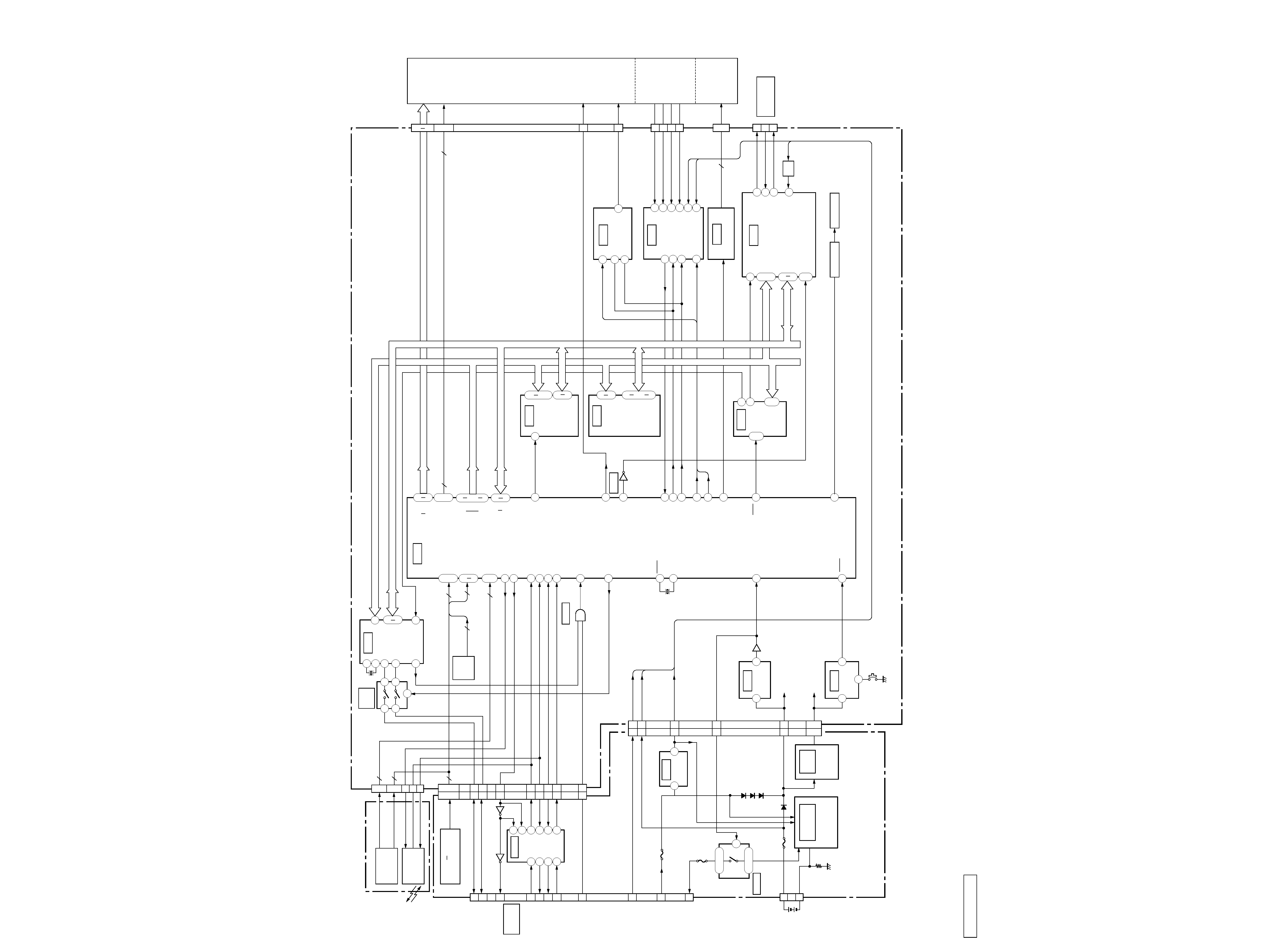
SECTION 2
BLOCK DIAGRAM
-- 5 --
-- 6 --
1
20
15
12
13
10
16
17
8
9
14
11
26
1
2
25
23
22
28
18
16
32
13
20
14
15
55
26
47
19
23
24
56
3
6
28
47
77
1
2
4
57
38
26
12
14
16
15
2
5
4
3
7
8
7
2
1
5
5
2
1
1
2
2
1
5
20
15
16
17
34
52
10
9
11
X101
32.768KHz
MP-23 BOARD
CNX-98 BOARD
FP-001 BOARD
1
5
3
4
6
7
8
CN402
2
2
6
JOG A, B
KB ROW1
KB COL2
SD IRDA
RXD
TXD
S1001
JOG
IC1001
IRDA
S901
S906
KEY MATRIX
1
2
3
4
6
5
7
IC104
IC651
IC981
IC701
IC702
IC703
IC952
IC951
IC954,955
D-
D+
DTR
RXD
TXD
RTS
CTS
RXD
TXD
RTS
CTS
HOT SYNC
CN902
CN902
CN401
CN401
18
17
19
20
8
9
7
6
9
8
15 11
6
7
4
5
10
22
21
20
25
16
Q652
Q651
KB ROW0-2
KB COL0-2
RS232C
I/F
CN901
CRADLE
10
17
18
12
9
11
CNT
DC +B
F951
UNREG OUT
DC IN
DETECT
LOW BAT
TH981
2,4,8,10
1,3,9
D962
D963
D964
BATTERY
BATT+
BATT-
CN951
16
F952
D953
BATTERY
CHARGE
CONTROL
DC/DC
CONV.
LOW BAT
DETECT
UNREG
3.3V
RESET
DETECT
S101
RESET
Q101
RESET
CSA1
EXTAL
XTAL
LOW BAT
SPK
RX SPI
TX SPI
CLK SPI
TO/TI
CS ADC
CS CCFL
KB ROW02
KB COL02
JOG A,B
SD IRDA
SD 232C
RXD
RXD
RTS
CTS
IRQ1
USB ON
IRQ USB
IRQ HOTSYNC
1
2
4
BATT+
DC IN C
CNT
37
6
7
36
34
30
82
1
9
46
43
42
41
39
83
100
1
5
75
59
X701
6MHz
USB
I/F
S153
POWER
SW
KB ROW2
KB COL0
2
3
3
2
A1
DOD7
CS USB
CPU
LDO
LD3
LFRM
LLP
LCLK
LDOLD3
3
A1
A21
D0
D15
A1A2
D0D15
CS FLASH
32Mbit
FLASH
64Mbit
EDO
DRAM
CHIP
SELECT
MEMORY STICK
I/F
TOUCH PAD
A/D
CONV.
EL DRIVE
CONTRAST
ADJ
LCD
MODULE
160 X 160
TOUCH
PAD
EL
BACK
LIGHT
X+
Y-
X-
Y+
8
6
4
2
1
2
2
CN301
CN302
CN801
12
13
DISF ON
VADJ
CNT
BATT+
EL1,2
BS
DIO
SCLK
DC IN C
SW
Q502
Q451,452
BUFFER
SP451
BUZZER
CLK
D0D15
A1A3
CS MS
CN501
MEMORY
STICK
2
4
8
RX SPI
TX SPI
CLK SPI
TO/TI
TX SPI
CLK SPI
3
D0D15
D0D15
A1A13
A1A17
LD0LD3
LFRM,LLP
LCLK
DISP ON
DISP ON
CLK
34
25
1
48
29
45
19
33
2
10
41
44
2
5
1
7
CS USB
CS MS
A20
38
37
36
40
10
13
28
CS ADC
8
5
11
10
9
IC601
IC602
IC106
IC103
IC101
IC201
IC202
IC102
IC105
IC501
IC301
IC304
23 3
719
16
10
15
11
14
12
IC303
PEG-S300,S300/HK
Confidential
SECTION 3
PRINTED WIRING BOARDS AND SCHEMATIC DIAGRAMS
-- 7 --
-- 8 --
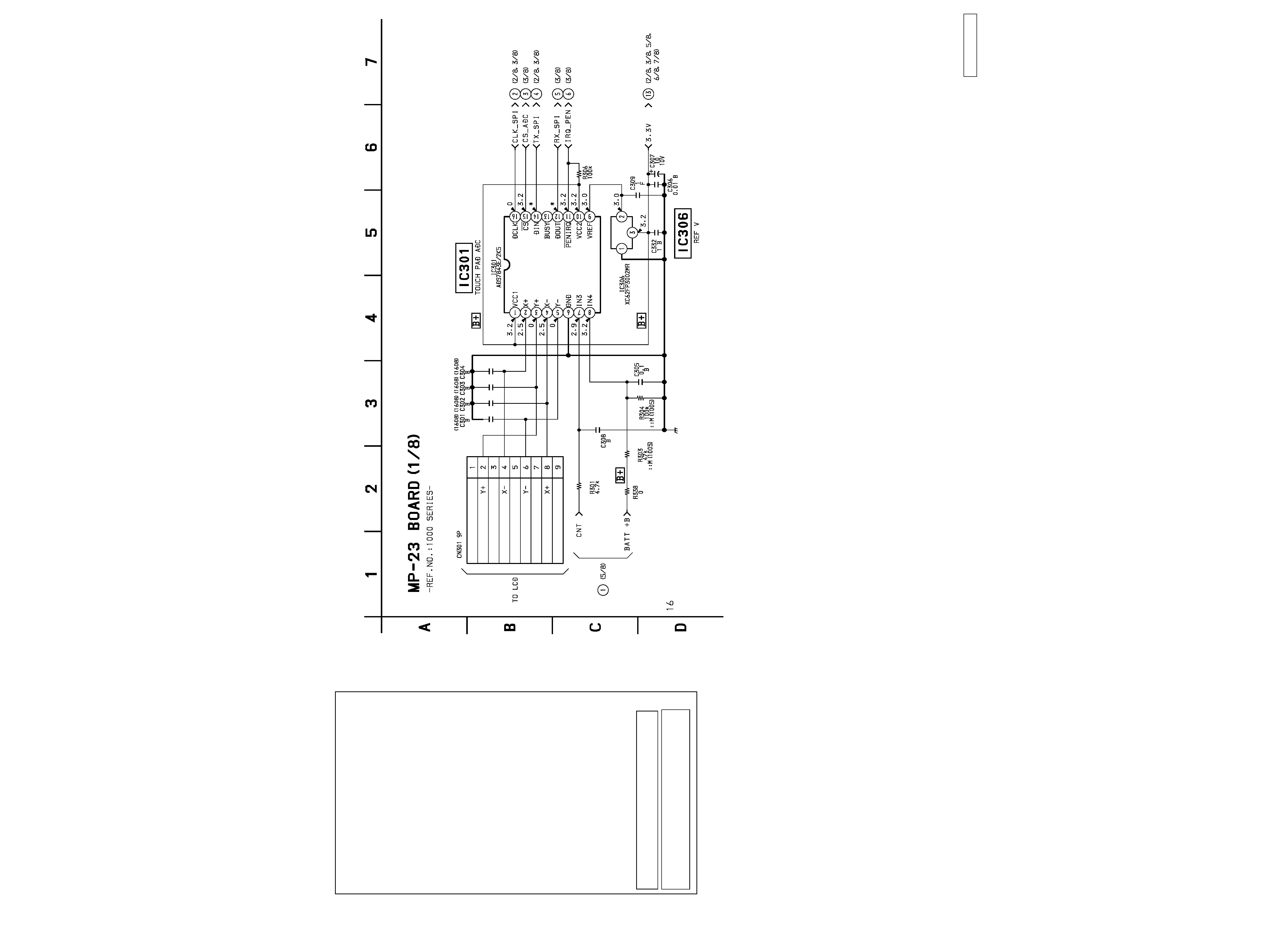
MP-23 (TOUCH PAD A/D CONVERTER) SCHEMATIC DIAGRAM
-- Ref. No. MP-23 board; 1,000 Series --
For Schematic Diagram
· Refer to page 23 for Printed Wiring Board.
(For printed wiring boards)
· b: Pattern from the side which enables seeing.
(The other layers' patterns are not indicated.)
· Through hole is omitted.
· There are few cases that the par t printed on diagram
isn't mounted in this model.
(For schematic diagrams)
· All capacitors are in
µF unless otherwise noted. pF : µµF.
50V or less are not indicated except for electrolytics and
tantalums.
· All resistors are in
and 1/4W or less unless otherwise specified.
· Chip resistors are 1/10W unless otherwise noted.
k
=1000, M=1000k.
· Caution when replacing chip parts.
New parts must be attached after removal of chip.
Be careful not to heat the minus side of tantalum capacitor, Be-
cause it is damaged by the heat.
· All variable and adjustable resistors have characteristic curve B,
unless otherwise noted.
· 2 : non flammable resistor
· C : panel designation
·
f
: internal component.
· U : B+ Line.
· V : B Line.
· Circled numbers refer to waveforms.
· Voltage variations may be noted due to normal production
tolerances.
· Voltages are taken with a VOM (Input impedance 10 M
).
THIS NOTE IS COMMON FOR PRINTED WIRING
BOARDS AND SCHEMATIC DIAGRAMS.
(In addition to this, the necessary note is
printed in each block.)
When indicating parts by reference number, pleas include
the board name.
Note: The components identified by mark 0 or dotted line
with mark 0 are critical for safety.
Replace only with part number specified.