Confidential
PCG-Z1A
SERVICE MANUAL
Notebook Computer
For American Area
US Model
Canadian Model
Illust : PCG-Z1A
9-876-076-02
Ver 2-2003D
Revision History
·Design and specifications are subject to
change without notice.
Lineup : PCG-Z1A

2
PCG-Z1A (AM)
Confidential
Information in this document is subject to change without notice.
Sony, VAIO and CLIE are trademarks or registered trademarks of
Sony. Microsoft, Windows, Windows Media, Outlook, Bookshelf
and other Microsoft products are trademarks or registered trademarks
of Microsoft Corporation in the United State and other countries.
The word Bluetooth and the Bluetooth logo are trademarks of
Bluetooth SIG, Inc. AMD, theAMD logo, other AMD product names
and combinations thereof are trademarks of Advanced Micro
Devices, Inc. Intel Inside logo, Pentium and Celeron are trademarks
or registered trademarks of Intel Corparation. Transmeta, the
Transmeta logo, Crusoe Processor, the Crusoe logo and combinations
thereof are trademarks of Transmeta Corporation in the USA and
other countries. Graffiti, Hotsync, PalmModem, and Palm OS are
registered trademarks, and the Hotsync logo and Palm are trademarks
of Palm, Inc. or its subsidiaries. (M) and Motrola are trademarks of
Motrola, Inc. Other Motrola pruducts and services with (R) mark
like Dragomball are the trademarks of Motrola, Inc.
All other name of systems, products and services in this manual are
trademarks or registered trademarks of their respective owners.
In this manual, the (TM) or (R) mark are not specified.
Caution Markings for Lithium/Ion Battery - The following or similar
texts shall be provided on battery pack of equipment or in both the
operating and the service instructions.
CAUTION: Danger of explosion if battery is incorrectly replaced.
Replace only with the same or equivalent type recommended by the
manufacturer. Discard used batteries according to the manufacturer's
instructions.
CAUTION: The battery pack used in this device may present a fire
or chemical burn hazard if mistreated. Do not disassemble, heat above
100
°C (212°F) or incinerate.
Dispose of used battery promptly.
Keep away from children.
CAUTION: Changing the back up battery.
·Overcharging, short circuiting, reverse charging, multilation or
incineration of the cells must be avoided to prevent one or more of
the following occurrence; release of toxic materials, release of
hydrogen and/or oxygen gas, rise in surface temperature.
· If a cell has leaked or vented, it should be replaced immediately
while avoiding to touch it without any protection.
Service and Inspection Precautions
1.
Obey precautionary markings and instructions
Labels and stamps on the cabinet, chassis, and components identify areas
requiring special precautions. Be sure to observe these precautions, as
well as all precautions listed in the operating manual and other associated
documents.
2.
Use designated parts only
The set's components possess important safety characteristics, such as
noncombustibility and the ability to tolerate large voltages. Be sure that
replacement parts possess the same safety characteristics as the originals.
Also remember that the
! mark, which appears in circuit diagrams and
parts lists, denotes components that have particularly important safety
functions; be extra sure to use only the designated components.
3.
Always follow the original design when mounting
parts and routing wires
The original layout includes various safety features, such as inclusion of
insulating materials (tubes and tape) and the mounting of parts above the
printer board. In addition, internal wiring has been routed and clamped so
as to keep it away from hot or high-voltage parts. When mounting parts
or routing wires, therefore, be sure to duplicate the original layout.
4.
Inspect after completing service
After servicing, inspect to make sure that all screws, components, and wiring
have been returned to their original condition. Also check the area around
the repair location to ensure that repair work has caused no damage, and
confirm safety.
5.
When replacing chip components...
Never reuse components. Also remember that the negative side of tantalum
capacitors is easily damaged by heat.
6.
When handling flexible print boards...
· The temperature of the soldering-iron tip should be about 270
°C.
· Do not apply the tip more than three times to the same pattern.
· Handle patterns with care; never apply force.
Caution: Remember that hard disk drives are easily damaged by
vibration. Always handle with care.
ATTETION AU COMPOSANT AYANT RAPPORT
À LA SÉCURITÉ!
LES COMPOSANTS IDENTIFÉS PAR UNE MARQUE !
!
!
!
! SUR LES
DIAGRAMMES SCHÉMATIQUES ET LA LISTE DES PIÈCES SONT
CRITIQUES POUR LA SÉCURITÉ DE FONCTIONNEMENT. NE
REMPLACER CES COMPOSANTS QUE PAR DES PIÈSES SONY
DONT LES NUMÉROS SONT DONNÉS DANS CE MANUEL OU
DANS LES SUPPÉMENTS PUBLIÉS PAR SONY.

3
PCG-Z1A (AM)
Confidential
History of the changes is shown as the
Revision History at the end of this data.
TABLE OF CONTENTS
Section
Title
Page
CHAPTER 1. BLOCK DIAGRAM ............................. 1-1
(to 1-2)
CHAPTER 2. FRAME HARNESS DIAGRAM ......... 2-1
(to 2-2)
CHAPTER 3. EXPRODED VIEWS AND
PARTS LIST ......................................... 3-1
3-1. Main Section .............................................................. 3-2
3-2. LCD Section .............................................................. 3-6
3-3. LCD Section (CTO Model) ....................................... 3-8
3-4. Accessories .............................................................. 3-10
(to 3-10)
PCG-Z1A (AM)
Confidential
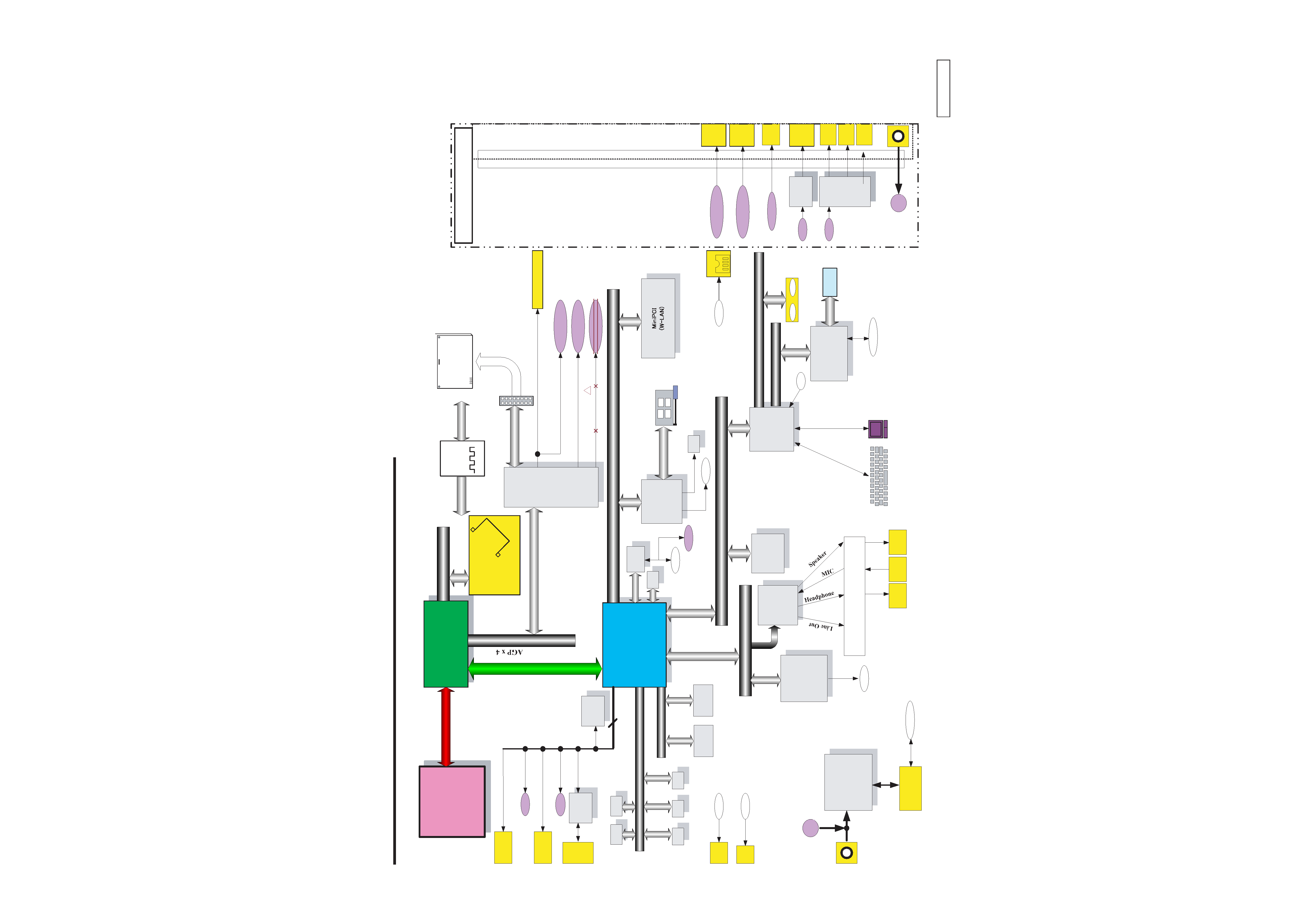
CHAPTER 1.
BLOCK DIAGRAM
(END)
11
12
[DEL]
CARDBUS
& i.LINK
RICOH
R5C551
Memory
CONTROLLER
HUB (MCH)
732 FCBGA
IO Control Hub
ICH4-m
421mBGA
Internal
HDD
PHONE
OUT
RJ11
MIC
IN
RJ45
Pentium-M
Processor
1MB L2
479pins
uFCBGA
PCI BUS(3.3V)
266MHz Memory Bus
(DDR)
CardBus/16bitCard
PC Card
Connector
1 Slot
H8S/2160
KBC/EC
SPIC
Graphics
M6-C16
(ATI)
LCD CONN
Cable
Ether
PHY
Internal KeyBoard
Membrane
VGA DSUB-15
LPC
i.LINK0
AC LINK
Speaker
L&R
I/O Expander
& SM BUS MUX
LID
Refer to Clock Generator
Block Diagram
SMBUS2
USB Left
CONN
TouchPad
EEPROM
For VID
EEPROM
For i.LINK
MDC
(Modem
Daughter
Card)
Module
CPU Local Bus
EEPROM
For Password
i.LINK
Dock-VGA DB-15
Dock-VGA DB-15
RJ-45
RJ45
VGA
DB-15
USB
CONN
USB
CONN
Port0-5
Primary
IDE(ATA100)
AMP, etc.
RJ-45
RJ-45
CLKGEN
ICS
950812YGD
Port Repricator
i.LINK0
Port-3
Port-0
Port-1
Port-2
Port-4
Port-5
RJ-45
RJ-11
RJ-11
Battery
Power
Circuit
DC Jack
On Board
Memory
256MB
or
+
512MB
SDRAM
SO-DIMM
SMBUS2
SMBUS2
SMBUS1
SMBUS0
DC Jack
DCin
DCin
BATTERY1
BATTERY1
FAN0
ATF0
Other
Control
FWH
8Mb
(Flash BIOS
ROM)
USB3
USB1
USB3
USB1
Audio
YMF753
(Yamaha)
SONY
EEPROM
For LAN
EEPROM
For ClockGEN
EEPROM
On DIMM1
For SPD
EEPROM
On DIMM2
For SPD
LCD
SXGA+(14)
XGA(14)
DVI
Dock-DVI
Dock-DVI
MS
CONN
Memory
Stick
Module
Bluetooth
Module
Optical
drive
Secondary
Dock-TV-out
USB Left
CONN
USB
CONN
PRT
DB-25
USB=>PRT
PL-2305
USB HUB
UPD720110
1
PCG-Z1A (AM)
Confidential
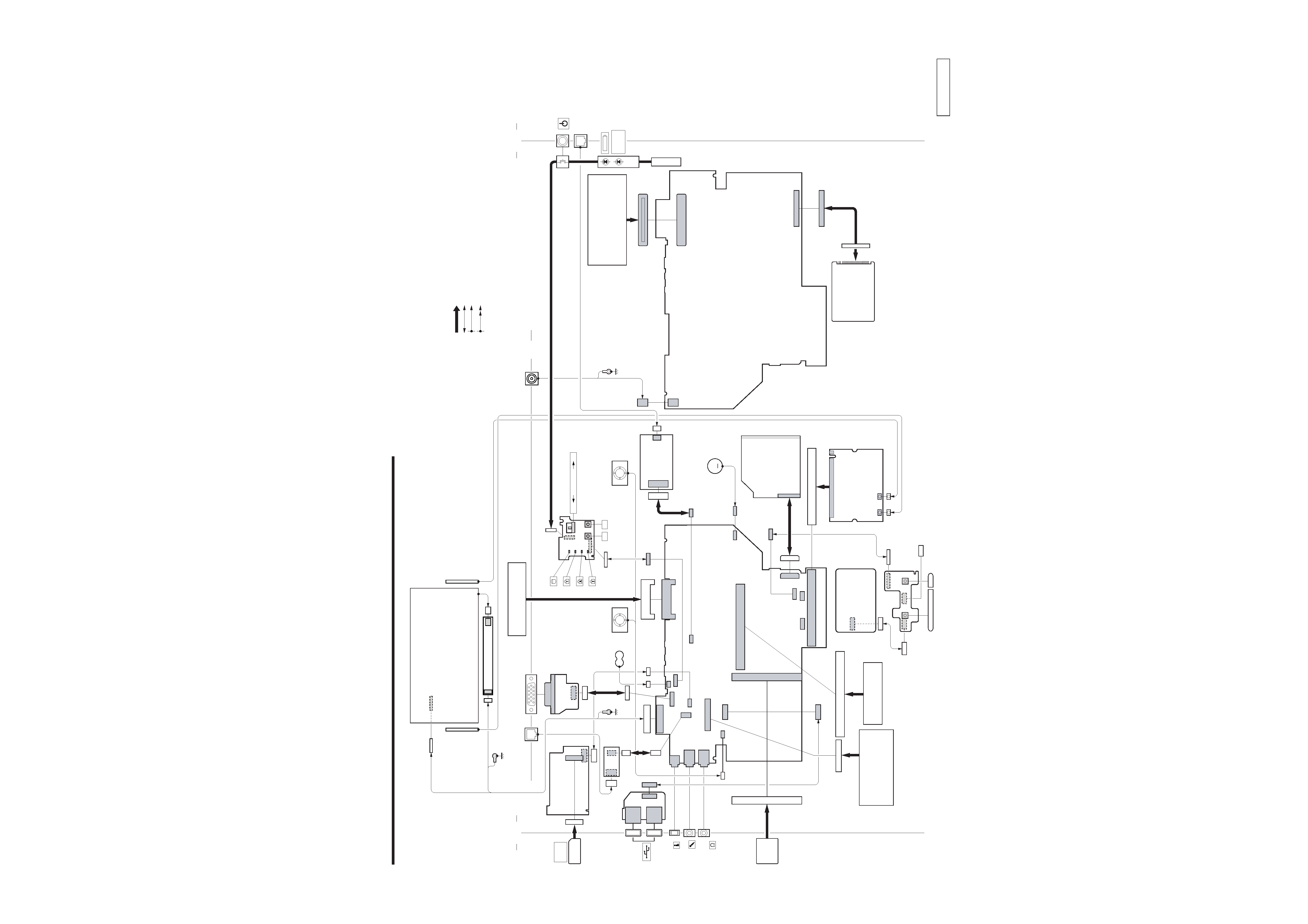
CHAPTER 2.
FRAME HARNESS DIAGRAM
(END)
21
22
Side R
POWER
DC IN 16V
Rear
PORT REPLICATOR
PCGA-PRZ1
1
2
100
99
MODULAR
JACK
Wireless
LAN
HDD
CN1202
150
MBX-71
BOARD
SIDE B
CN1601
1
3
123
J5
J6
CD-R/RW/
DVD-ROM
DRIVE
DC FAN
MOTOR
WIRELESS
LAN
CARD
2
4
124
CN5100
S5101
S5100
CN5102
CN5101
1
1
12
1
6
14
SWX-132
BOARD
SIDE B
TOUCH
PAD
CN801
CN4502
199
1
2
30
2
2
1
2
23
24
CN2601
10
1
MEMORY CARD
(EXPANSION MEMORY)
KEYBOARD
UNIT
CN4501
34
68
200
29
1
CN2821
J2150
J2250
CN1401
1
35
1
2
1
23
CN2270
14
PC
CARD
CN1394
CN5402
CN5401
CN2602
CN3902
1
1
4
1
4
4
3
9
10
1
2
2
1
CN2702
CN5500
FFC MBX-IFX248
FPC
(OPT)
FPC (HDD)
FFC
SWX132-TP
FFC
MBX-SWX132
CN5501
15
1
CN721
1
39
CN1501
CN5300
21
89
21
1
1
6
11
5
10
15
15
1
10
8
9
CN4051
8
MBX-71
BOARD
SIDE A
CNX-199
BOARD
SIDE A
IFX-249
BOARD
SIDE B
CN4602
MEMOR
Y
STICK
CONNECT
OR
LCD
HARNESS
FPC
(V
GA)
RJ-45
HARNESS
PC
CARD
CONNECT
OR
IFX-248
BOARD
SIDE A
CNX-200
BOARD
SIDE B
1
10
CN5301
1
9
BATTERY
SPEAKER
L ch
HEAD
PHONE
MIC
USB
MEMORY
STICK
i LINK
MAGIC
GATE
CN5400
1
10
BATTERY PACK
LCD
UNIT
INVERTER UNIT
WIRELESS
LAN ANT
(R)
WIRELESS
LAN ANT
(L)
NETWORK
MONITOR
Side L
1
15
16
2
CN2901
J1
J2
1
SWX-131
BOARD
SIDE A
S6002 S6003
D6003
D6000
D6001
D6002
CN6001
8
1
CN6000
FFC
MBX-SWX131
FPC (LED-W)
HARNESS (RJ11)
FPC
(MODEM)
CABLE
ASSY
16
1
MODEM
CARD
OFF
WIRELESS
ON
S6003
P1
P2
SPEAKER
R ch
CN1202
CN60
1
2
CN2001
CN3901
1
10
9
2
CN2801
14
13
2
1
M
1
2
1
2
49
50
119
20
From board to connector (direct connection)
Harness (connector at both end)
Harness (soldered at one end)
Connectors soldered on board and appearing on the panel
HARNESS
(WITH
DC
JACK
2P)
CN2701