1
MICROFILM
MZ-E60
SERVICE MANUAL
PORTABLE MINIDISC PLAYER
SPECIFICATIONS
US Model
Canadian Model
AEP Model
E Model
System
Audio playing system
MiniDisc digital audio system
Laser diode properties
Material: GaAlAs
Wavelength:
= 790 nm
Emission duration: continuous
Laser output: less than 44.6
µW
(This output is the value measured at a distance
of 200 mm from the objective lens surface on the
optical pick-up block with 7 mm aperture.)
Revolutions
800 rpm to 1,800 rpm
Error correction
Advanced Cross Interleave Reed Solomon
Code (ACIRC)
Sampling frequency
44.1 kHz
Coding
Adaptive TRansform Acoustic Coding (ATRAC)
Modulation system
EFM (Eight to Fourteen Modulation)
Number of channels
2 stereo channels
1 monaural channel
Frequency response
20 to 20,000 Hz ± 3 dB
Wow and Flutter
Below measurable limit
Outputs
Headphones: stereo mini-jack,
maximum output level 5 mW + 5 mW, load
impedance 16 ohms
General
Power requirements
One LR6 (size AA) battery (not supplied)
Battery operation time
You can check the battery condition with the
battery indication which is displayed while using
the player.
t Battery power decreasing
v
r Weak battery
v
e The battery has gone out. "LOW BATT"
flashes in the display on the remote control,
and the power goes off.
Battery Life
Approximately 12 hours of playback can be
expected with one LR6 (size AA) alkaline battery
(not supplied).
Note
The battery life may shorter depending on
operating conditions and temperature of the
location.
Continued on next page
US and foreign patents licensed from Dolby
Laboratories Licensing Corporation.
Model Name Using Similar Mechanism
MZ-E90
MD Mechanism Type
MT-MZE60-169
Optical Pick-up Mechanism Type
LCX-2E
(Photo: Silver)
Ver 1.1 2000. 06
With SUPPLEMENT-1
(9-927-633-81)
2
SAFETY-RELATED COMPONENT WARNING!!
COMPONENTS IDENTIFIED BY MARK
0 OR DOTTED LINE WITH
MARK
0 ON THE SCHEMATIC DIAGRAMS AND IN THE PARTS
LIST ARE CRITICAL TO SAFE OPERATION.
REPLACE THESE COMPONENTS WITH SONY PARTS WHOSE
PART NUMBERS APPEAR AS SHOWN IN THIS MANUAL OR IN
SUPPLEMENTS PUBLISHED BY SONY.
Flexible Circuit Board Repairing
· Keep the temperature of the soldering iron around 270°C
during repairing.
· Do not touch the soldering iron on the same conductor of the
circuit board (within 3 times).
· Be careful not to apply force on the conductor when soldering
or unsoldering.
Notes on chip component replacement
· Never reuse a disconnected chip component.
· Notice that the minus side of a tantalum capacitor may be
damaged by heat.
Precautions for Laser Diode Emission Check
When checking the emission of the laser diode during adjust-
ments, never view directly downwards as this may lead to
blindness.
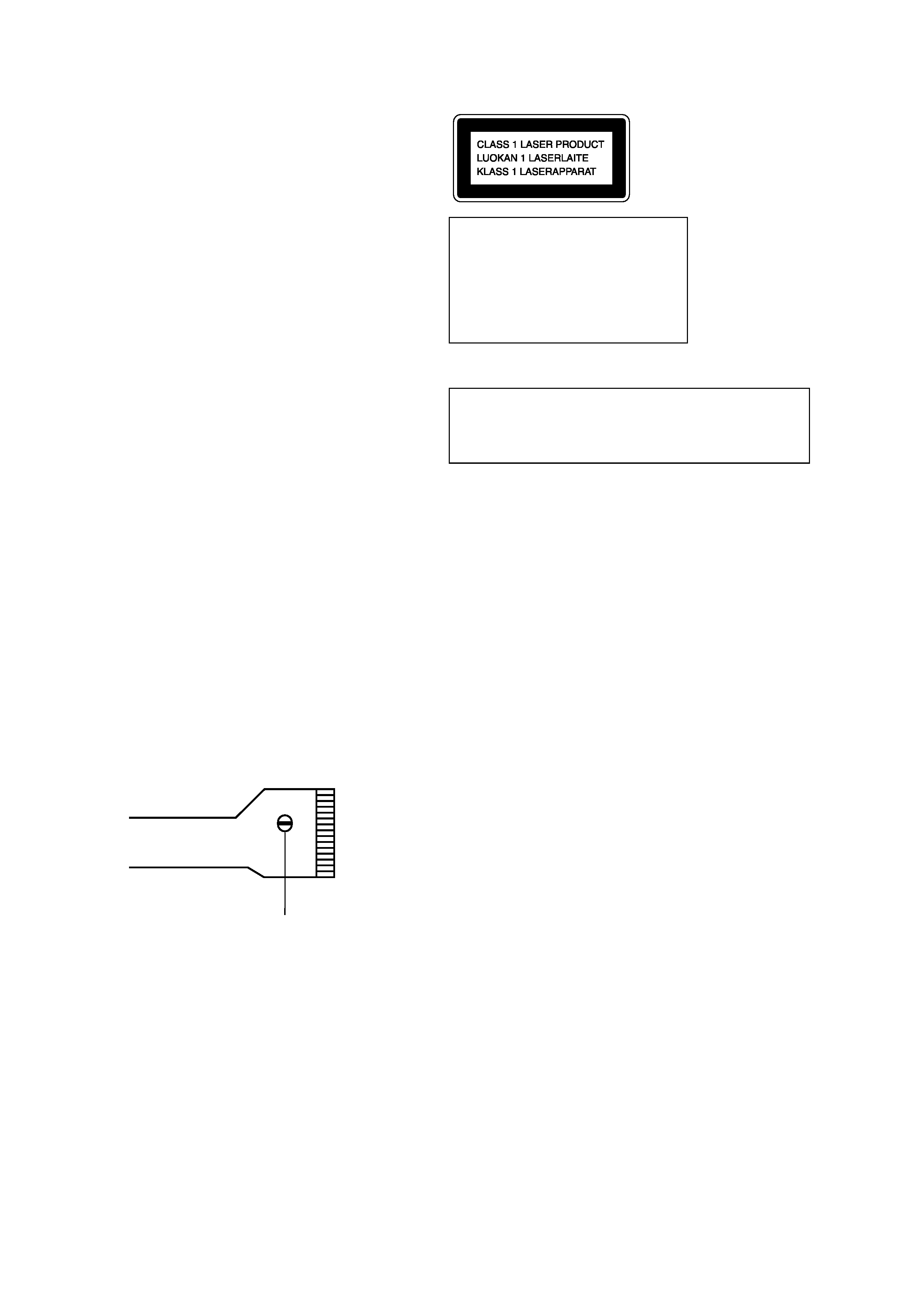
Precautions for Using Optical Pick-up (LCX-2E)
As the laser diode inside the optical pick-up damages by static
electricity easily, solder the laser tap of the Optical pick-up
flexible board when handling. Also take the necessary measures
to prevent damages by static electricity. Handle the Optical pick-
up flexible board with care as it breaks easily.
Laser tap
Optical Pick-up flexible board
CAUTION
Use of controls or adjustments or performance of procedures
other than those specified herein may result in hazardous
radiation exposure.
IN NO EVENT SHALL SELLER BE
LIABLE FOR ANY DIRECT,
INCIDENTAL OR CONSEQUENTIAL
DAMAGES OF ANY NATURE, OR
LOSSES OR EXPENSES RESULTING
FROM ANY DEFECTIVE PRODUCT
OR THE USE OF ANY PRODUCT.
"MD WALKMAN" is a trademark of Sony
Corporation.
This MiniDisc player is classi-
fied as a CLASS 1 LASER
product.
The CLASS 1 LASER
PRODUCT label is located on
the bottom exterior.
Dimensions
Approx. 81
× 25 × 74 mm (w/h/d)
(3 1/4
× 1 × 3 in.) not including projecting
parts and controls
Mass
Approx. 95 g (3.4 oz.) the player only
Approx. 136 g (4.8 oz.) incl. a premastered MD
and a LR6 (size AA) alkaline battery
Supplied accessories
Headphones with a remote control (1)
Carrying pouch (1)
Design and specifications are subject to change
without notice.
ATTENTION AU COMPOSANT AYANT RAPPORT
À LA SÉCURITÉ!!
LES COMPOSANTS IDENTIFIÉS PAR UNE MARQUE
0 SUR LES
DIAGRAMMES SCHÉMATIQUES ET LA LISTE DES PIÈCES
SONT CRITIQUES POUR LA SÉCURITÉ DE FONCTIONNEMENT.
NE REMPLACER CES COMPOSANTS QUE PAR DES PIÈCES
SONY DONT LES NUMÉROS SONT DONNÉS DANS CE MANUEL
OU DANS LES SUPPLÉMENTS PUBLIÉS PAR SONY.

3
1. SERVICING NOTE ......................................................... 4
2. GENERAL ......................................................................... 5
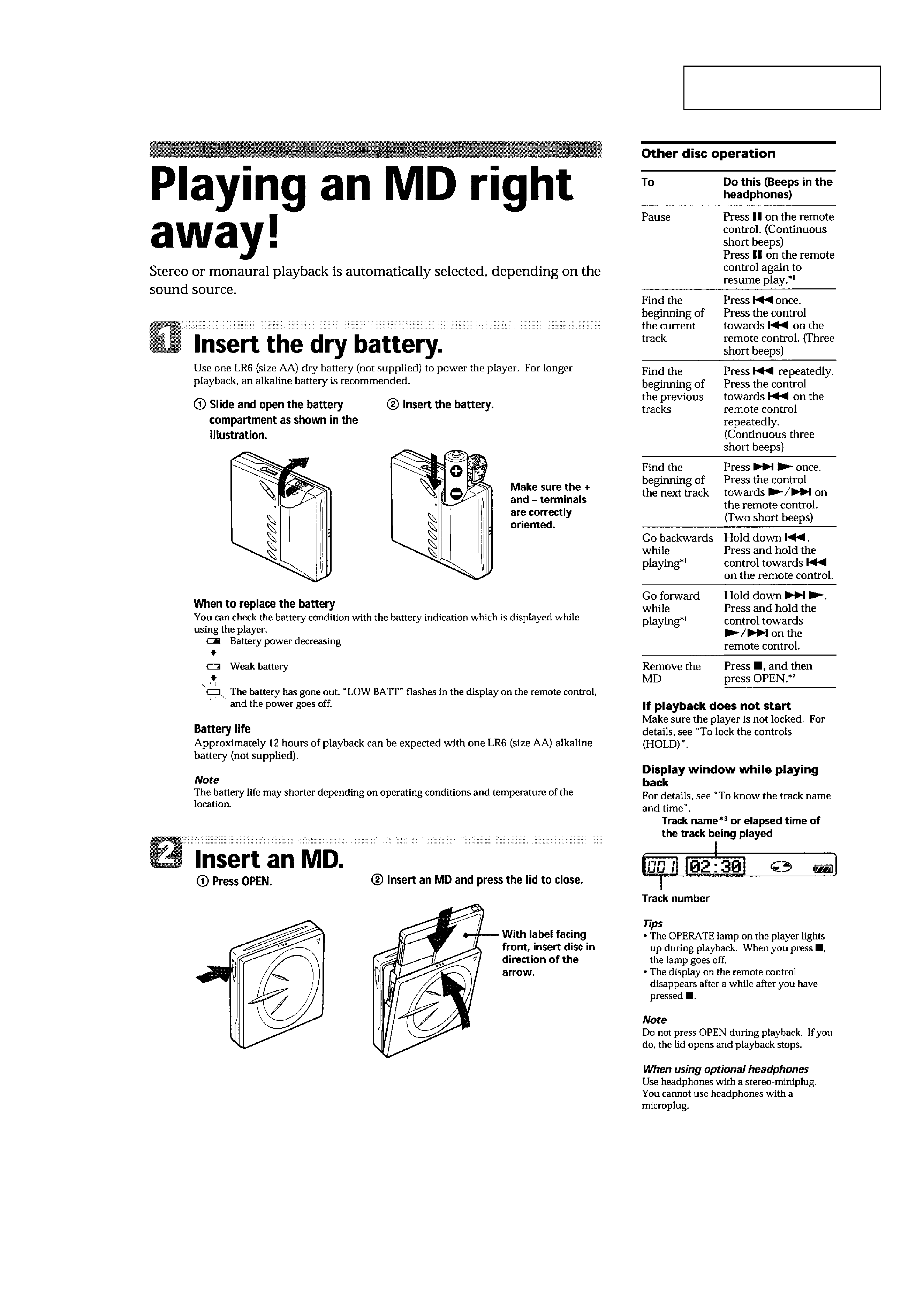
Playing an MD right away! ................................................... 5
3. DISASSEMBLY ............................................................... 7
3-1. Panel Assy, Upper ................................................................. 7
3-2. Holder Assy ........................................................................... 7
3-3. Mechanism Deck .................................................................. 8
3-4. Main Board ........................................................................... 8
3-5. Service Assy, OP ................................................................... 9
4. TEST MODE ................................................................... 10
4-1. General ................................................................................ 10
4-2. Setting the Test Mode ......................................................... 10
4-2-1. How to Set the Test Mode ........................................... 10
4-2-2. Operations when the Test Mode is Set ........................ 10
4-2-3. How to Release the Test Mode .................................... 10
4-3. Test Mode Structure ............................................................ 10
4-4. Manual Mode ...................................................................... 11
4-4-1. Outline of the Function ............................................... 11
4-4-2. How to Set the Manual Mode ...................................... 11
4-5. Overall Adjustment Mode ................................................... 11
4-5-1. Outline of the Function ............................................... 11
5. ELECTRICAL ADJUSTMENTS .............................. 12
5-1. General ................................................................................ 12
5-2. Notes for Adjustment .......................................................... 12
5-2-1. Jigs ............................................................................... 12
5-2-2. Adjustment Sequence .................................................. 12
5-2-3. Power ........................................................................... 12
5-3. Reset NV ............................................................................. 12
5-3-1. How to Reset NV ........................................................ 12
5-4. Overall Adjustment Mode ................................................... 12
5-4-1. Overall Adjustment Mode Structure ............................ 12
5-4-2. Overall CD and MO Adjustment Method ................... 12
5-4-3. Overall CD and MO Adjustment Items ....................... 13
TABLE OF CONTENTS
6. DIAGRAMS ..................................................................... 14
6-1. IC Pin Description .............................................................. 14
6-1-1. IC801 RU6915MF-0006 (System Control) ................. 14
6-2. Block Diagrams .................................................................. 17
6-2-1. MD Block Diagram ..................................................... 17
6-2-2. Servo, System Control Block Diagram ....................... 19
6-3. Printed Wiring Boards and Schematic Diagrams ................ 21
6-3-1. Printed Wiring Board Main Board ........................ 21
6-3-2. Schematic Diagram Main Board (1/4) .................. 25
6-3-3. Schematic Diagram Main Board (2/4) .................. 27
6-3-4. Schematic Diagram Main Board (3/4) .................. 29
6-3-5. Schematic Diagram Main Board (4/4) .................. 31
6-4. IC Block Diagrams ............................................................. 33
7. EXPLODED VIEWS ..................................................... 37
7-1. Main Unit Section ............................................................... 37
7-2. Mechanism Deck Section ................................................... 38
8. ELECTRICAL PARTS LIST ...................................... 39
4
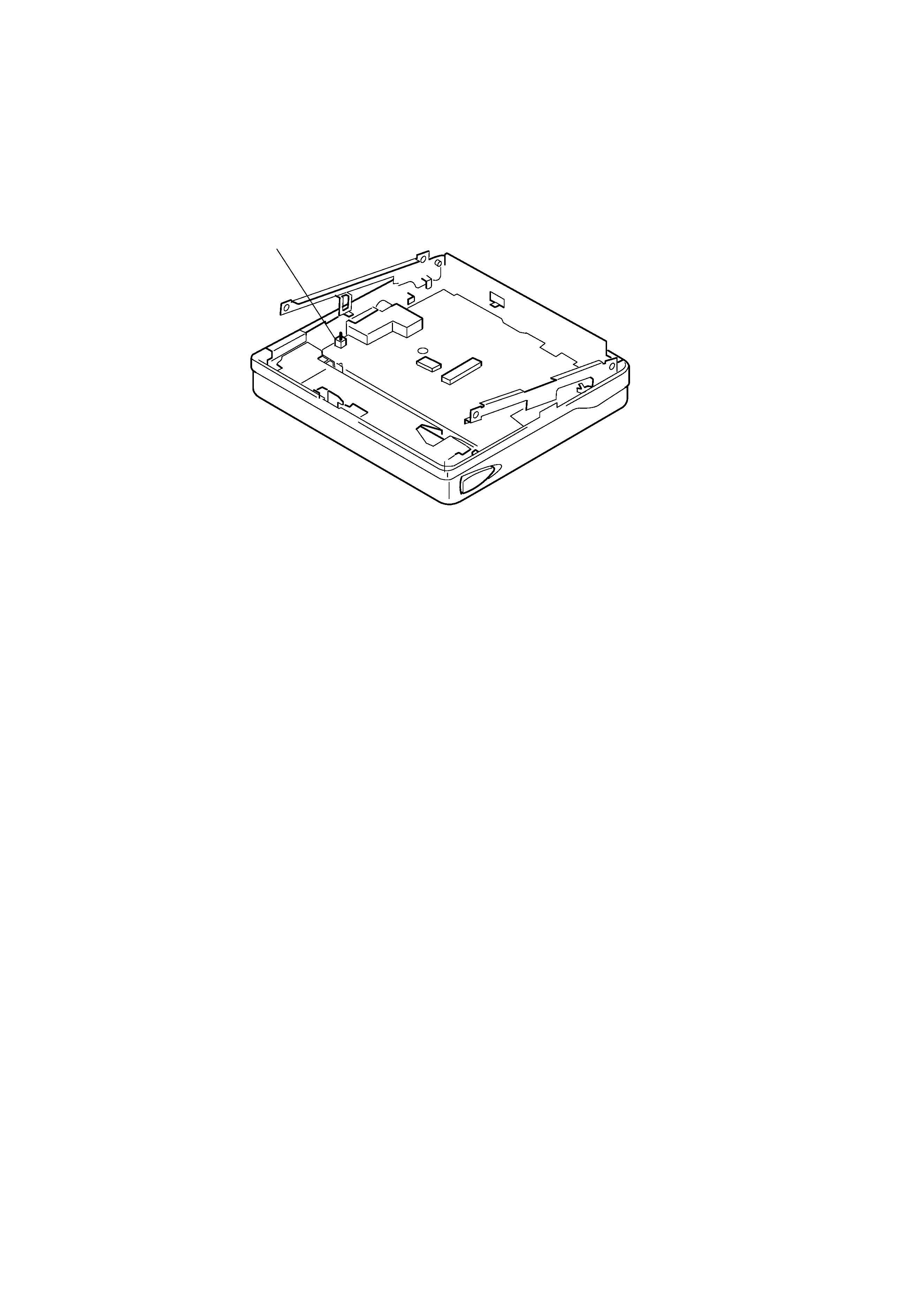
1) When repairing this device with the power on, if you remove
the main board or open the upper panel assy, this device stops
working.
In this case, you can work without the device stopping by
fastening the hook of the OPEN/CLOSE switch (MAIN board
S809) with tape.
2) This set is designed to perform automatic adjustment for each
adjustment and write its value to EEPROM. Therefore, when
EEPROM (MAIN board IC802) has been replaced in service,
be sure to perform automatic adjustment and write resultant
values to the new EEPROM.
Refer to section 4 Test Mode (page 10) for details.
SECTION 1
SERVICING NOTE
MAIN board S809
5
SECTION 2
GENERAL
This section is extracted from
instruction manual.