1
SERVICE MANUAL
AUDIO MIXER
US Model
AEP Model
UK Model
E Model
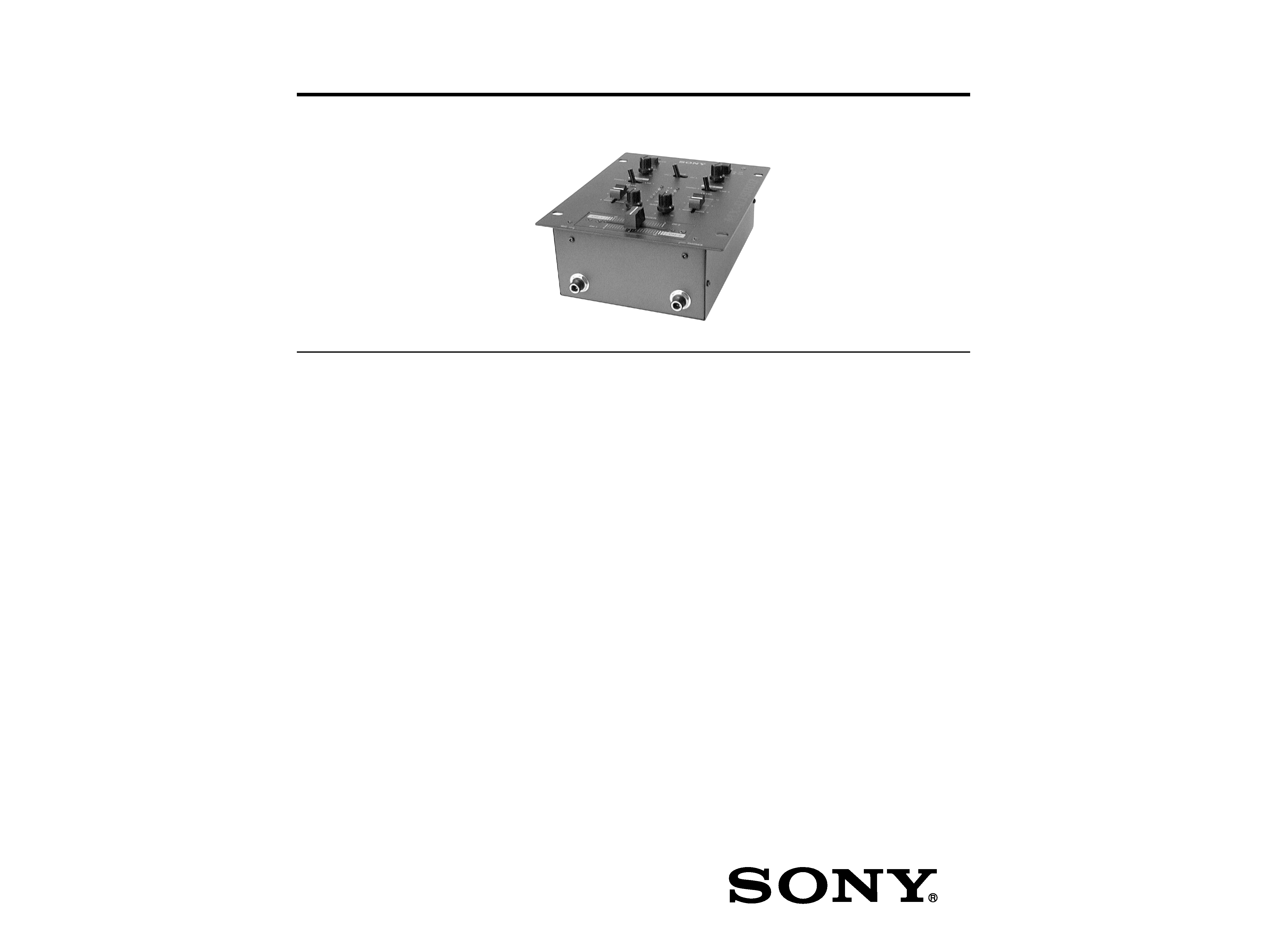
MX-DJ9000
SPECIFICATIONS
This set is the audio mixer in PMPK-DJ9000.
General
Power requirements
U.S.A. and Mexico: 120 V AC, 60 Hz
European countries: 220 - 230 V AC,
50/60 Hz
Other countries: 110 - 120 V/
220 - 240 V AC, 50/60 Hz
Power consumption
10 W
Inputs
2 PHONO, 2 LINE, 1 MIC
Microphone
1.5 mV
Phono
3 mV
Line
150 mV
Output power
7 V (peak-to-peak)
Outputs
1 LINE OUT, 1 REC OUT via RCA
Frequency range
20 - 20,000 Hz,
±3 dB
Distortion
Less than 0.08 %
S/N ratio
70 dB (1 kHz)
Talkover attenuation
16 dB
Headphones impeadance
16
Dimensions
Approx. 200
× 80 × 166 mm (7 7/ 8 ×
3
× 6
in) (w/h/d)
1/4
5/8
Mass
1.6 kg (3 lb 8 oz)
Supplied Accessory
AC power adaptor cord (1)
Audio cord (without ground wire) (2)
Design and specifications are subject to change without
notice.

2
SAFETY-RELATED COMPONENT WARNING!!
COMPONENTS IDENTIFIED BY MARK 0 OR DOTTED LINE WITH
MARK 0 ON THE SCHEMATIC DIAGRAMS AND IN THE PARTS
LIST ARE CRITICAL TO SAFE OPERATION. REPLACE THESE
COMPONENTS WITH SONY PARTS WHOSE PART NUMBERS AP-
PEAR AS SHOWN IN THIS MANUAL OR IN SUPPLEMENTS PUB-
LISHED BY SONY.
TABLE OF CONTENTS
1. GENERAL
..................................................................... 3
2. DIAGRAMS
2-1.
Circuit boards Location ...................................................... 3
2-2.
Schematic Diagram ............................................................ 4
2-3.
Printed Wiring Board Main Section ............................. 5
2-4.
Printed Wiring Board I/O Section ................................ 6
3. EXPLODED VIEW
3-1.
Chassis Section ................................................................... 8
4. ELECTRICAL PARTS LIST .................................... 10
33
SECTION 2
DIAGRAMS
Note on Printed Wiring Board:
· X : parts extracted from the component side.
· Y : parts extracted from the conductor side.
· b : Pattern from the side which enables seeing.
Note on Schematic Diagram:
· All capacitors are in µF unless otherwise noted. pF: µµF
50 WV or less are not indicated except for electrolytics
and tantalums.
· All resistors are in
and 1/4 W or less unless otherwise
specified.
· C : panel designation.
· U : B+ Line.
· V : B Line.
· Voltages are dc with respect to ground under no-signal
conditions.
no mark : Power on
· Voltages are taken with a VOM (Input impedance 10 M
).
Voltage variations may be noted due to normal produc-
tion tolerances.
· Signal path.
F
: AUDIO
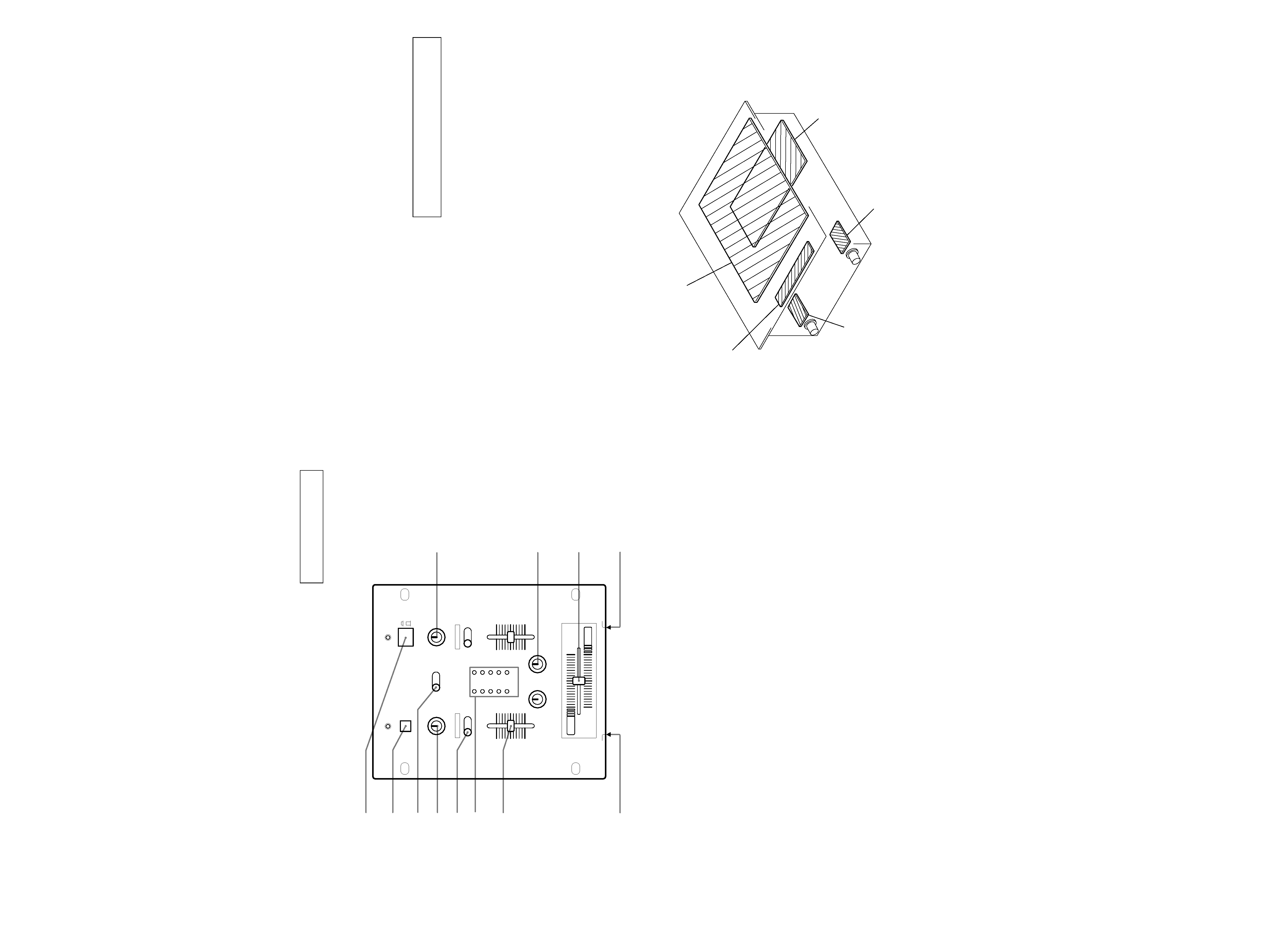
2-1. CIRCUIT BOARDS LOCATION
Note: The components identified by mark 0 or dotted line
with mark 0 are critical for safety.
Replace only with part number specified.
NOTE FOR PRINTED WIRING BOARD AND SCHEMATIC DIAGRAM
SECTION 1
GENERAL
MIC board
PHONE board
CROSSFADER unit
MAIN board
I/O board
1 POWER switch
2 TALK OVER button
Press this button to use the microphone.
3 CUE select switch
This switch selects CH-1 or CH-2 for headphone
listening.
4 MIC LEVEL control
Adjusts the microphone level.
5 PHONO/LINE switch
Selects the signal to be input to the respective
channel.
6 Channel level display
Shows the left and right levels of the output.
7 Channel level knob
Adjusts the level of each channel.
8 MIC jack
You can connect microphones with mono plug.
9 CUE LEVEL control
Adjusts the headphone volume without affecting
the output signal.
q; GAIN control
Use these controls to adjust the balance between
CH-1 and CH-2.
qa CROSSFADER knob
Mixes the signal of one channel with that of the
other.
qs PHONES jack
Use this jack to connect headphones. Accepts
headphone with an impedance of 16 ohms or
more, but 16 ohms is recommended. Select CH-1
or CH-2 with the CUE select switch.
1
9
0
qa
qs
2
3
4
5
6
7
8
MIC LEVEL
LEVEL
GAIN
CROSSFADER
TALK OVER
CUE
010
CH-1
0
10
5
0
CH-2
0
CH-1
MIC
PHONES
510
10
5
0
10
5
0
+3
0
-3
-8
-13
10
CH-2
010
CH-1
CH-1
CH-2
PHONO 1
LINE 1
CUE LEVEL
LEVEL
POWER
010
10
5
0
10
5
0
CH-2
PHONO 2
LINE 2
CH-1
CH-2
dB
LR
ON
OFF
This section is extracted from
instruction manual.
44
MX-DJ9000
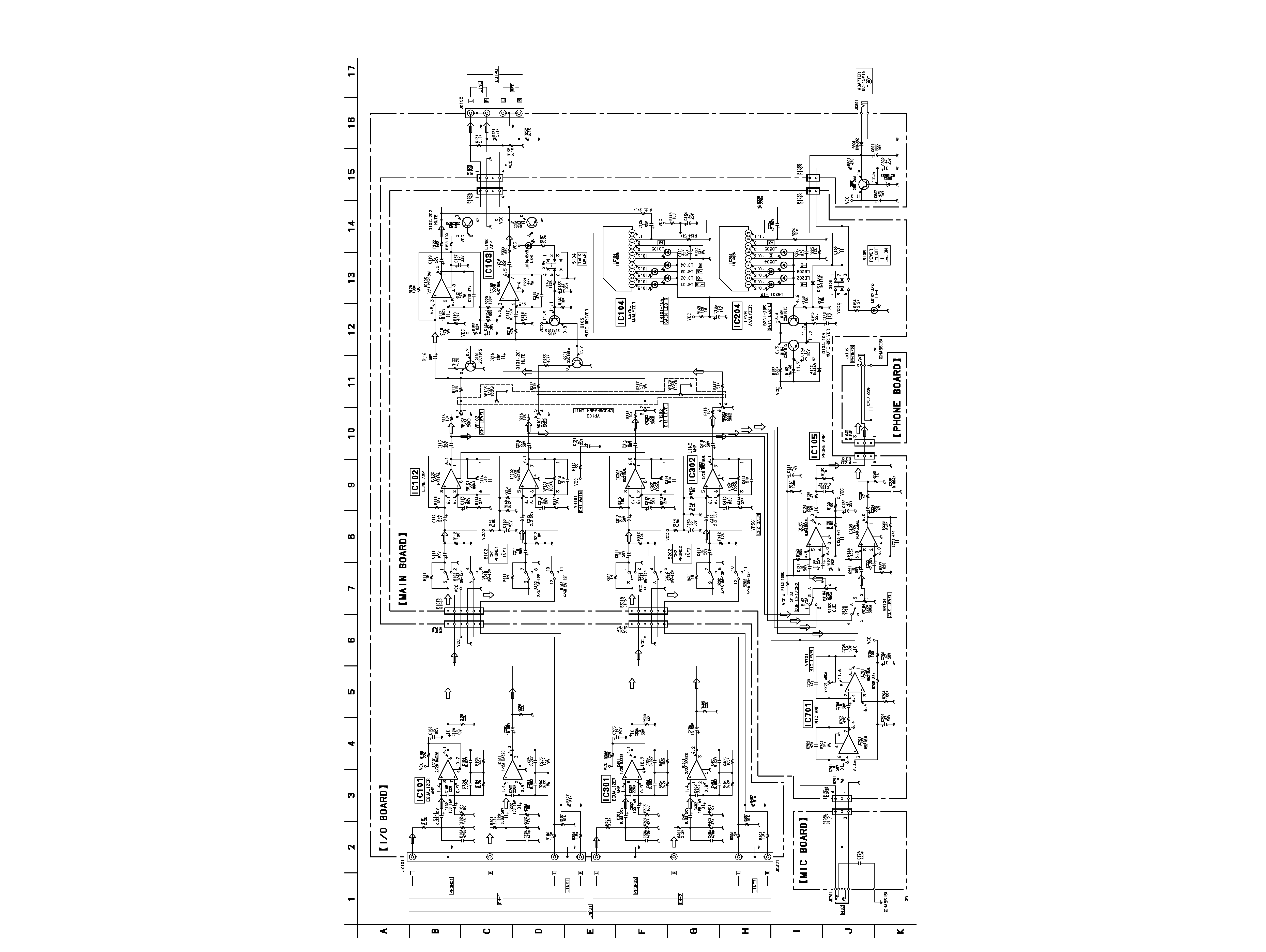
2-2. SCHEMATIC DIAGRAM · See Page 5 and 6 for Printed Wiring Boards.
55
MX-DJ9000
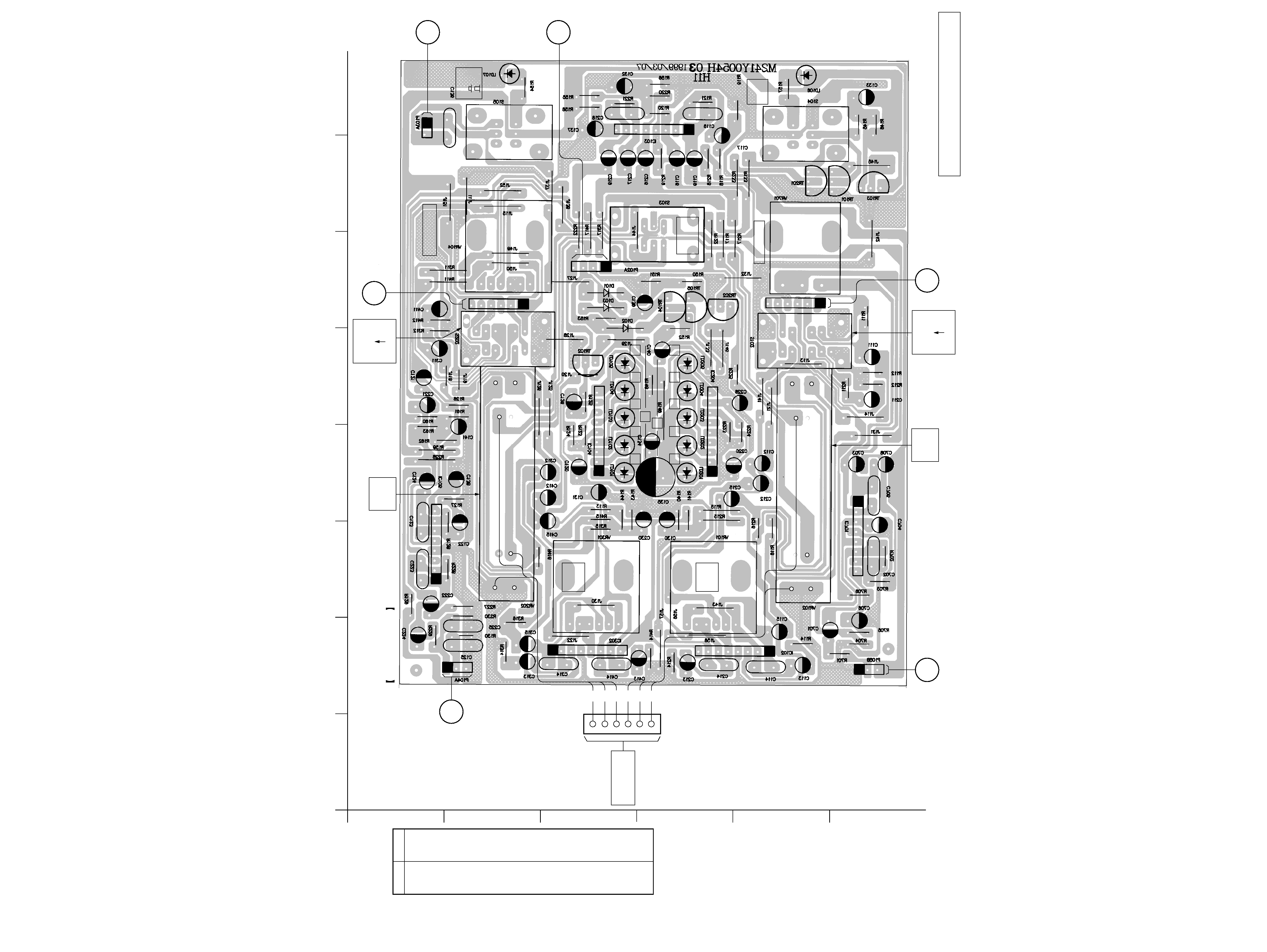
2-3. PRINTED WIRING BOARD MAIN SECTION · See Page 3 for Circuit boards Location. · See Page 4 for Schematic Diagram.
There are a few cases that the part isn't mounted in
model is printed on diagram.
D101
C-6
D102
C-6
D103
C-6
LD101
C-4
LD102
C-4
LD103
C-5
LD104
C-5
LD105
C-5
LD106
E-8
LD107
B-8
LD201
D-4
LD202
D-4
LD203
D-5
LD204
D-5
LD205
D-5
IC102
E-2
IC103
D-8
IC104
C-4
IC105
A-3
IC204
D-4
IC302
C-2
IC701
F-4
Q101
E-7
Q102
C-5
Q103
F-7
Q104
D-6
Q105
D-6
Q201
E-7
Q202
D-6
· Semiconductor
Location
Ref. No.
Location
1
1
12
3
45
6
3
2
4
4
6
5
6
5
3
2
-13
1
1
4
1
3
2
11
12
10
7
9
8
6
5
23
4
E
E
E
E
56
TALK
OVER
POWER
ON
OFF
MIC LEVEL
CUE
CH1/CH2
CUE LEVEL
P301B
P101B
D
E
B
A
F
C
CH2
LINE2
PHONO2
CH1
LINE1
PHONO1
CH2
LEVEL
CH2
GAIN
<1>
<2>
<5>
CH1
LEVEL
1
4
2
5
1
3
2
7
9
8
10
12
11
4
6
5
6
3
<5>
<2>
<1>
CH1
GAIN
CROSSFADER
UNIT
-8
-3
0
+3
-13
-8
-3
R
L
0
+3
MAIN BOARD
(Page 7)
(Page 7)
(Page 6)
(Page 6)
(Page 6)
(Page 6)
09
8
1
2
34
56
7
A
B
C
D
E
F