SERVICE MANUAL
Sony Corporation
Audio Entertainment Group
MINI HI-FI COMPONENT SYSTEM
2000D001623-1D
Printed in Japan ©2000. 4
Published by HA Quality Assurance Dept.
9-929-217-11
E Model
COMPONENT MODEL NAME
· MHC-VX88 is composed of following models.
As for the service manual, it is issued for each component model,
then, please refer to them.
SPEAKER SYSTEM
SS-RS158V
PARTS LIST
Part No.
Description
ACCESSORIES & PACKING MATERIALS
********************************
1-418-762-11 COMMANDER, STANDARD (RM-SV100) (EXCEPT E)
1-418-762-21 COMMANDER, STANDARD (RM-SV100B) (E)
1-501-374-11 ANTENNA, LOOP (AM)
1-501-659-11 ANTENNA (FM)
1-751-619-11 CORD, CONNECTION (VIDEO)
1-775-512-21 CORD, SPEAKER CONNECTION (FOR SS-VX88/VX88B)
1-790-115-11 CORD, SPEAKER (FOR SS-RS158V/RS158VB)
1-792-517-11 CORD (WITH CONNECTOR) (SYSTEM CONTROL)
4-210-254-01 CUSHION (FOOT) (FOR SS-VX88/VX88B)
4-226-944-11 MANUAL, INSTRUCTION (ENGLISH)
4-226-944-21 MANUAL, INSTRUCTION (FRENCH) (E, EA, MY, SP)
4-226-944-31 MANUAL, INSTRUCTION (SPANISH) ( E, MY, SP)
4-226-944-41 MANUAL, INSTRUCTION (CHINESE) (E, MY, SP)
4-226-944-51 MANUAL, I NSTRUCTION (ARABIC) (E, EA)
4-226-944-71 MANUAL, I NSTRUCTION (INDONESAN) (IA)
4-983-536-01 COVER, BATTERY (FOR RM-SV100B) (E)
4-983-536-01 COVER, BATTERY (FOR RM-SV100) (EXCEPT E)
MHC-VX88
TA-DX8
SS-VX88RS
HCD-VX88
VIDEO CD/CD PLAYER , DECK
AND RECEIVER SYSTEM
SS-VX88RSB
SS-RS158VB
SS-VX88
SS-VX88B
(Silver Model)
(Black Model)
(Color)
FRONT
SATELLITE
INTEGRATED STEREO
AMPLIFIER
· Abbreviation
EA
: Saudi Arabia
IA
: Indonesia
MY : Malaysia
SP
: Singapore
SS-DX8RS is composed SS-VX88 and SS-RS158V.
SS-DX8RSB is composed SS-VX88B and SS-RS158VB.
1
Amplifier section
The following measured at AC 120, 220, 240V
50/60 Hz
DIN power output (rated) 160 + 160 watts
(6 ohms at 1 kHz, DIN)
Continuous RMS power output (reference)
200 + 200 watts
(6 ohms at 1 kHz,
10% THD)
Inputs
MD/VIDEO (AUDIO) IN: voltage 450 mV/250 mV,
(phono jacks)
impedance 47 kilohms
MIC:
sensitivity 1 mV,
(phone jack)
impedance 10 kilohms
Outputs
VIDEO OUT:
max. output level 1 Vp-p,
(Phono jack)
unbalanced, Sync
negative, load impedance
75 ohms
S-VIDEO OUT:
Y: 1 Vp-p, unbalanced
(4 pin/mini-DIN jack)
Sync negative
C: 0.286 Vp-p
load impedence 75 ohms
PHONES:
accepts headphones of 8
(stereo mini jack)
ohms or more
FRONT SPEAKER:
accepts impedance of 6 to
16 ohms
SATELLITE SPEAKER:
accepts impedance of 6 to
16 ohms
VIDEO CD/CD player section
System
Compact disc and digital
audio system
Laser
Semiconductor laser
(
=780nm)
Emission duration:
continuous
Laser output
Max. 44.6
µW*
*This output is the value
measured at a distance of
200 mm from the
objective lens surface on
the Optical Pick-up Block
with 7 mm aperture.
Frequency response
2 Hz 20 kHz (
±0.5 dB)
Wavelength
780 790 nm
Signal-to-noise ratio
More than 90 dB
Dynamic range
More than 90 dB
Video color system format
NTSC, PAL
CD OPTICAL DIGITAL OUT
(Square optical connector jack, rear panel)
Wavelength
660 nm
Output Level
18 dBm
Tape player section
Recording system
4-track 2-channel stereo
Frequency response
40 13,000 Hz (
±3 dB),
(DOLBY NR OFF)
using Sony TYPE I
cassette
40 14,000 Hz (
±3 dB),
using Sony TYPE II
cassette
Tuner section
FM stereo, FM/AM superheterodyne tuner
FM tuner section
Tuning range
87.5 108.0 MHz
Antenna
FM lead antenna
Antenna terminals
75 ohm unbalanced
Intermediate frequency
10.7 MHz
AM tuner section
Tuning range
Middle Eastern models:
531 1,602 kHz
(with the interval set at 9
kHz)
Other models:
531 1,602 kHz
(with the interval set at 9
kHz)
530 1,710 kHz
(with the interval set at 10
kHz)
Antenna
AM loop antenna
Antenna terminals
External antenna terminal
Intermediate frequency
450 kHz
HCD-VX88
SERVICE MANUAL
HCD-VX88 is the tuner, tape player, VIDEO CD/
CD player and amplifier section in MHC-VX88.
SPECIFICATIONS
COMPACT DISC DECK RECEIVER
E Model
This stereo system is equipped with the Dolby B-
type noise reduction system*.
* Manufactured under license from Dolby
Laboratories Licensing Corporation.
DOLBY and the double-D symbol ; are
trademarks of Dolby Laboratories Licensing
Corporation.
-- Continued on next page --
Model Name Using Similar Mechanism
HCD-VX77
CD
CD Mechanism Type
CDM58-K2BD37A
Section
Base Unit Name
BU-K2BD37A
Optical Pick-up Name
KSM-213DAP/Z-NP
TAPE
Model Name Using Similar Mechanism
HCD-VX77
Section
Tape Transport Mechanism Type
TCM-230AWR11

2
TABLE OF CONTENTS
1. SERVICE NOTES ···························································· 4
2. GENERAL ·········································································· 5
3. DISASSEMBLY ································································ 7
4. TEST MODE ···································································· 12
5. MECHANICAL ADJUSTMENTS ····························· 17
6. ELECTRICAL ADJUSTMENTS ······························· 17
7. DIAGRAMS
7-1.
Circuit Boards Location ··················································· 23
7-2.
Block Diagrams ································································ 25
7-3.
Printed Wiring Board BD Section ······························ 28
7-4.
Schematic Diagram BD Section ································· 29
7-5.
Printed Wiring Board VIDEO Section ······················· 30
7-6.
Schematic Diagram VIDEO (1/3) Section ················· 31
7-7.
Schematic Diagram VIDEO (2/3) Section ················· 32
7-8.
Schematic Diagram VIDEO (3/3) Section ················· 33
7-9.
Printed Wiring Board MAIN Section ························· 34
7-10. Schematic Diagram MAIN (1/3) Section ··················· 35
7-11. Schematic Diagram MAIN (2/3) Section ··················· 36
7-12. Schematic Diagram MAIN (3/3) Section ··················· 37
7-13. Printed Wiring Board POWER AMP Section ············ 38
7-14. Schematic Diagram POWER AMP Section ··············· 39
7-15. Printed Wiring Boards PANEL Section ······················ 40
7-16. Schematic Diagram PANEL Section ·························· 41
7-17. Printed Wiring Boards LEAF SW Section ················· 42
7-18. Schematic Diagram LEAF SW Section ····················· 43
7-19. Printed Wiring Boards DRIVER Section ··················· 44
7-20. Schematic Diagram DRIVER Section ······················· 45
7-21. Printed Wiring Board TRANS Section ······················· 46
7-22. Schematic Diagram TRANS Section ························· 47
7-23. IC Pin Function Description ············································· 48
7-24. IC Block Diagrams ··························································· 57
8. EXPLODED VIEWS ······················································ 62
9. ELECTRICAL PARTS LIST ······································· 68
General
Power requirements
Thailand models:
220 V AC, 50/60 Hz
Other models:
120 V, 220 V or 230 - 240
V AC, 50/60 Hz
Adjustable with voltage
selector
Power consumption
250 watts
Dimensions (w/h/d)
Approx. 280 x 360 x 425
mm (11 x 143/16 x 1611/16
in.)
Mass:
Approx. 11 kg
(24 lb. 5 oz)
Design and specifications are subject to change
without notice.
SAFETY-RELATED COMPONENT WARNING!!
COMPONENTS IDENTIFIED BY MARK 0 OR DOTTED
LINE WITH MARK 0 ON THE SCHEMATIC DIAGRAMS
AND IN THE PARTS LIST ARE CRITICAL TO SAFE
OPERATION. REPLACE THESE COMPONENTS WITH
SONY PARTS WHOSE PART NUMBERS APPEAR AS
SHOWN IN THIS MANUAL OR IN SUPPLEMENTS
PUBLISHED BY SONY.
3
Laser component in this product is capable
of emitting radiation exceeding the limit for
Class 1.
CAUTION
Use of controls or adjustments or performance of procedures
other than those specified herein may result in hazardous radiation
exposure.
Notes on chip component replacement
· Never reuse a disconnected chip component.
· Notice that the minus side of a tantalum capacitor may be
damaged by heat.
Flexible Circuit Board Repairing
· Keep the temperature of soldering iron around 270°C
during repairing.
· Do not touch the soldering iron on the same conductor of the
circuit board (within 3 times).
· Be careful not to apply force on the conductor when soldering
or unsoldering.
NOTES ON HANDLING THE OPTICAL PICK-UP
BLOCK OR BASE UNIT
The laser diode in the optical pick-up block may suffer electrostatic
break-down because of the potential difference generated by the
charged electrostatic load, etc. on clothing and the human body.
During repair, pay attention to electrostatic break-down and also
use the procedure in the printed matter which is included in the
repair parts.
The flexible board is easily damaged and should be handled with
care.
NOTES ON LASER DIODE EMISSION CHECK
The laser beam on this model is concentrated so as to be focused on
the disc reflective surface by the objective lens in the optical pick-
up block. Therefore, when checking the laser diode emission,
observe from more than 30 cm away from the objective lens.
MODEL IDENTIFICATION
-- BACK PANEL --
PART No.
· Abbreviation
IA
: Indonesian
MODEL
EXCEPT IA model
IA model
PART No.
4-225-040-7s
4-227-061-2s
This appliance is classified
as a CLASS 1 LASER
product. The CLASS 1
LASER PRODUCT
MARKING is located on
the rear exterior.
4
SECTION 1
SERVICE NOTES
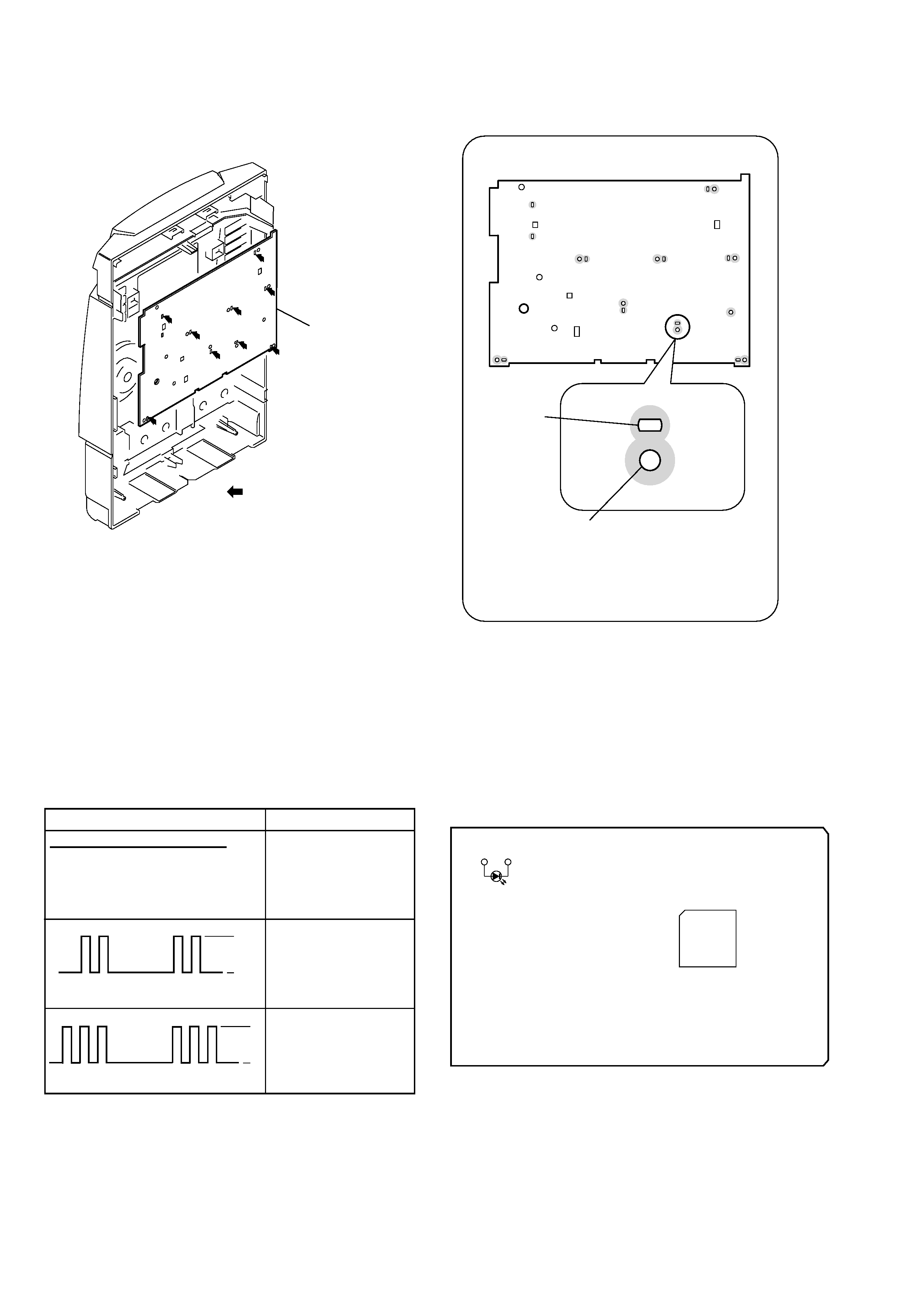
Screw hole
Attach the panel board with
six screws (+BVTP 2.6
× 8 )
after the board is removed once.
Do not tighten the screws excessively.
1
Cut the nine melted-connection points with cutting pliers.
Note for installing the panel board
2
Panel board
Hot melt
: melted-connection point
SELF-DIAGNOSIS
This model has the self-diagnosis function for the VIDEO and AUDIO decoder sections.
Connecting to the LED between TP522 and TP523 on the VIDEO BOARD.
Immediately after the power on, the self-diagnosis function searches each operation of IC's around the CD mechanism control microcom-
puter (IC502). and TP5
The results can be checked by LED of the VIDEO board.
Oscilloscope (Waveform)
Symptom
No error
MPEG decoder (IC505)
error
MPEG decoder (IC505)
or
DRAM (IC507) error
[VIDEO BOARD] (SIDE A)
H
L
Light
2 time blinking
H
L
H
L
3 time blinking
TP523 TP522
LED
IC505
100
91
33
64
90
65
1
32