SERVICE MANUAL
MPEG Layer-3 audio coding technology and
patents licensed from Fraunhofer IIS and
Thomson.
US and foreign patents licensed from Dolby
Laboratories.
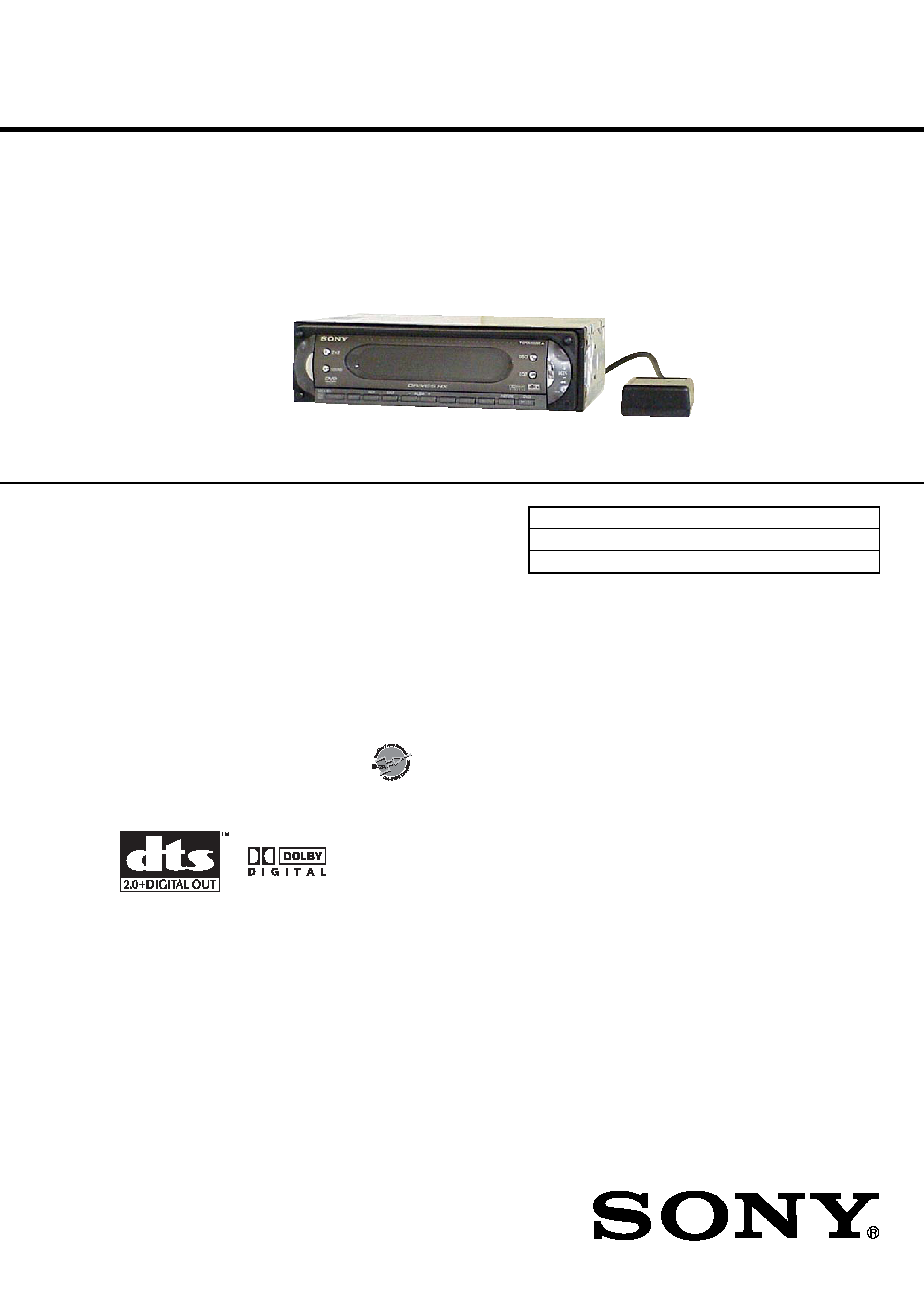
MULTI DISC PLAYER
US Model
Canadian Model
AEP Model
UK Model
E Model
Chinese Model
SPECIFICATIONS
MEX-R5
Ver. 1.2 2005.09
Model Name Using Similar Mechanism
NEW
DVD Mechanism Type
MG-612-187
Optical Pick-up Block Name
KHS-340B
9-879-716-03
2005I05-1
© 2005.09
Sony Corporation
e Vehicle Group
Published by Sony Engineering Corporation
Continued on next page
Copyrights
This product incorporates copyright protection
technology that is protected by U.S. patents and
other intellectual property rights. Use of this
copyright protection technology must be
authorized by Macrovision, and is intended for
home and other limited viewing uses only unless
otherwise authorized by Macrovision. Reverse
engineering or disassembly is prohibited.
Manufactured under license from Dolby
Laboratories.
"Dolby" and the double-D symbol are
trademarks of Dolby Laboratories.
"DTS" and "DTS 2.0 + Digital Out" are
trademarks of Digital Theater Systems, Inc.
System
Laser
Semiconductor laser
Signal format system
NTSC
(US, Canadian models)
PAL
(AEP, UK, Russian models)
PAL/NTSC switchable
(E, Chinese model)
DVD/CD Player section*
Signal-to-noise ratio
120 dB
Frequency response
10 20,000 Hz
Wow and flutter
Below measurable limit
Harmonic distortion (DVD)
0.01%
Wow and flutter
Less than detected value
(
±0.001 % W PEAK)
* Measured from the AUDIO OUT jacks.
When you play PCM sound tracks with a 96 kHz
sampling frequency, the output signals from the
DIGITAL OUT jack are converted to 96 kHz
sampling frequency.
Tuner section
FM
Tuning range
Antenna terminal
External antenna connector
Intermediate frequency
10.7 MHz/450 kHz
Usable sensitivity
9 dBf
Selectivity
75 dB at 400 kHz
Signal-to-noise ratio
67 dB (stereo), 69 dB
(mono)
Harmonic distortion at 1 kHz
0.5 % (stereo),
0.3 % (mono)
Separation
35 dB at 1 kHz
Frequency response
30 15,000 Hz
(US model only)
AUDIO POWER SPECIFICATIONS
POWER OUTPUT AND TOTAL HARMONIC
DISTORTION
23.2 watts per channel minimum continuous
average power into 4 ohms, 4 channels driven
from 20 Hz to 20 kHz with no more than 5% total
harmonic distortion.
CEA2006 Standard
Power Output: 17 Watts RMS
× 4 at
4 Ohms < 1% THD+N
SN Ratio: 82 dBA
(reference: 1 Watt into 4 Ohms)
AEP, UK, Russian,
Asian models:
US, Canadian,
Latin American models:
87.5 107.9 MHz
87.5 108.0 MHz
AM
Tuning range
US, Canadian,
Latin American models:
(at 10 kHz step)
AEP, UK, Russian models:
530 1,710 kHz
MW: 531 1,602 kHz
Asian model:
531 1,602 kHz
LW: 153 279 kHz
(at 9 kHz step)
Antenna terminal
External antenna connector
Intermediate frequency
10.7 MHz/450 kHz
LW: 40
µV
Sensitivity
AM (MW): 30
µV,
· E model and Chinese model are the multi disc player in XMM-R5WL.
2
MEX-R5
Power amplifier section
Outputs
Speaker outputs (sure seal
connectors)
Speaker impedance
4 8 ohms
Maximum power output
52 W
× 4 (at 4 ohms)
(AEP, UK, Russian models)
10 dBm
UK, Russian models)
Wireless AV section
Transmission frequencies 2,414, 2,432, 2,450,
2,468 MHz
Modulation method
FM modulation
RF output power
1.2 dBm (Except AEP,
General
Outputs
Front audio/video output
terminals
Rear audio output terminal
Subwoofer output terminal
(mono)
Optical digital output
terminal
Power antenna relay control
terminal
Power amplifier control
terminal
Inputs
Telephone ATT control
terminal
Illumination control
terminal
BUS control input terminal
BUS audio input/AUX IN
terminal
Parking break control
terminal
Remote controller input
terminal
Antenna input terminal
Tone controls
Bass:
±8 dB at 100 Hz
Treble:
±8 dB at 10 kHz
Loudness
+8 dB at 100 Hz
+2 dB at 10 kHz
Power requirements
12 V DC car battery
(negative ground)
Dimensions
Approx. 178
× 50 × 182 mm
(7 1/8
× 2 × 1/4 in) (w/h/d)
Mounting dimensions
Approx. 182
× 53 × 161 mm
(7 1/4
× 2 1/8 × 6 3/8 in)
(w/h/d)
Mass
Approx. 1.3 kg (2 lb 14 oz)
Supplied accessories
Card remote commander
RM-X704
(US, Canadian models)
RM-X702 (E, Chinese model)
RM-X703
(AEP, UK, Russian models)
Parts for installation and
connections (1 set)
Front panel case (1)
Note
This unit cannot be connected to a digital preamplifier
or an equalizer which is Sony BUS system compatible.
Design and specifications are subject to change
without notice.
Notes on chip component replacement
· Never reuse a disconnected chip component.
· Notice that the minus side of a tantalum capacitor may be
damaged by heat.
Flexible Circuit Board Repairing
· Keep the temperature of the soldering iron around 270 °C
during repairing.
· Do not touch the soldering iron on the same conductor of the
circuit board (within 3 times).
· Be careful not to apply force on the conductor when soldering
or unsoldering.
CAUTION
Use of controls or adjustments or performance of procedures
other than those specified herein may result in hazardous radiation
exposure.
CAUTION
The use of optical instruments with this
product will increase eye hazard.
CAUTION :CLASS 1M VISIBLE/INVISIBLE LASER
RADIATION WHEN OPEN AND INTERLOCKS DEFEATED.
DO NOT VIEW DIRECTLY WITH OPTICAL INSTRUMENTS.
This label is located on the drive unit's internal
chassis
This label is located on the bottom of the
chassis.
CAUTION
Laser radiation when open.
DO NOT STARE INTO BEAM.
-
This label is located on the drive unit's internal
chassis.
ATTENTION AU COMPOSANT AYANT RAPPORT
À LA SÉCURITÉ!
LES COMPOSANTS IDENTIFIÉS PAR UNE MARQUE 0 SUR
LES DIAGRAMMES SCHÉMATIQUES ET LA LISTE DES
PIÈCES
SONT
CRITIQUES
POUR
LA
SÉCURITÉ
DE
FONCTIONNEMENT. NE REMPLACER CES COM- POSANTS
QUE PAR DES PIÈCES SONY DONT LES NUMÉROS SONT
DONNÉS DANS CE MANUEL OU DANS LES SUPPLÉMENTS
PUBLIÉS PAR SONY.
SAFETY-RELATED COMPONENT WARNING!!
COMPONENTS IDENTIFIED BY MARK 0 OR DOTTED LINE
WITH MARK 0 ON THE SCHEMATIC DIAGRAMS AND IN
THE PARTS LIST ARE CRITICAL TO SAFE OPERATION.
REPLACE THESE COMPONENTS WITH SONY PARTS WHOSE
PART NUMBERS APPEAR AS SHOWN IN THIS MANUAL OR
IN SUPPLEMENTS PUBLISHED BY SONY.
US, Canadian models
Ver. 1.1

3
MEX-R5
TABLE OF CONTENTS
1.
SERVICING NOTES ............................................... 4
2.
GENERAL ................................................................... 7
3.
DISASSEMBLY
3-1.
Disassembly Flow ........................................................... 12
3-2.
Sub Panel Complete Assy ................................................ 12
3-3.
DVD Mechanism Deck (MG-612-187) ........................... 12
3-4.
MAIN Board, DC Fan (25
× 25) (M901) ........................ 13
3-5.
Chassis (T) Sub Assy ....................................................... 13
3-6.
Roller Arm Assy .............................................................. 14
3-7.
Chassis (OP-DVD) Complete Assy ................................. 14
3-8.
Chassis (OP-DVD) Sub Assy .......................................... 15
3-9.
LE Motor Assy (Loading) (M3) ...................................... 15
3-10. SERVO Board .................................................................. 16
3-11. Front Back Panel (LCD) .................................................. 16
3-12. BASE Board .................................................................... 17
3-13. Display Section ................................................................ 17
3-14. Bracket (Display) ............................................................ 18
3-15. Spring (S) ........................................................................ 18
4.
ELECTRICAL ADJUSTMENTS ......................... 19
5.
DIAGRAMS
5-1.
Block Diagram SERVO Section ................................ 20
5-2.
Block Diagram AUDIO Section ................................ 21
5-3.
Block Diagram MAIN Section .................................. 22
5-4.
Printed Wiring Board
- SERVO Section (1/2) - ............. 24
5-5.
Printed Wiring Boards
- SERVO Section (2/2) - ........... 25
5-6.
Schematic Diagram
- SERVO Section (1/3) -................ 26
6-7.
Schematic Diagram
- SERVO Section (2/3) -................ 27
6-8.
Schematic Diagram
- SERVO Section (3/3) -................ 28
6-9.
Schematic Diagram MAIN Section (1/3) .................. 29
5-10. Schematic Diagram MAIN Section (2/3) .................. 30
5-11. Schematic Diagram MAIN Section (3/3) .................. 31
5-12. Printed Wiring Board
- MAIN Section (1/2) - ............... 32
5-13. Printed Wiring Boards
- MAIN Section (2/2) - ............. 33
5-14. Printed Wiring Board
- BASE Board - .......................... 34
5-15. Schematic Diagram BASE Board ............................. 35
5-16. Printed Wiring Board
- DISPLAY Board - .................... 36
5-17. Schematic Diagram DISPLAY Board ....................... 37
5-18. Printed Wiring Board
- PRESET Board - ...................... 38
5-19. Schematic Diagram PRESET Board ......................... 38
5-20. Printed Wiring Board
- SUB Board - ............................. 39
5-21. Schematic Diagram SUB Board ................................ 39
6.
EXPLODED VIEWS
6-1.
General Section ............................................................... 58
6-2.
Front Panel Section ......................................................... 59
6-3.
DVD Mechanism Deck Section-1 (MG-612-187) .......... 60
6-4.
DVD Mechanism Deck Section-2 (MG-612-187) .......... 61
6-3.
DVD Mechanism Deck Section-3 (MG-612-187) .......... 62
7.
ELECTRICAL PARTS LIST ................................ 63
4
MEX-R5
MODEL IDENTIFICATION
Label indication
Signal format
Region
Part No.
Destination
system
code
NTSC
1
2-631-964-01 US, Canadian models
PAL2
2-631-969-01 AEP, UK models
PAL5
2-638-206-01 Russian model
PAL3
2-634-525-01 E: PAL model
NTSC
4
2-634-528-01 E: NTSC model
PAL6
2-639-072-01 Chinese model
SECTION 1
SERVICING NOTES
The laser diode in the optical pick-up block may suffer electrostatic
break-down because of the potential difference generated by the
charged electrostatic load, etc. on clothing and the human body.
During repair, pay attention to electrostatic break-down and also
use the procedure in the printed matter which is included in the
repair parts.
The flexible board is easily damaged and should be handled with
care.
NOTES ON LASER DIODE EMISSION CHECK
Never look into the laser diode emission from right above when
checking it for adjustment. It is feared that you will lose your sight.
NOTES ON HANDLING THE OPTICAL PICK-UP
BLOCK OR BASE UNIT
UNLEADED SOLDER
Boards requiring use of unleaded solder are printed with the lead-
free mark (LF) indicating the solder contains no lead.
(Caution: Some printed circuit boards may not come printed with
the lead free mark due to their particular size)
: LEAD FREE MARK
Unleaded solder has the following characteristics.
· Unleaded solder melts at a temperature about 40 °C higher
than ordinary solder.
Ordinary soldering irons can be used but the iron tip has to be
applied to the solder joint for a slightly longer time.
Soldering irons using a temperature regulator should be set to
about 350 °C.
Caution: The printed pattern (copper foil) may peel away if
the heated tip is applied for too long, so be careful!
· Strong viscosity
Unleaded solder is more viscou-s (sticky, less prone to flow)
than ordinary solder so use caution not to let solder bridges
occur such as on IC pins, etc.
· Usable with ordinary solder
It is best to use only unleaded solder but unleaded solder may
also be added to ordinary solder.
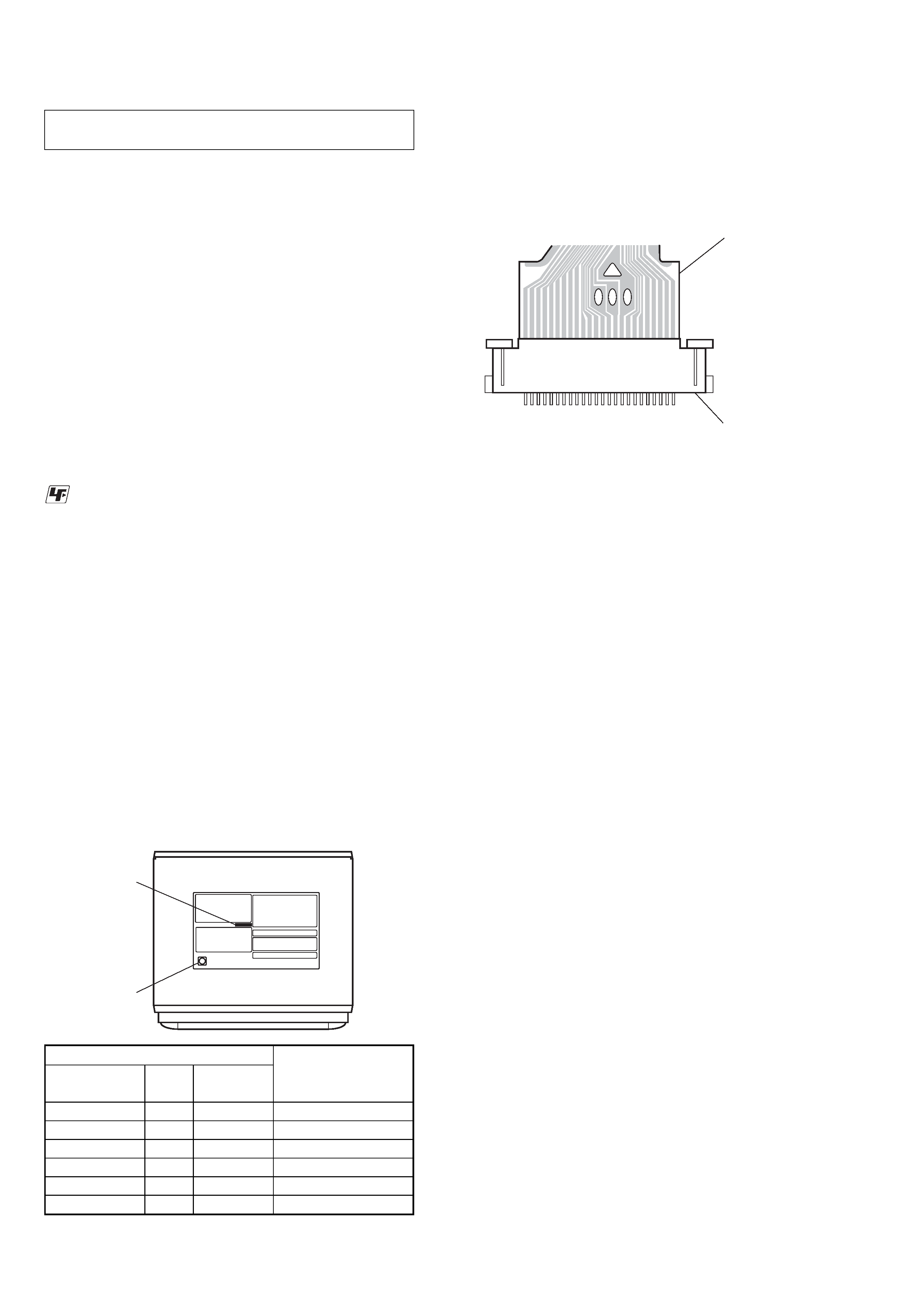
NOTE FOR FLEXIBLE BOARD OF THE OPTICAL
PICK-UP
When connecting or disconnecting the flexible board of the optical
pick-up to or from the CN2 of the SERVO board, follow the
procedure given below.
Figure 1
Note: When soldering the short lands, solder within 5 seconds at the
temperature of soldering iron below 300
°C.
Disconnection:
1. Solder the lands 3 and 2 to short.
2. Solder the lands 1 and 2 to short.
3. Disconnect the flexible board. (Unsolder the shorted lands)
Connection:
1. Make sure that the lands 1, 2, and 3 of the flexible board to be
connected are soldered to short. (*1)
2. Connect the flexible board to the CN2 of the SERVO board.
3. Unsolder the lands 1 and 2. (*2)
4. Unsolder the lands 3 and 2. (*2)
5. Make sure that the respective lands are open surely.
*1)
If the lands concerned are not soldered to short, first solder the lands
3 and 2, and then lands 1 and 2 to short in this order.
*2)
When unsoldering the lands, move the soldering iron in bottom to
top direction in Figure 1 so that the solder runs away into the land 4
(solder reservoir) for easy unsoldering.
NOTE FOR OPERATION CHECK WITH THE BASE
BOARD DISCONNECTED
This set detects whether the front panel is opened or closed by using
the S961 of the BASE board. If the BASE board is disconnected,
the S961 is turned off (panel closed status) and the disc is not ejected.
To perform the disc ejecting operation with the BASE board
disconnected, turn on the S961.
NOTE FOR REPLACING THE MOUNTED MAIN
BOARD
If the mounted MAIN board was replaced, be sure refer to Technical
News published separately.
Bottom View
Part Number
Region Code
4
2
1
Flexible board of
the optical pick-up
SERVO board CN2
3
Ver. 1.1
5
MEX-R5
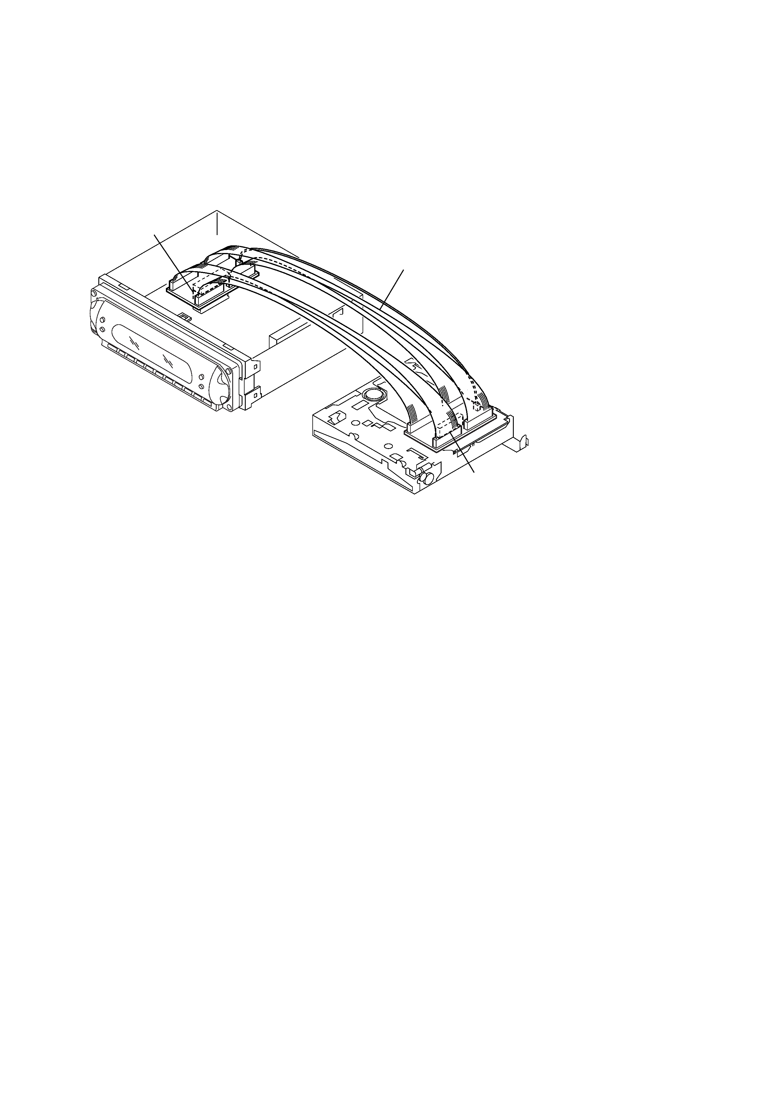
EXTENSION CABLE AND SERVICE POSITION
When repairing or servicing this set, connect the jig (extension cable)
as shown below.
· Connect the MAIN board (CN101) and the SERVO board
(CN3) with the extension cable (Part No. J-2502-094-1).
SERVO board
(CN3)
MAIN board
(CN101)
extension cable
(Part No. J-2502-094-1)