1
Model Name Using Similar Mechanism
NEW
Mini Disc Mechanism Type
MG-164NZ-138
Optical Pick-up Name
KMS-241C/J1NP
SERVICE MANUAL
US Model
Canadian Model
E Model
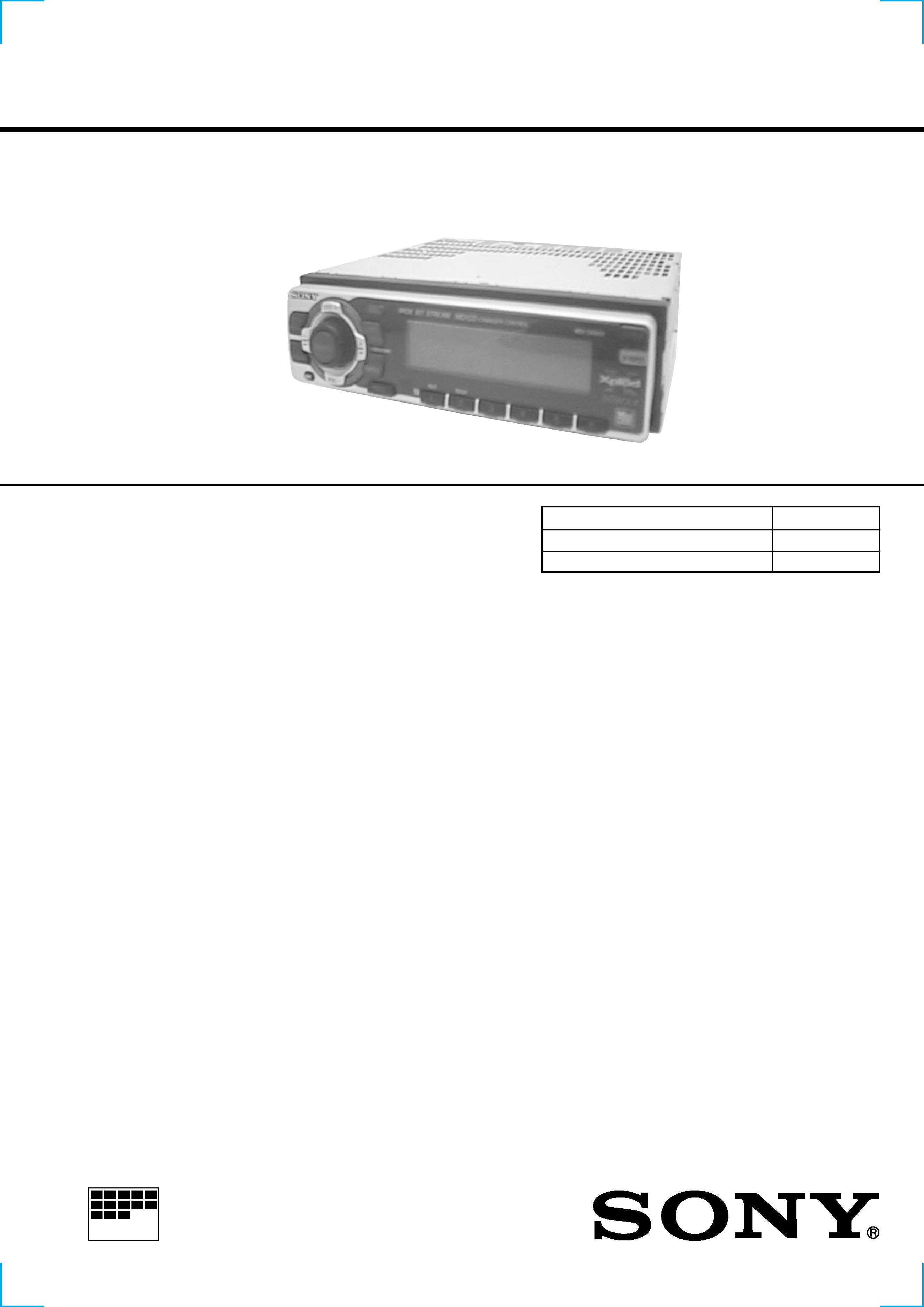
MDX-C6500X
FM/AM MINIDISC PLAYER
MICROFILM
· The tuner and MD sections have no adjustments.
AUDIO POWER SPECIFICATIONS (US Model)
POWER OUTPUT AND TOTAL HARMONIC DISTORTION
19 watts per channel minimum continuous average power into
4 ohms, 4 channels driven from 20 Hz to 20 kHz with no more
than 1% total harmonic distortion.
Other Specifications
MD player section
Signal-to-noise ratio
90 dB
Frequency response
10 20,000 Hz
Wow and flutter
Below measurable limit
Laser Diode Properties
Material
GaAlAs
Wavelength
780 nm
Emission Duration
Continuous
Laser output power
Less than 44.6 µW*
* This output is the value measured at a distance
of 200 mm from the objective lens surface on the
Optical Pick-up Block.
Tuner section
FM
Tuning range
US, Canadian model:
87.5 107.9 MHz
E model:
FM tuning interval:
50 kHz/200 kHz switchable
87.5 108 MHz
(at 50 kHz step)
87.5 107.9 MHz
(at 200 kHz step)
Antenna terminal
External antenna connector
Intermediate frequency 10.7 MHz/450 kHz
Usable sensitivity
8 dBf
Selectivity
75 dB at 400 kHz
Signal-to-noise ratio
66 dB (stereo),
72 dB (mono)
SPECIFICATIONS
Harmonic distortion at 1 kHz
0.6% (stereo),
0.3% (mono)
Separation
35 dB at 1 kHz
Frequency response
30 15,000 Hz
AM
Tuning range
US, Canadian model:
530 1,710 kHz
E model:
AM tuning interval:
9 kHz/10 kHz switchable
531 1,602 kHz
(at 9 kHz step)
530 1,710 kHz
(at 10 kHz step)
Antenna terminal
External antenna connector
Intermediate frequency 10.7 MHz/450 kHz
Sensitivity
30 µV
Continued on next page
Dolby noise reduction extension manufactured under license
from Dolby Laboratories Licensing Corporation.
"DOLBY" and the double-D symbol ; are trademarks of Dolby
Laboratories Licensing Corporation.
2
laser-tap
SAFETY-RELATED COMPONENT WARNING!!
COMPONENTS IDENTIFIED BY MARK 0 OR DOTTED LINE
WITH MARK 0 ON THE SCHEMATIC DIAGRAMS AND IN
THE PARTS LIST ARE CRITICAL TO SAFE OPERATION.
REPLACE THESE COMPONENTS WITH SONY PARTS WHOSE
PART NUMBERS APPEAR AS SHOWN IN THIS MANUAL OR
IN SUPPLEMENTS PUBLISHED BY SONY.
ATTENTION AU COMPOSANT AYANT RAPPORT
À LA SÉCURITÉ!!
LES COMPOSANTS IDENTIFIÉS PAR UNE MARQUE 0 SUR LES
DIAGRAMMES SCHÉMATIQUES ET LA LISTE DES PIÈCES
SONT CRITIQUES POUR LA SÉCURITÉ DE FONCTIONNEMENT.
NE REMPLACER CES COMPOSANTS QUE PAR DES PIÈCES
SONY DONT LES NUMÉROS SONT DONNÉS DANS CE MANUEL
OU DANS LES SUPPLÉMENTS PUBLIÉS PAR SONY.
Notes on Chip Component Replacement
· Never reuse a disconnected chip component.
· Notice that the minus side of a tantalum capacitor may be dam-
aged by heat.
CAUTION
Use of controls or adjustments or performance of procedures
other than those specified herein may result in hazardous ra-
diation exposure.
Power amplifier section
Outputs
Speaker outputs
(sure seal connectors)
Speaker impedance
4 8 ohms
Maximum power output 50 W
× 4 (at 4 ohms)
General
Outputs
Audio outputs
Power antenna relay
control lead
Power amplifier control
lead
Telephone ATT control
lead
Tone controls
Bass ±9 dB at 100 Hz
Treble ±9 dB at 10 kHz
Power requirements
12 V DC car battery
(negative ground)
Dimensions
Approx. 178
× 50 × 183 mm
(7 1/8
× 2 × 7 1/4 in.)
(w/h/d)
Mounting dimensions
Approx. 182
× 53 × 162 mm
(7 1/4
× 2 1/8 × 6 1/2 in.)
(w/h/d)
Mass
Approx. 1.2 kg (2 lb. 10 oz.)
Supplied accessories
Parts for installation and
connections (1 set)
Front panel case (1)
Design and specifications are subject to change without
notice.
Flexible Circuit Board Repairing
· Keep the temperature of the soldering iron around 270 °C dur-
ing repairing.
· Do not touch the soldering iron on the same conductor of the
circuit board (within 3 times).
· Be careful not to apply force on the conductor when soldering
or unsoldering.
The laser diode in the optical pick-up block may suffer electrostatic
break-down because of the potential difference generated by the
charged electrostatic load, etc. on clothing and the human body.
During repair, pay attention to electrostatic break-down and also
use the procedure in the printed matter which is included in the
repair parts.
The flexible board is easily damaged and should be handled with
care.
NOTES ON LASER DIODE EMISSION CHECK
Never look into the laser diode emission from right avove when
checking it for adustment. It is feared that you will lose your sight.
NOTES ON HANDLING THE OPTICAL PICK-UP BLOCK
(KMS-241C/J1NP)
The laser diode in the optical pick-up block may suffer electrostatic
break-down easily. When handling it, perform soldering bridge to
the laser-tap on the flexible board. Also perform m easures against
electrostatic break-down sufficiently before the operation. The flex-
ible board is easily damaged and should be handled with care.
OPTICAL PICK-UP FLEXIBLE BOARD
NOTES ON HANDLING THE OPTICAL PICK-UP
BLOCK OR BASE UNIT

3
TABLE OF CONTENTS
1. GENERAL
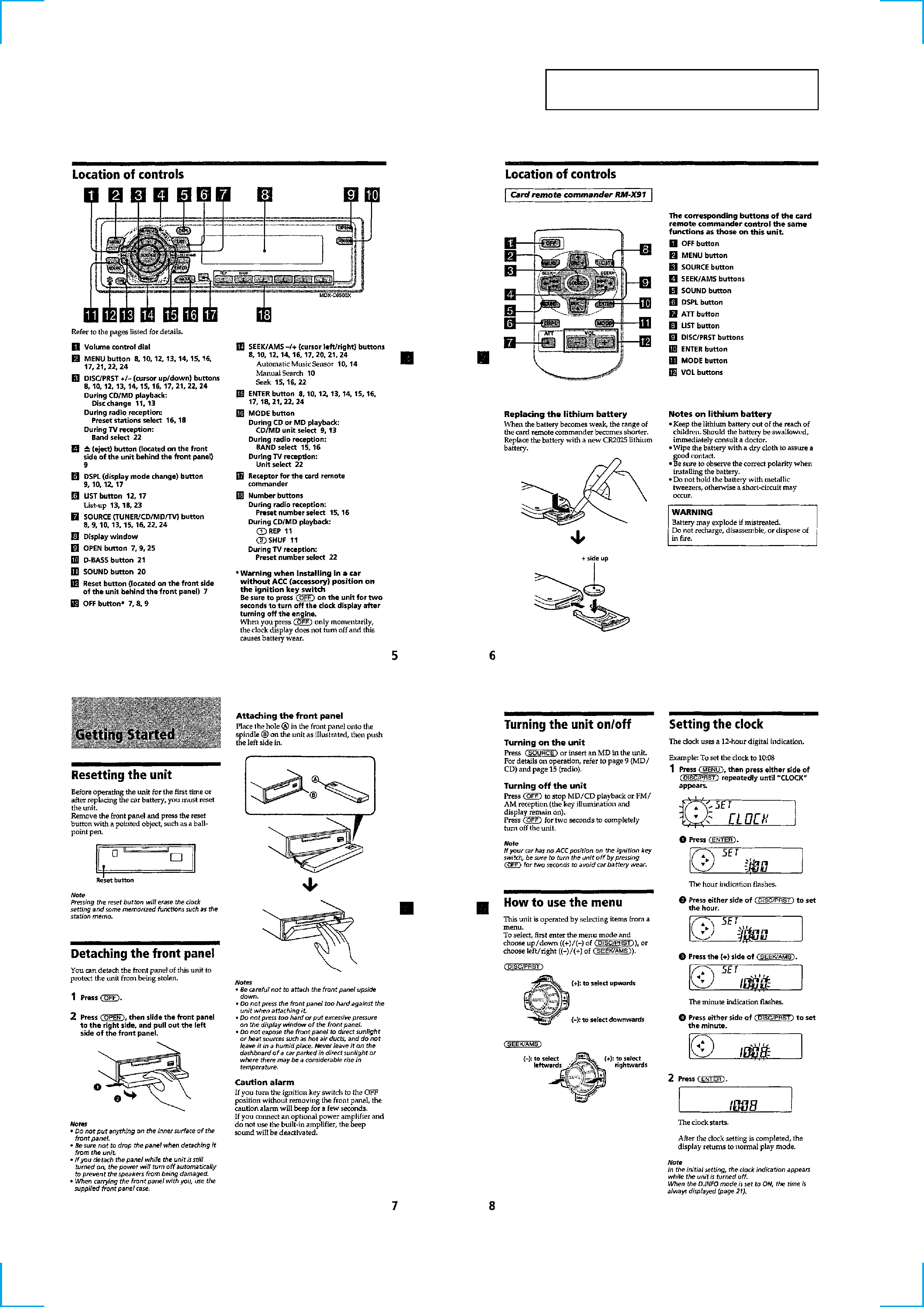
Location of Controls ................................................................ 4
Getting Started ......................................................................... 4
Setting the Clock ..................................................................... 4
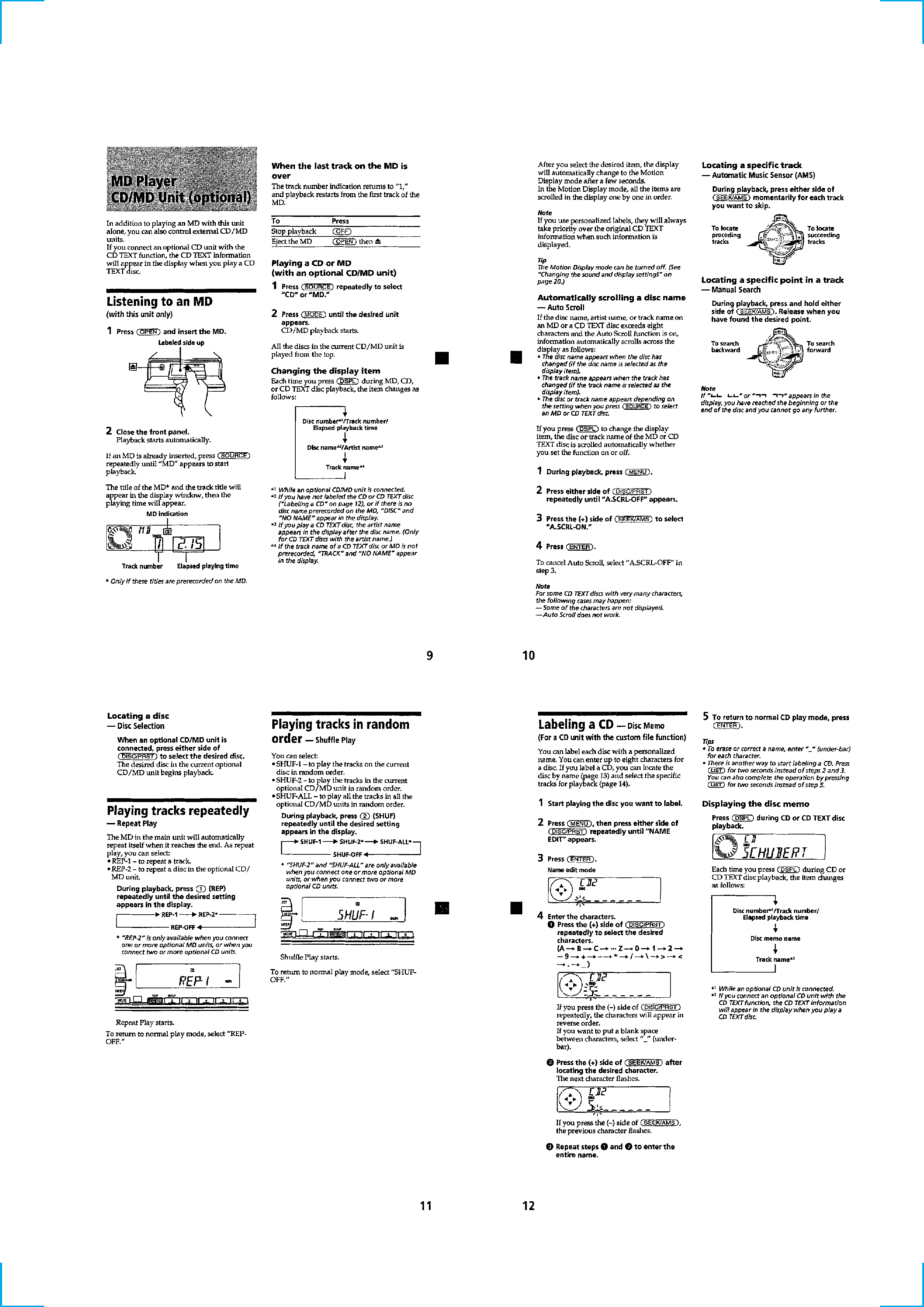
MD Player CD/MD Unit (optional) ........................................ 5
Radio ....................................................................................... 6
Other Functions ....................................................................... 7
TV/Video (optional) ................................................................ 8
Additional Information ............................................................ 8
Connections ........................................................................... 10
2. DISASSEMBLY
2-1. Sub Panel (MD) Assy ........................................................ 12
2-2. MD Mechanism Block ...................................................... 12
2-3. Main Board ....................................................................... 13
2-4. Heat Sink ........................................................................... 13
2-5. Servo Board ....................................................................... 14
2-6. MD Cover Assy ................................................................. 14
2-7. Float Block ........................................................................ 15
2-8. Lo Motor Assy (Loading) (M903) .................................... 15
2-9. Lever Assy (LE) ................................................................ 16
2-10. Holder Assy ....................................................................... 16
2-11. Chucking Arm Assy .......................................................... 17
2-12. Optical Pick-up (KMS-241C/J1RP) ................................. 17
2-13. SL Motor Assy (Sled) (M902)
/SP Motor Assy (Spindle) (M901) .................................... 18
3. DIAGRAMS
3-1. IC Pin Descriptions ........................................................... 19
3-2. Block Diagram MD Section .......................................... 27
3-3. Block Diagram Tuner Section ....................................... 28
3-4. Block Diagram Display Section .................................... 29
3-5. Circuit Boards Location .................................................... 29
3-6. Printed Wiring Board MD Mechanism Section ............ 31
3-7. Schematic Diagram MD Mechanism Section (1/2) ...... 32
3-8. Schematic Diagram MD Mechanism Section (2/2) ...... 33
3-9. Schematic Diagram Main Section (1/2) ........................ 34
3-10. Schematic Diagram Main Section (2/2) ........................ 35
3-11. Printed Wiring Board Main Section .............................. 36
3-12. Printed Wiring Board Relay Section ............................. 37
3-13. Schematic Diagram Relay Section ................................ 38
3-14. Schematic Diagram Display Section ............................. 39
3-15. Printed Wiring Board Display Section .......................... 40
3-16. IC Block Diagrams ............................................................ 41
4. EXPLODED VIEWS
4-1. Chassis Section ................................................................. 46
4-2. Front Panel Section ........................................................... 47
4-3. MD Mechanism Section (1) .............................................. 48
4-4. MD Mechanism Section (2) .............................................. 49
5. ELECTRICAL PARTS LIST ........................................ 50
4
SECTION 1
GENERAL
This section is extracted from
US, Canadian model's instruction manual.
5