Ver 1.0
1998.06
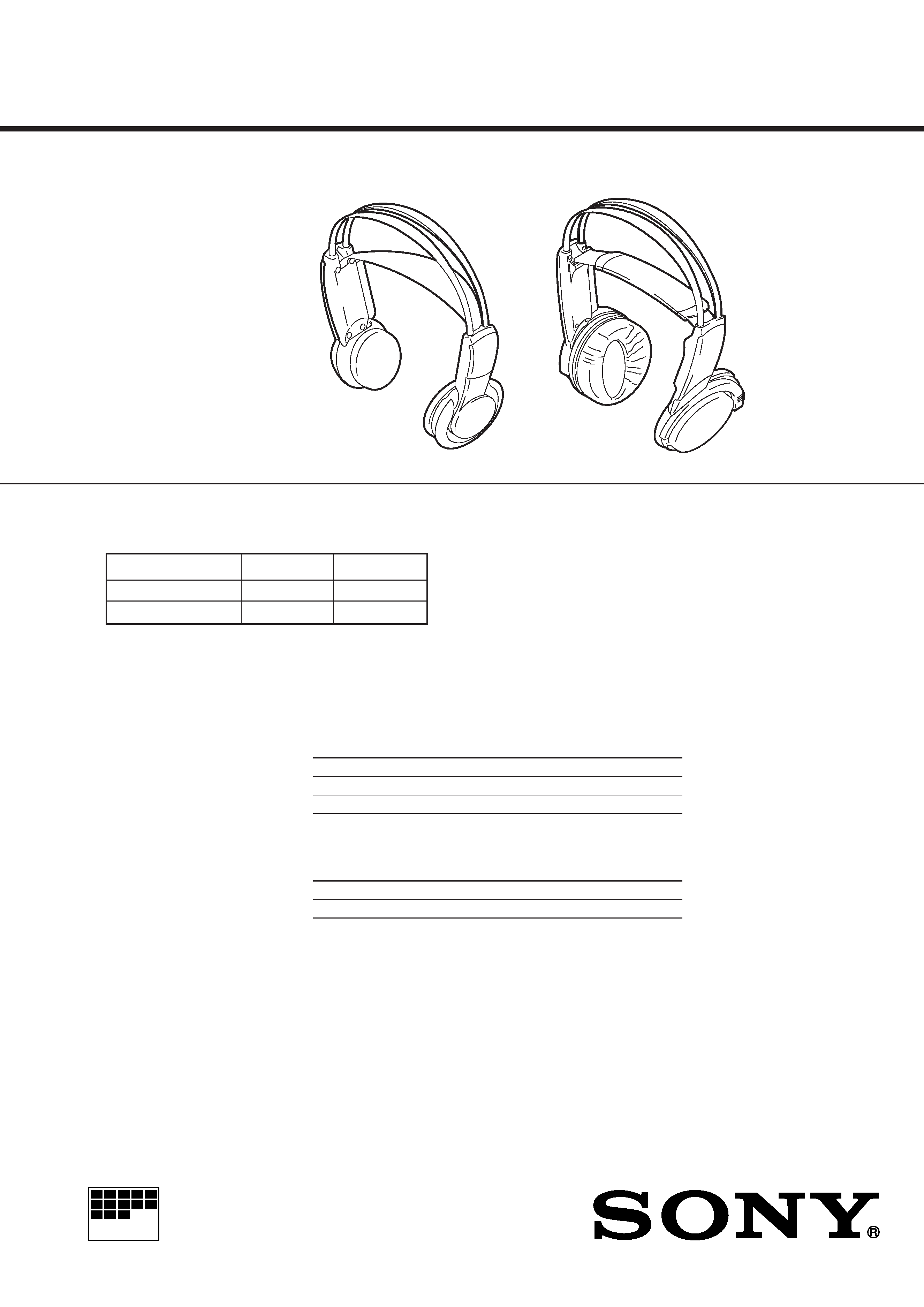
Headphone
Charging and using hours
Approx. charging hours
Approx. using time*
1
50 minutes
24**
20 hours
*
at 1kHz 1mW + 1mW output
** the hours required to fully charge empty batteries
Battery life
Battery
Approx. hours*
Sony alkaline battery LR6 (SG) 60
Sony battery R6P (SR)
30
*
at 1kHz 1mW + 1mW output
Power source
DC 3V : 2 x R6 (size AA) battery or 2 x supplied
NC-AA-HJ Ni-Cd rechargeable battery
Mass
Approx. 215g (7.6oz.) incl.Ni-Cd batteries (MDR-RF430RK)
Approx. 265g (9.4oz.) incl.Ni-Cd batteries (MDR-RF450RK)
Supplied Ni-Cd rechargeable batteries
Model name
NC-AA-HJ
Voltage
1.2V
Capacity
600mAh
Design and specifications are subject to change without notice.
MICROFILM
MDR-RF430/RF450
SERVICE MANUAL
WIRELESS STEREO HEADPHONES
AEP Model
MDR-RF430RK MDR-RF450RK
Wireless Headphones
MDR-RF430
MDR-RF450
Transmitter
TMR-RF450R
TMR-RF450R
COMPONENT MODEL NAME FOR MDR-RF430RK/RF450RK
SPECIFICATIONS
MDR-RF430 is the component model block one in the MDR-RF430RK.
MDR-RF450 is the component model block one in the MDR-RF450RK.
Illustration : MDR-RF430
Illustration : MDR-RF450
2
SECTION 1
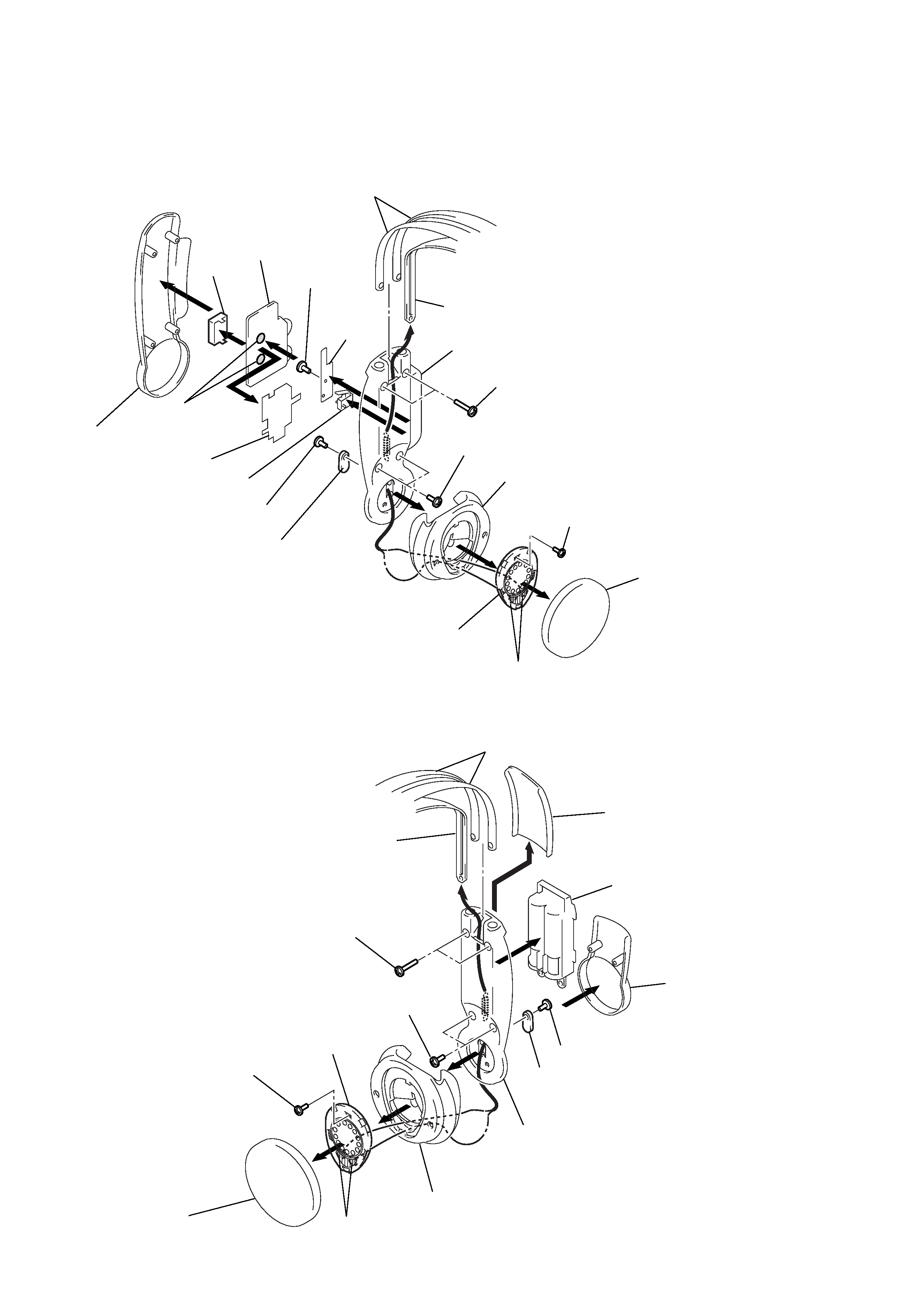
DISASSEMBLY
Note:Followthedisassemblyprocedureinthenumericalordergiven.
1-1. RX BOARD, FE BOARD, RECEIVER (R-CH), SUSPENDER REMOVAL
1-2. BATTERY CASE, RECEIVER (L-CH), SUSPENDER REMOVAL
MDR-RF430
2 Screws +P 2x10
9 Screw
(M1.7x4)
!TM Screw
+P 2x6
3 Screws +P 2x5
!¢Screw (M 1.7x4)
7 Remove
solder
RX shield plate
!§ Remove solder
Hanger cover (R)
Spacer
Hanger (R)
Suspender
Head band
5 RX board
Housing (R) assy
MDD02 (R-CH)
SW1
Ball shaft holder
Ear pad
!¡
!¶
1
!
!£
4
8
6
!º
FE board
2 Screws +P 2x10
7 Screw +P 2x6
3 Screws +P 2x5
!¡ Remove solder
Hanger cover (L)
Suspender
Head band
Battery cover
Battery case
Housing (L) assy
Hanger (L)
MDD01 (L-CH)
Ball shaft holder
Ear pad
9 Screw (M 1.7x4)
1
!º
4
6
!TM
8
5
3
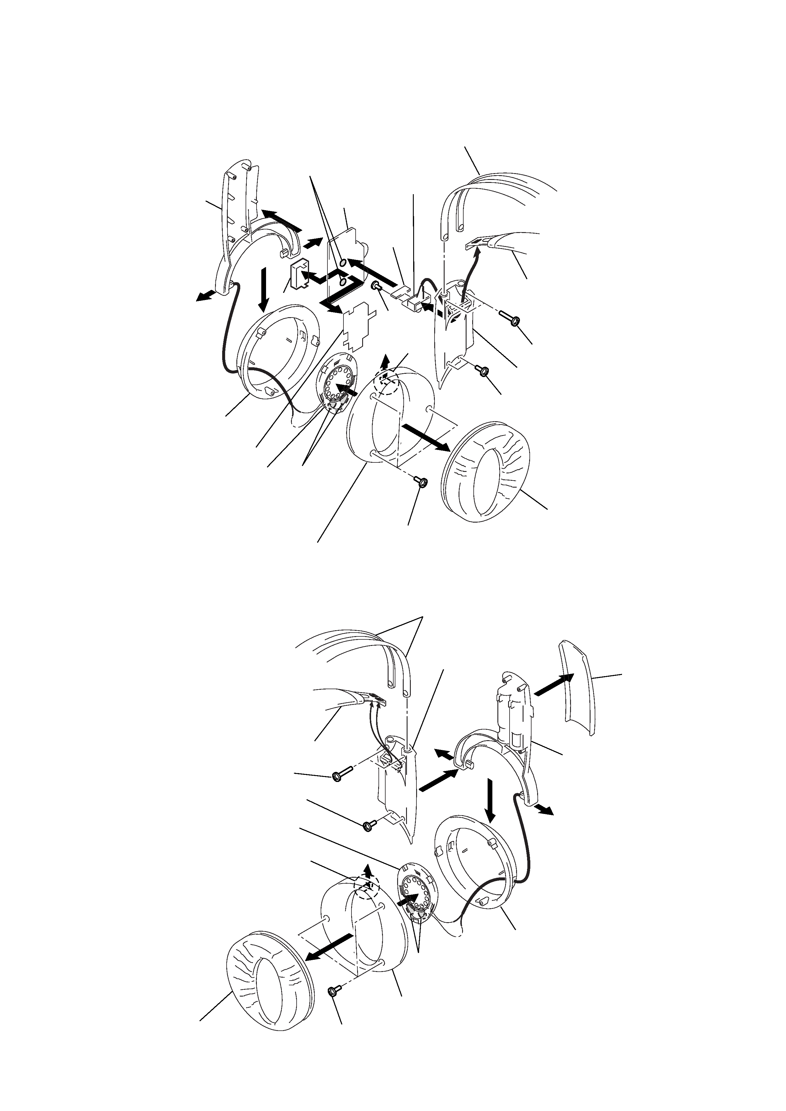
1-1. RECEIVER (R-CH), RX BOARD, FE BOARD, SUSPENDER ASSY REMOVAL
1-2. RECEIVER (L-CH), SUSPENDER ASSY REMOVAL
MDR-RF450
Hanger (R)
Hanger cover (R)
Housing (R)
!£ Remove
solder
3 Remove
solder
0
9
5
4
1
9
!¢
!¡
!
!§
!TM
8
!¶ SW
board
Surpport switch
MDD02 (R-CH)
RX shield plate
Claw
2 Screws
(M 1.7x4)
Ear pad
7 Screws (M1.7x4)
6 Screws +P 2x8
Front plat (R) assy
Screw
(M1.7x4)
RX board
FE board
Head band
Suspender
Ear pad
2 Screws
(M 1.7x5) tapping
0 Screws (M 1.7x4)
Head band
Hanger cover (L)
Suspender
3 Remove solder
MDD01 (L-CH)
9Screws +P 2x8
Front plate (L) assy
Claw
Housing (L)
Hanger (L)
Battery cover
5
1
!TM
6
!¡
8
7
6
4
4
SECTION 2
ELECTRICAL ADJUSTMENTS
Separation check and adjustment
1.
SetthetransmitterchanneltoCH2.
2.
SetthetransmitternoisefilterSWtoOFF
.
3.
Inputasignalof1kHz316mVrmstoonl
ythetransmitterL-c
h
(J403).
4.
Connectandigitalvoltmeter(ACrange)andoscilloscopeto
theL-chspeakeroutputs(bothsidesofMDD01).
5.
Receive signals b
y turning the
TUNINGVOL (RV302).
6.
Adjust the VOL (RV301) so that the RX boar
d L-c h speaker
outputs(bothsidesofMDD01)are155mVrms.
7.
Connectandigitalvoltmeter(ACrange)andoscilloscopeto
theR-chspeakeroutputs(bothsidesofMDD02)andmeasure
thevoltages.
8.
Atthistime,checktomakesurethelevelseparationofL-ch
andR-chspeakeroutputsismorethan20dB.Iftheseparation
islessthan20dB,
turnR V303ontheRXboar
dsothattheR-c
h
outputisminimal,thenchecktoseeifthelevelseparationofL-
chandR-chspeakeroutputsismorethan20dB.
9.
Inputasignalof1kHz316mVrmstoonl
ythetransmitterR-c
h
(J402).
10. Adjust the VOL (RV301) so that the RX boar
d R-c h speaker
outputs(bothsidesofMDD02)are155mVrms.
11. Connectandigitalvoltmeter(ACrange)andoscilloscopeto
theL-chspeakeroutputs(bothsidesofMDD01)andmeasure
thevoltages.
12. Atthistime,checktomakesurethelevelseparationofL-ch
andR-chspeakeroutputsismorethan20dB.
Receive frequency check and adjustment
1. SetthetransmitterchanneltoCH2.
2. SetthetransmitternoisefilterSWtoOFF
.
3. Inputasignalof1kHz316mVrmstoonl
ythetransmitterL-c
h
(J403).
4. Placetransmitterandheadphonesatadistanceofmorethan5m
apart.
5. Set the VOL (RV301) to MIN.
6. Position RX boar
d TUNINGVOL (RV302) to the center
.
7. Connectadigitalvoltmeter(DCrange)andanoscilloscopebe-
tween IC301 pin
@¡and GND.
8. Firstchecktomakesurethatademodulatedwaveformof1kHz
(appr oximatel y13mVrms)isoutputtedtotheoscilloscope
,then
chec ktomakesuretheDCv
oltmeterreadingisDC11.2V
.
9. Ifademodulatedwaveformof1kHzisnotoutputtedtotheos-
cilloscope or if the DC level is not within the range specified
above,adjusttheRXboardL301sothatademodulatedwave-
formof1kHzisoutputtedtotheoscilloscopeandwhilethewave-
form is outputted, further fine adjust the L301 so that the DC
voltmeterreadingisDC1.1V
.
10. Whencompleted,makesuresignalscanbereceivedwhenswitch-
ingthetransmitterchanneltoCH1orCH3byturningRXboard
TUNING VOL (RV302).
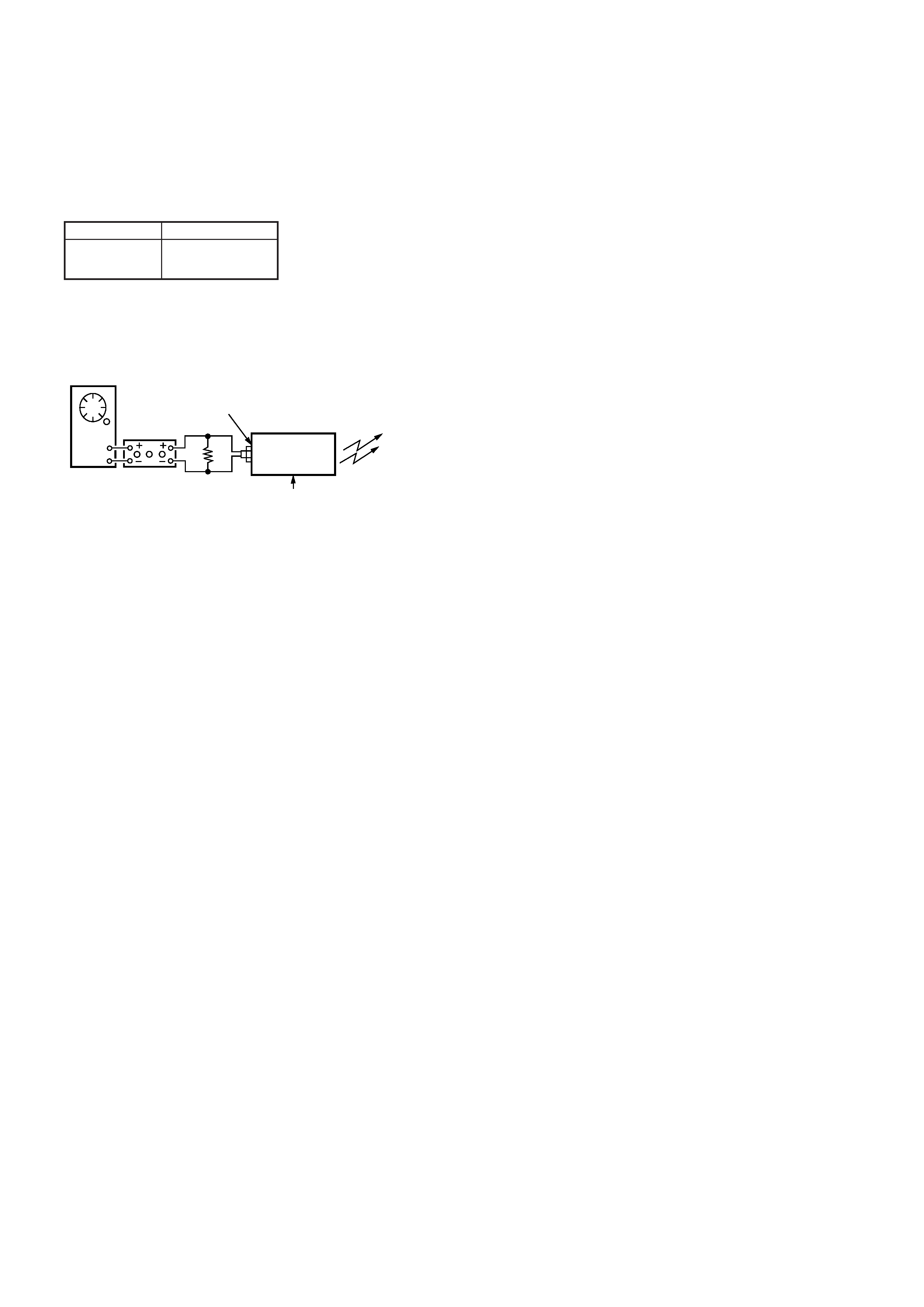
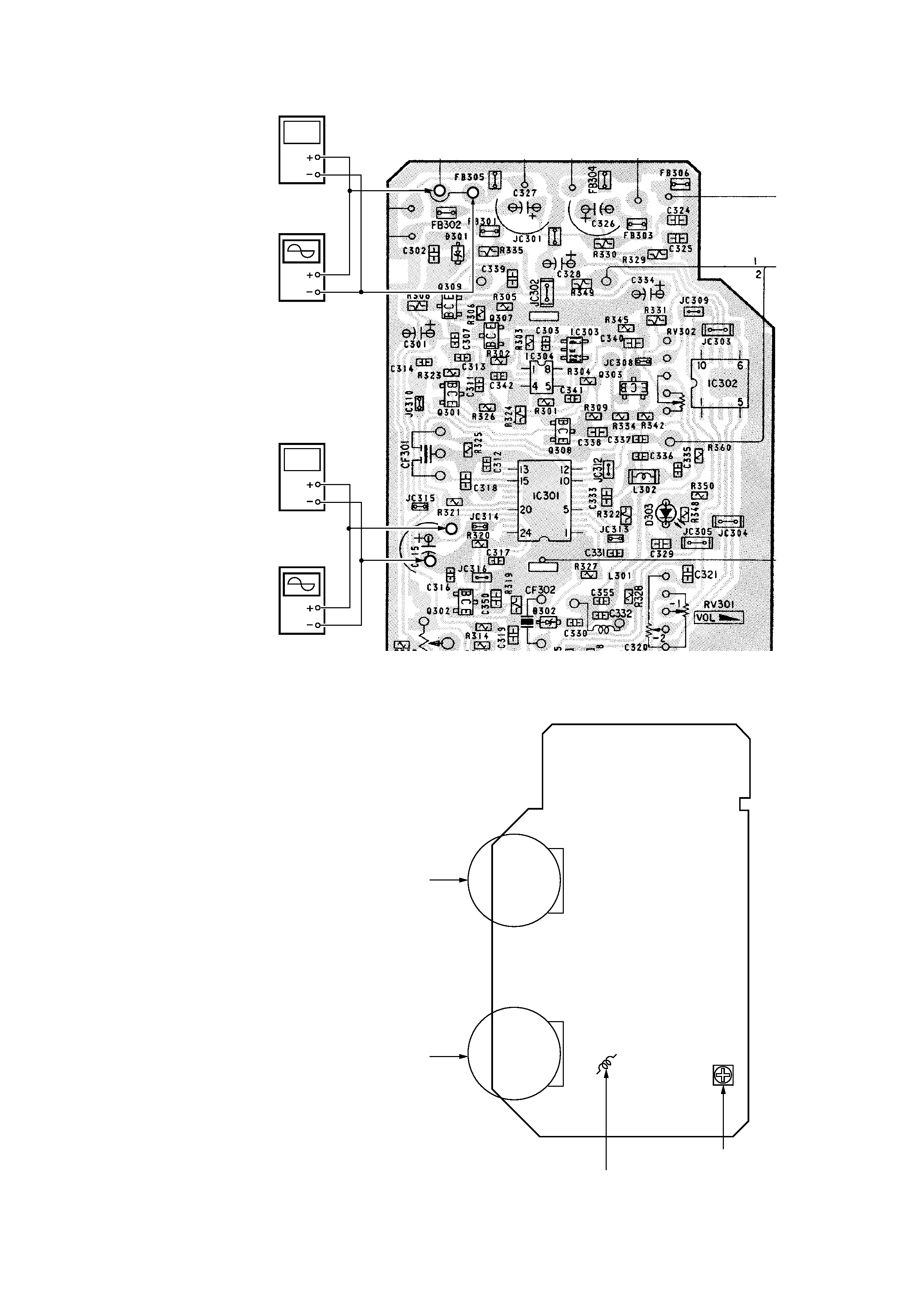
Connection points and Adjustment Location :
RXboard(Seepage5)
Note :
1. Usetransmitterwithcheckandadjustmentalreadycompleted.
2. Thetransmittersectionadjustmentsshouldbecompletedbefore
performingtheheadphonessectionadjustment.
3. Onadjustingtheheadphonessection,usethetransmitterasa
jig.
Headphones
Transmitter
MDR-RF430
TMR-RF450R
MDR-RF450
Setting :
Transmitter
J404
power supply
(DC 11V)
L-CH (J403)
1kHz 316mVrms (7.8dB)
AF OSC
ATT
Jig
600
Connection points and Adjustment Location :
RXboard(Seepage5)
1. Feedasignaltojig(transmitter)andconnectapowersupplyto
DC IN 9V jack (J404).
5
Connection points :
Adjustment Location :
RV302
Tuning Knob
RV301
VOL Knob
L301 : Receive Frequency Adjustment
RV303 : Separation Adjustment
[RX BOARD] (Component side)
[ RX BOARD ] (Conductor side)
oscilloscope
digital voltmeter
(AC range)
oscilloscope
digital voltmeter
(DC range)