Ver 1.1 2000.12
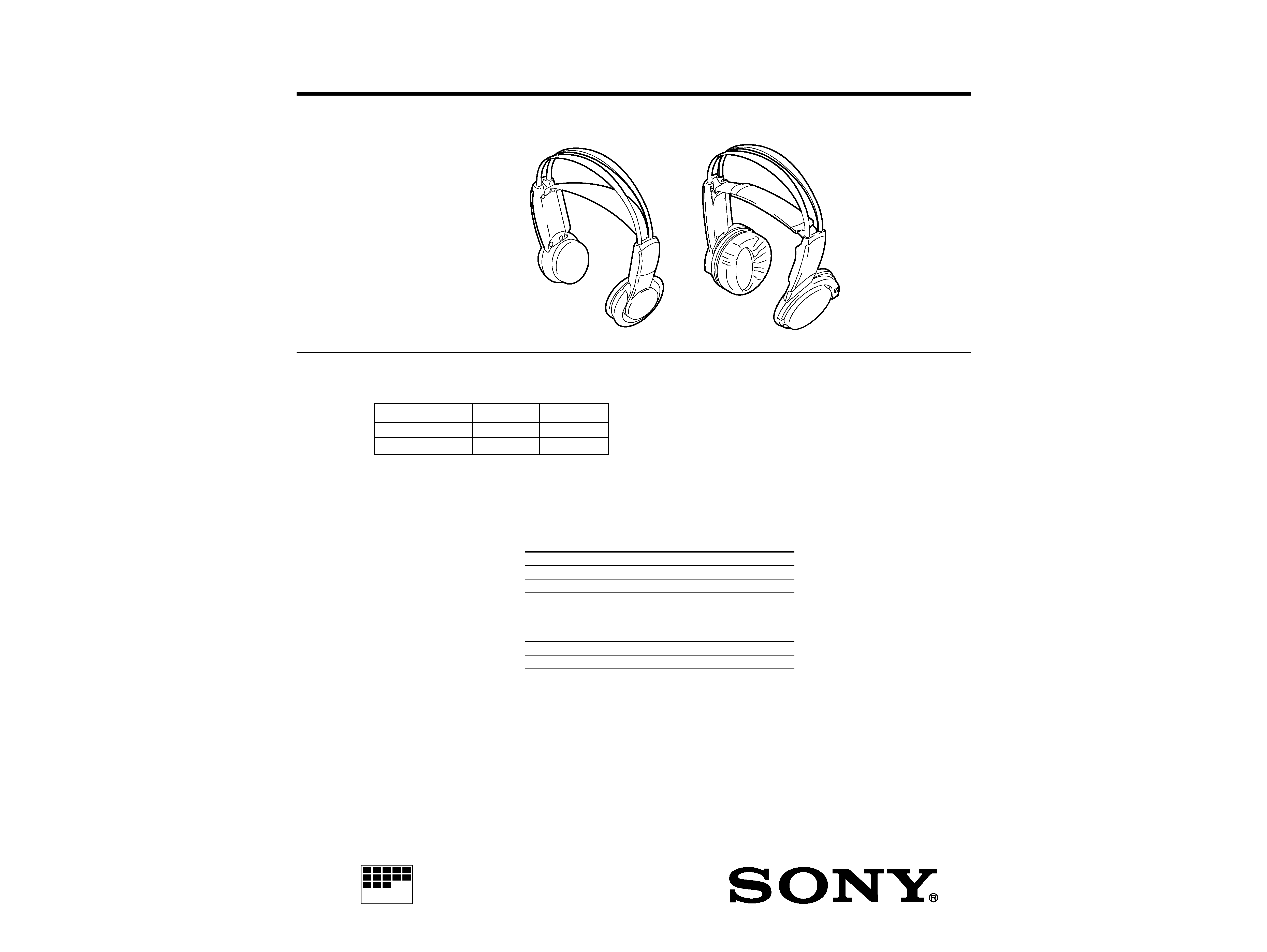
Headphone
Charging and using hours
Approx. charging hours
Approx. using time*
1
50 minutes
24**
20 hours
*
at 1kHz 1mW + 1mW output
** the hours required to fully charge empty batteries
Battery life
Battery
Approx. hours*
Sony alkaline battery LR6 (SG) 60
Sony battery R6P (SR)
30
*
at 1kHz 1mW + 1mW output
Power source
DC 3V : 2 x R6 (size AA) battery or 2 x supplied
NC-AA-HJ Ni-Cd rechargeable battery
Mass
Approx. 215g (7.6oz.) incl.Ni-Cd batteries (MDR-RF430RK)
Approx. 265g (9.4oz.) incl.Ni-Cd batteries (MDR-RF450RK)
Supplied Ni-Cd rechargeable batteries
Model name
NC-AA-HJ
Voltage
1.2V
Capacity
600mAh
Design and specifications are subject to change without notice.
MICROFILM
MDR-RF430/RF450
SERVICE MANUAL
WIRELESS STEREO HEADPHONES
AEP Model
MDR-RF430RK MDR-RF450RK
Wireless Headphones
MDR-RF430
MDR-RF450
Transmitter
TMR-RF450R
TMR-RF450R
COMPONENT MODEL NAME FOR MDR-RF430RK/RF450RK
SPECIFICATIONS
MDR-RF430 is the component model block one in the MDR-RF430RK.
MDR-RF450 is the component model block one in the MDR-RF450RK.
Illustration : MDR-RF430
Illustration : MDR-RF450
2
SECTION 1
DISASSEMBLY
Note:Followthedisassemblyprocedureinthenumericalordergiven.
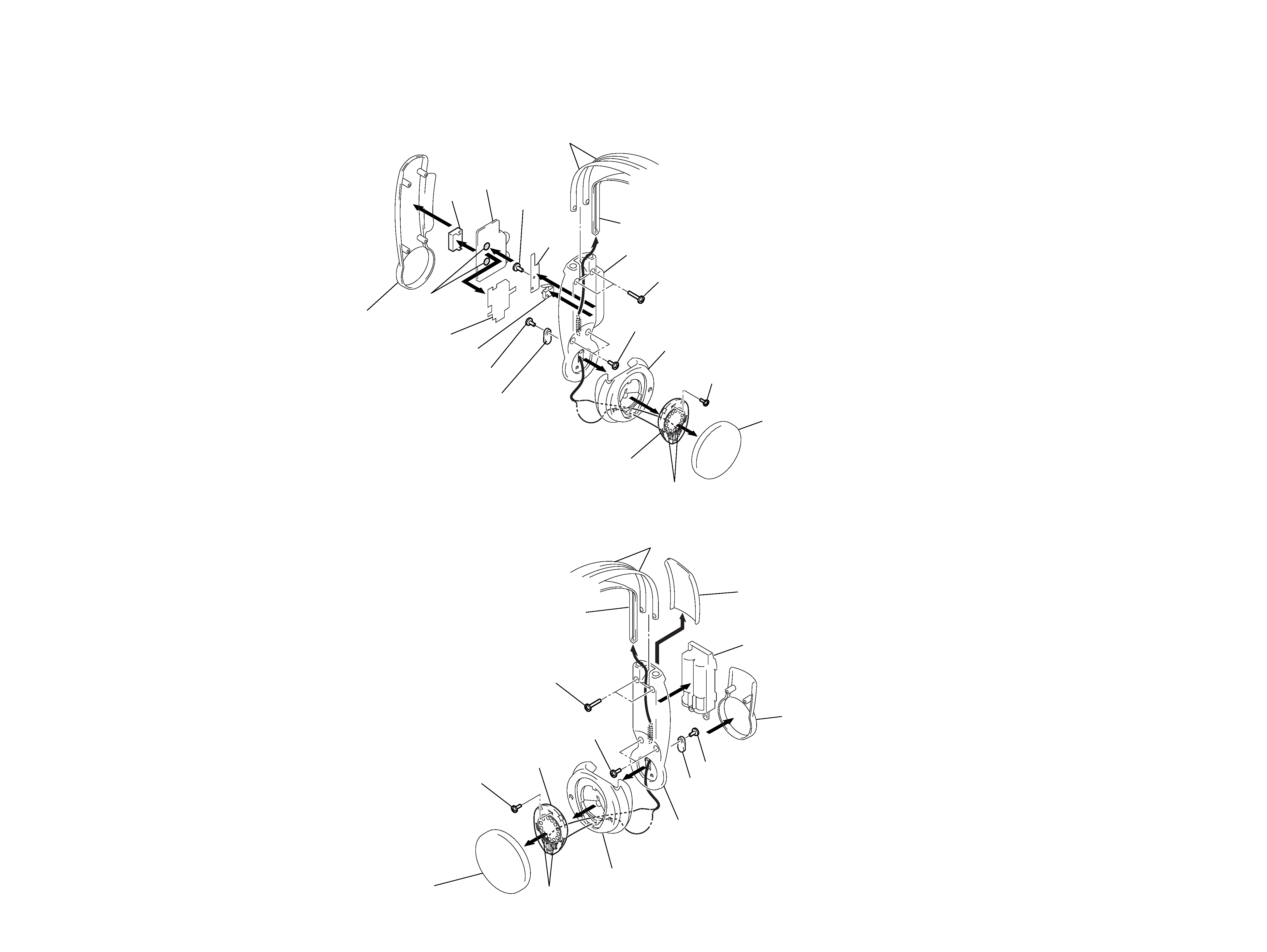
1-1. RX BOARD, FE BOARD, RECEIVER (R-CH), SUSPENDER REMOVAL
1-2. BATTERY CASE, RECEIVER (L-CH), SUSPENDER REMOVAL
MDR-RF430
2 Screws +P 2x10
9 Screw
(M1.7x4)
!TM Screw
+P 2x6
3 Screws +P 2x5
!¢Screw (M 1.7x4)
7 Remove
solder
RX shield plate
!§ Remove solder
Hanger cover (R)
Spacer
Hanger (R)
Suspender
Head band
5 RX board
Housing (R) assy
MDD02 (R-CH)
SW1
Ball shaft holder
Ear pad
!¡
!¶
1
!
!£
4
8
6
!º
FE board
2 Screws +P 2x10
7 Screw +P 2x6
3 Screws +P 2x5
!¡ Remove solder
Hanger cover (L)
Suspender
Head band
Battery cover
Battery case
Housing (L) assy
Hanger (L)
MDD01 (L-CH)
Ball shaft holder
Ear pad
9 Screw (M 1.7x4)
1
!º
4
6
!TM
8
5
3
1-1. RECEIVER (R-CH), RX BOARD, FE BOARD, SUSPENDER ASSY REMOVAL
1-2. RECEIVER (L-CH), SUSPENDER ASSY REMOVAL
MDR-RF450
Hanger (R)
Hanger cover (R)
Housing (R)
!£ Remove
solder
3 Remove
solder
0
9
5
4
1
9
!¢
!¡
!
!§
!TM
8
!¶ SW
board
Surpport switch
MDD02 (R-CH)
RX shield plate
Claw
2 Screws
(M 1.7x4)
Ear pad
7 Screws (M1.7x4)
6 Screws +P 2x8
Front plat (R) assy
Screw
(M1.7x4)
RX board
FE board
Head band
Suspender
Ear pad
2 Screws
(M 1.7x5) tapping
0 Screws (M 1.7x4)
Head band
Hanger cover (L)
Suspender
3 Remove solder
MDD01 (L-CH)
9Screws +P 2x8
Front plate (L) assy
Claw
Housing (L)
Hanger (L)
Battery cover
5
1
!TM
6
!¡
8
7
6
4
4
SECTION 2
ELECTRICAL ADJUSTMENTS
Separation check and adjustment
1.
SetthetransmitterchanneltoCH2.
2.
SetthetransmitternoisefilterSWtoOFF
.
3.
Inputasignalof1kHz316mVrmstoonl
ythetransmitterL-c
h
(J403).
4.
Connectandigitalvoltmeter(ACrange)andoscilloscopeto
theL-chspeakeroutputs(bothsidesofMDD01).
5.
Receive signals b
y turning the
TUNINGVOL (RV302).
6.
Adjust the VOL (RV301) so that the RX boar
d L-c h speaker
outputs(bothsidesofMDD01)are155mVrms.
7.
Connectandigitalvoltmeter(ACrange)andoscilloscopeto
theR-chspeakeroutputs(bothsidesofMDD02)andmeasure
thevoltages.
8.
Atthistime,checktomakesurethelevelseparationofL-ch
andR-chspeakeroutputsismorethan20dB.Iftheseparation
islessthan20dB,
turnR V303ontheRXboar
dsothattheR-c
h
outputisminimal,thenchecktoseeifthelevelseparationofL-
chandR-chspeakeroutputsismorethan20dB.
9.
Inputasignalof1kHz316mVrmstoonl
ythetransmitterR-c
h
(J402).
10. Adjust the VOL (RV301) so that the RX boar
d R-c h speaker
outputs(bothsidesofMDD02)are155mVrms.
11. Connectandigitalvoltmeter(ACrange)andoscilloscopeto
theL-chspeakeroutputs(bothsidesofMDD01)andmeasure
thevoltages.
12. Atthistime,checktomakesurethelevelseparationofL-ch
andR-chspeakeroutputsismorethan20dB.
Receive frequency check and adjustment
1. SetthetransmitterchanneltoCH2.
2. SetthetransmitternoisefilterSWtoOFF
.
3. Inputasignalof1kHz316mVrmstoonl
ythetransmitterL-c
h
(J403).
4. Placetransmitterandheadphonesatadistanceofmorethan5m
apart.
5. Set the VOL (RV301) to MIN.
6. Position RX boar
d TUNINGVOL (RV302) to the center
.
7. Connectadigitalvoltmeter(DCrange)andanoscilloscopebe-
tween IC301 pin
@¡and GND.
8. Firstchecktomakesurethatademodulatedwaveformof1kHz
(appr oximatel y13mVrms)isoutputtedtotheoscilloscope
,then
chec ktomakesuretheDCv
oltmeterreadingisDC11.2V
.
9. Ifademodulatedwaveformof1kHzisnotoutputtedtotheos-
cilloscope or if the DC level is not within the range specified
above,adjusttheRXboardL301sothatademodulatedwave-
formof1kHzisoutputtedtotheoscilloscopeandwhilethewave-
form is outputted, further fine adjust the L301 so that the DC
voltmeterreadingisDC1.1V
.
10. Whencompleted,makesuresignalscanbereceivedwhenswitch-
ingthetransmitterchanneltoCH1orCH3byturningRXboard
TUNING VOL (RV302).
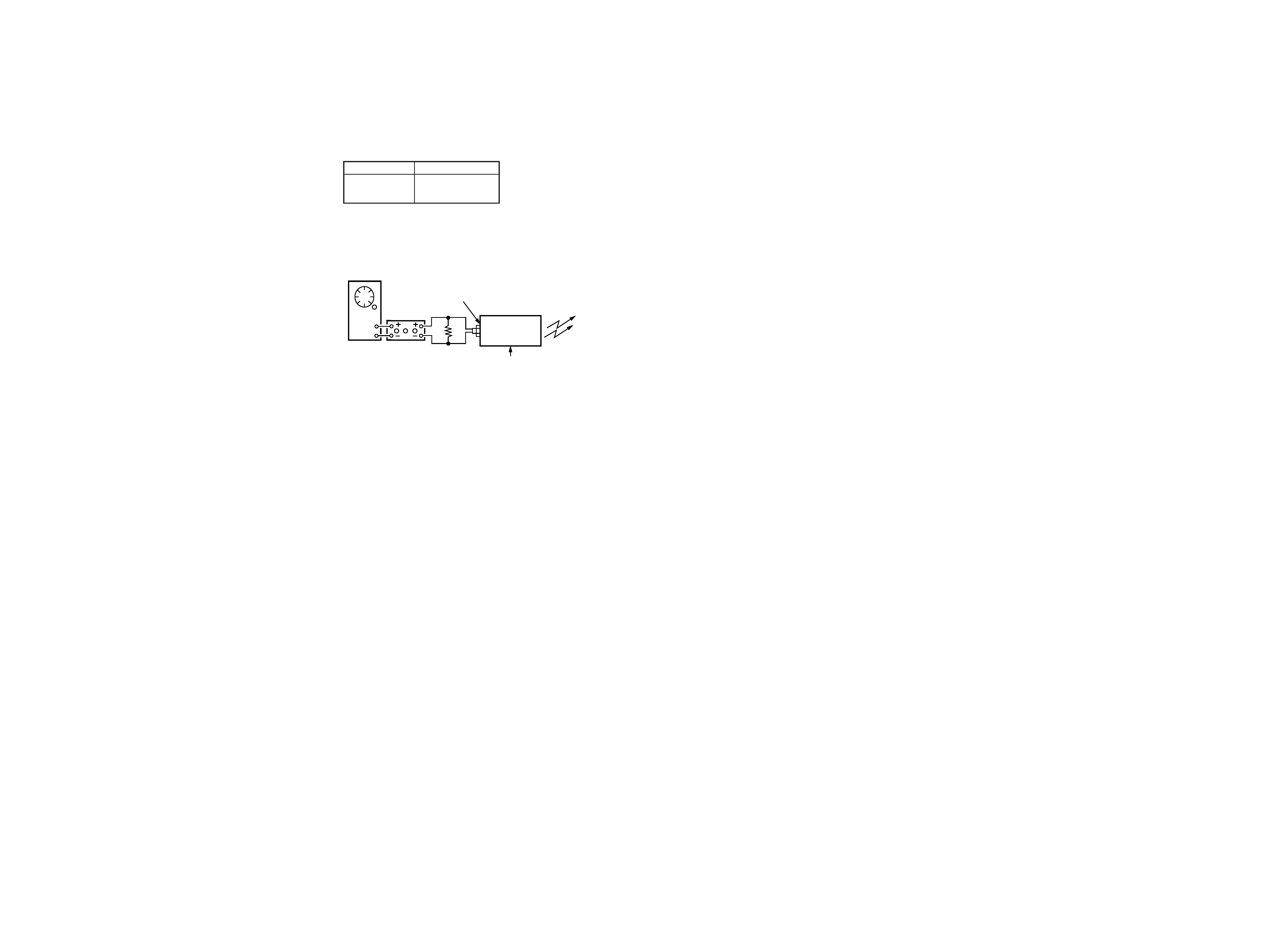
Connection points and Adjustment Location :
RXboard(Seepage5)
Note :
1. Usetransmitterwithcheckandadjustmentalreadycompleted.
2. Thetransmittersectionadjustmentsshouldbecompletedbefore
performingtheheadphonessectionadjustment.
3. Onadjustingtheheadphonessection,usethetransmitterasa
jig.
Headphones
Transmitter
MDR-RF430
TMR-RF450R
MDR-RF450
Setting :
Transmitter
J404
power supply
(DC 11V)
L-CH (J403)
1kHz 316mVrms (7.8dB)
AF OSC
ATT
Jig
600
Connection points and Adjustment Location :
RXboard(Seepage5)
1. Feedasignaltojig(transmitter)andconnectapowersupplyto
DC IN 9V jack (J404).
5
6
Connectionpoints:
Adjustment Location :
RV302
Tuning Knob
RV301
VOL Knob
L301 : Receive Frequency Adjustment
RV303 : Separation Adjustment
[RX BOARD] (Component side)
[ RX BOARD ] (Conductor side)
oscilloscope
digital voltmeter
(AC range)
oscilloscope
digital voltmeter
(DC range)
r
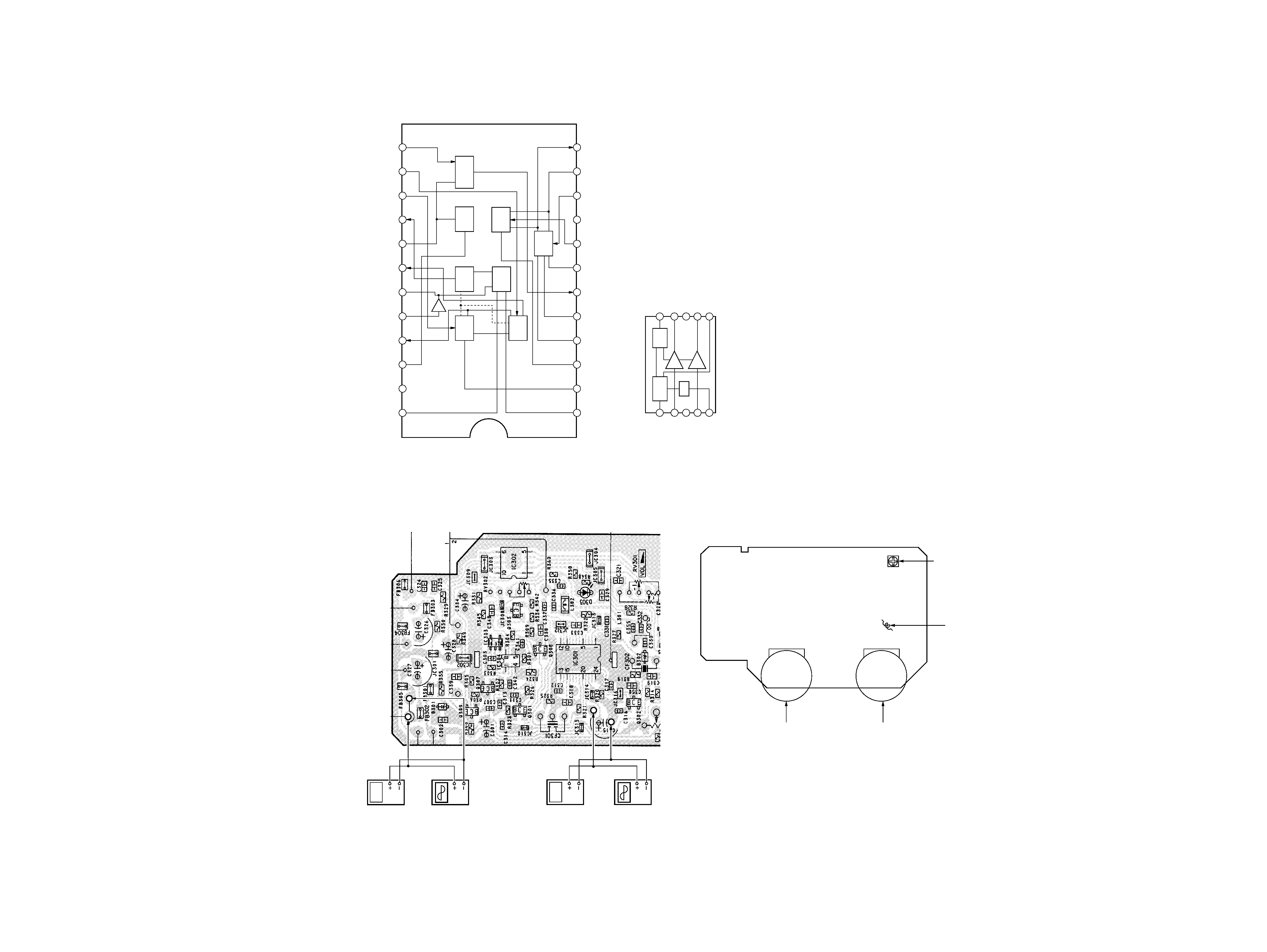
IC BLOCK DIAGRAMS
IC301 CXA1611N-T4
IC302 LA4533M
24
23
22
21
20
19
18
17
16
15
14
13
1
2
3
4
5
6
7
8
9
10
11
12
REGULATOR
AM·FE
FM·FE
RIPPLE
FILTER
TUNING
METER
DETUNE
DET
FM·IF
DISCRI
AM·IF
DET·AGC
DETUNE
DET
CONTROL
VCC
RIPPLE
FILTER
DET
OUT
AFC
AGC
AFC
AGC
AM
IF
OUT
GND
METER
FM
IF
IN
AM
IF
IN
FM/AM
BAND
SELECT
DETUNE
DET
GND
FM
DISCRI
AM
OSC
AFC
FM
OSC
REG
OUT
FM
RF
AM
RF
IN
NC
FM
RF
IN
GND
FM/AM
FE
OUT
POWER
SWITCH
MUTE
CIRCIUT
BIAS
1
2
3
4
5
6
7
8
9
10 MT/SW
OUT1
POWER GND
OUT2
VCC
P/SW
IN1
PRE GND
IN2
REF
AMP2
AMP1
SECTION 3
DIAGRAMS