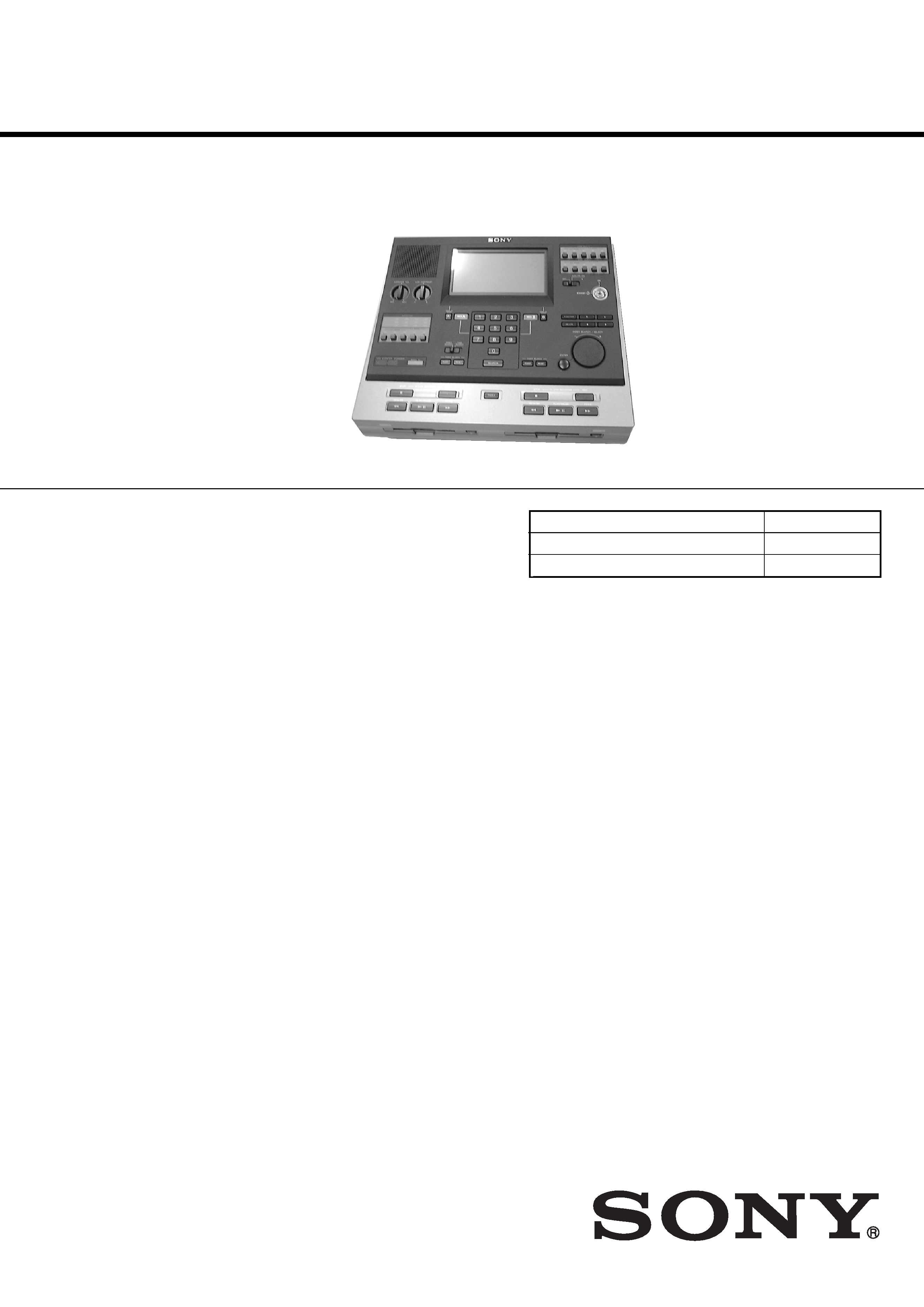
MDCC-2000
US Model
SERVICE MANUAL
MD CONFER-CORDER
Sony Corporation
Personal Audio Company
Shinagawa Tec Service Manual Production Group
9-873-111-12
2001G1600-1
© 2001.7
SPECIFICATIONS
Ver 1.1 2001. 07
US and foreign patents licensed from Dolby
Laboratories Licensing Corporation
Laser diode properties
Material: GaAlAs
Wavelength: 780 nm
Emission duration: Continuous
Laser output: Less than 44.6
µW
(This output is the value measured at a distance of
about 200 mm from the lens surface on the optical
pick-up block with 7 mm aperture.)
Revolutions
400 rpm to 1800 rpm (CLV)
Error correction
Advanced Cross Interleave Reed Solomon Code (ACIRC)
Sampling frequency
44.1 kHz
Coding
ATRAC 3 (Adaptive TRansform Acoustic Coding 3)
Modulation system
EFM (Eight to Fourteen Modulation)
Number of channels
2 or 4 monaural channels
Frequency response
5010,000 Hz
Speaker
Approx. 5.0 cm (2 inches) dia.
Power output
600 mW (at 10% distortion)
Input
MIC: Canon XLR-3-31 type 0.44 mV (-65 dB)
LINE IN 1-4: mini jack 0.49 V (-4 dB)
Output
EAR (minijack)
for 8300
earphones
LINE OUT 1,2 (minijack) 0.22 V (-11 dB) load inpedance 47 k
ADA (minijack) 0.22 V (-11 dB) load inpedance 10 k
PA (minijack) 0.22 V (-11 dB) load inpedance 47 k
PC (9 pin D-sub)
DISPLAY (modular)
Other connector
CONTROL UNIT connector
REMOTE jack
Power requirements
12 V DC
DC IN 12V jack accepts the supplied AC power
adaptor for use on 120 V AC, 60 Hz
Dimensions
Approx. 320 x 280 x 118 mm (w/h/d)
(125/8 x 111/8 x 43/4 inches)
including projecting parts and controls
Mass
Approx. 4.5 kg (9 lb 15 oz)
Accessories supplied
AC power adaptor (1)
AC power cord (1)
Sony CR2032 lithium battery (1)
MiniDisc (2)
Design and specifications are subject to change without notice.
Model Name Using Similar Mechanism
NEW
MD Mechanism Type
CCMD-2000
Optical Pick-up Mechanism Type
KMS-250A

2
MDCC-2000
1. GENERAL ·································································· 3
2. DISASSEMBLY
2-1.
Cabinet (Upper) Section ··············································· 6
2-2.
Switch Section ······························································ 7
2-3.
LCD Section ································································· 7
2-4.
I/O Section ··································································· 8
2-5.
Volume Section ···························································· 8
2-6.
Main Board ·································································· 9
2-7.
Connector Section ························································ 9
2-8.
Door ··········································································· 10
2-9.
MD Board ·································································· 10
2-10. Base Unit Section ······················································· 11
2-11. BUM-F1 Board ·························································· 11
2-12. REC/PB Head Assy (HR901) Section ······················· 12
2-13. Holder Assy, Cartridge Section ·································· 12
2-14. Holder Assy, Cartridge Installation ···························· 13
2-15. Optical Pick-up (KMS-250A) Section ······················· 13
3. TEST MODE ···························································· 14
4. ELECTRICAL ADJUSTMENTS ··························· 27
5. DIAGRAMS
5-1.
Circuit Boards Location ············································· 29
5-2.
Block Diagrams MD Section ···································· 30
I/O Section ································································· 31
FIFO Section ······························································ 32
CPU Section ······························································· 33
LCD Section ······························································· 34
5-3.
Printed Wiring Board MD Section ···························· 35
5-4.
Schematic Diagram MD Section (1/4) ······················ 36
5-5.
Schematic Diagram MD Section (2/4) ······················ 37
5-6.
Schematic Diagram MD Section (3/4) ······················ 38
5-7.
Schematic Diagram MD Section (4/4) ······················ 39
5-8.
Schematic Diagram BUM Section ···························· 40
5-9.
Printed Wiring Board BUM Section ························· 41
5-10. Schematic Diagram Main Section (1/12) ·················· 42
5-11. Schematic Diagram Main Section (2/12) ·················· 43
5-12. Schematic Diagram Main Section (3/12) ·················· 44
5-13. Schematic Diagram Main Section (4/12) ·················· 45
5-14. Schematic Diagram Main Section (5/12) ·················· 46
TABLE OF CONTENTS
5-15. Schematic Diagram Main Section (6/12) ·················· 47
5-16. Schematic Diagram Main Section (7/12) ·················· 48
5-17. Schematic Diagram Main Section (8/12) ·················· 49
5-18. Schematic Diagram Main Section (9/12) ·················· 50
5-19. Schematic Diagram Main Section (10/12) ················ 51
5-20. Schematic Diagram Main Section (11/12) ················ 52
5-21. Schematic Diagram Main Section (12/12) ················ 53
5-22. Printed Wiring Board Main Section ·························· 54
Main Section (1/4) ····················································· 55
Main Section (2/4) ····················································· 56
Main Section (3/4) ····················································· 57
Main Section (4/4) ····················································· 58
5-23. Printed Wiring Board Mute Section ·························· 59
5-24. Schematic Diagram AUDIO Section ························· 60
5-25. Printed Wiring Board Audio Section ························· 61
5-26. Schematic Diagram Level Meter Section ·················· 62
5-27. Printed Wiring Board Level Meter Section ··············· 63
5-28. Schematic Diagram LCD Section ····························· 64
5-29. Printed Wiring Board LCD Section ·························· 65
5-30. Schematic Diagram Switch Section ·························· 66
5-31. Printed Wiring Board Switch Section ······················· 67
5-32. Schematic Diagram Foot Switch Section ·················· 68
5-33. Printed Wiring Board Foot Switch Section ··············· 69
5-34. Schematic Diagram Volume/Serial I/O Section ········ 70
5-35. Printed Wiring Board Volume/Serial I/O Section ····· 71
5-36. Schematic Diagram Line Selector Section ················ 72
5-37. Printed Wiring Board Line Selector Section ············· 73
5-38. IC Pin Function Description ······································ 74
5-39. IC Block Diagrams ····················································· 77
6. EXPLODED VIEWS
6-1.
Cabinet Section ·························································· 85
6-2.
Key Section ································································ 86
6-3.
LCD Section ······························································· 87
6-4.
Connector Section ······················································ 88
6-5.
MD Mechanism Section
(CCMD-2000) (Deck-A/Deck-B) ······························ 89
7. ELECTRICAL PARTS LIST ·································· 90
SAFETY-RELATED COMPONENT WARNING!!
COMPONENTS IDENTIFIED BY MARK
! OR DOTTED LINEWITH
MARK
!ON THE SCHEMATIC DIAGRAMS AND IN THE PARTS
LIST ARE CRITICAL TO SAFE OPERATION.
REPLACE THESE COMPONENTS WITH SONY PARTS WHOSE
PART NUMBERS APPEAR AS SHOWN IN THIS MANUAL OR IN
SUPPLEMENTS PUBLISHED BY SONY.
Flexible Circuit Board Repairing
· Keep the temperature of the soldering iron around 270
°C during
repairing.
· Do not touch the soldering iron on the same conductor of the
circuit board (within 3 times).
· Be careful not to apply force on the conductor when soldering or
unsoldering.
Notes on chip component replacement
· Never reuse a disconnected chip component.
· Notice that the minus side of a tantalum capacitor may be dam-
aged by heat.
3
MDCC-2000
CAUTION
Use of controls or adjustments or performance of
procedures other than those specified herein may result in
hazardous radiation exposure.
NOTES ON HANDLING THE OPTICAL PICK-UP
BLOCK OR BASE UNIT
The laser diode in the optical pick-up block may suffer electrostatic
break-down because of the potential difference generated by the
charged electrostatic load, etc. on clothing and the human body.
During repair, pay attention to electrostatic break-down and also
use the procedure in the printed matter which is included in the
repair parts.
The flexible board is easily damaged and should be handled with
care.
NOTES ON LASER DIODE EMISSION CHECK
Never look into the laser diode emission from right above when
checking it for adjustment. It is feared that you will lose your sight.
Unleaded solder
Boards requiring use of unleaded solder are printed with the lead-
free mark (LF) indicating the solder contains no lead.
(Caution: Some printed circuit boards may not come printed with
the lead free mark due to their particular size.)
: LEAD FREE MARK
Unleaded solder has the following characteristics.
· Unleaded solder melts at a temperature about 40°C higher than
ordinary solder.
Ordinary soldering irons can be used but the iron tip has to be
applied to the solder joint for a slightly longer time.
Soldering irons using a temperature regulator should be set to
about 350°C.
Caution: The printed pattern (copper foil) may peel away if the
heated tip is applied for too long, so be careful!
· Strong viscosity
Unleaded solder is more viscous (sticky, less prone to flow) than
ordinary solder so use caution not to let solder bridges occur such
as on IC pins, etc.
· Usable with ordinary solder
It is best to use only unleaded solder but unleaded solder may
also be added to ordinary solder.
4
MDCC-2000
SECTION 1
GENERAL
4 Introduction
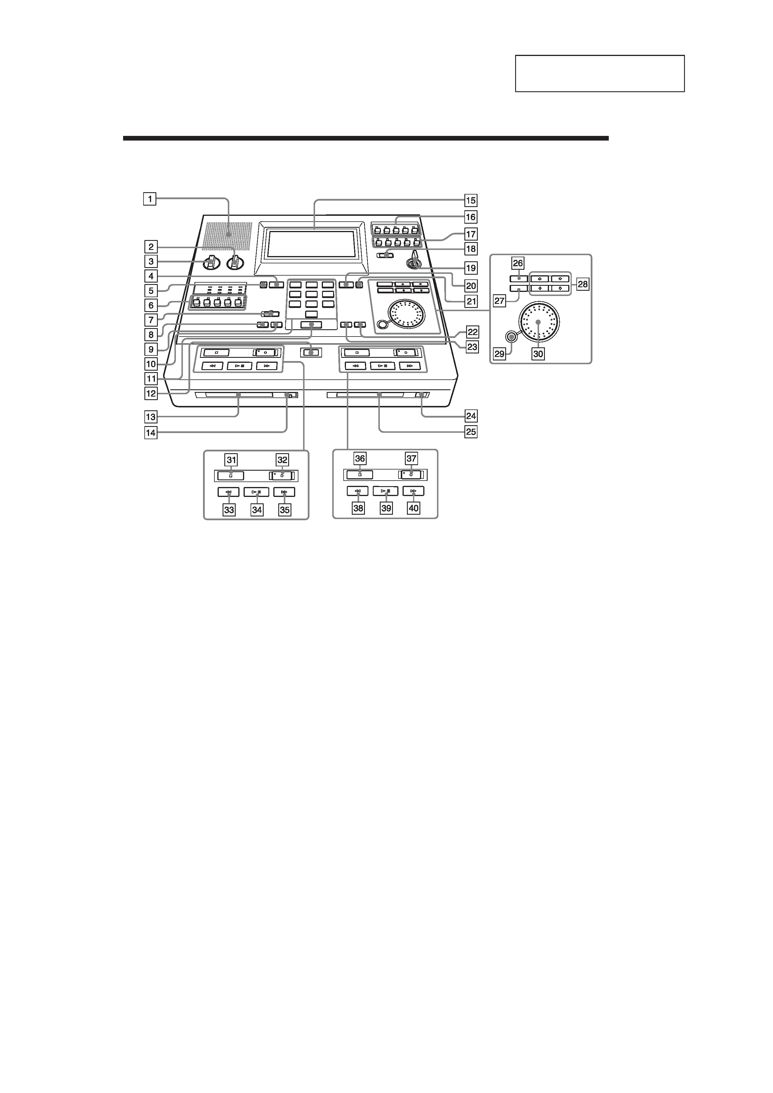
Location and Function of Controls
For details, refer to the pages indicated in ( ).
1
Built-in speaker
2
LCD CONTRAST control
Adjusts the contrast of the display.
3
MONITOR VOL control
4
DECK A button (17, 18)
5
DISPLAY MODE A button (21)
6
MONITOR select buttons (ALL/1/2/3/4)
7
SEARCH selector (17, 18)
(INDEX SEARCH/TIME SEARCH)
8
POINT SEARCH·POINT button (deck A) (20)
9
POINT SEARCH·RESET button (deck A) (20)
q;
Number buttons
qa
SEARCH button (17, 18)
qs
INDEX button (14)
qd
MD insertion slot (deck A)
qf
Z EJECT button (deck A)
qg
LCD display
qh
LINE OUT 1 select buttons (ALL/1/2/3/4) (31)
qj
LINE OUT 2 select buttons (ALL/1/2/3/4) (31)
qk
PA/ADA selector (OFF/ON [ADA/PA]) (30)
Switches the output to the PA/ADA jacks on
or off.
ql
STANDBY switch
w;
DECK B button (17, 18)
wa
DISPLAY MODE B button (21)
ws
POINT SEARCH·RESET button (deck B) (20)
wd
POINT SEARCH·POINT button (deck B) (20)
wf
Z EJECT button (deck B)
wg
MD insertion slot (deck B)
wh
FUNCTION button
wj
DELETE button
wk
Arrow buttons
wl
ENTER button
e;
Jog dial
ea
x STOP button (deck A)
es
z REC button (deck A)
ed
m REW/BS button (deck A)
ef
u PLAY/PAUSE button (deck A)
eg
M FF/FS button (deck A)
eh
x STOP button (deck B)
ej
z REC button (deck B)
ek
m REW/BS button (deck B)
el
u PLAY/PAUSE button (deck B)
r;
M FF/FS button (deck B)
This section is extracted from
instruction manual.
5
MDCC-2000
6 Introduction
1
A: display (deck A)
Indicates the disc inserted in deck A or the
status of deck A as follows:
BLANK: a blank disc
NO DISC: no disc
PB ONLY: a commercially available recorded
disc (for playback only)
PROTECTED: a protected disc (3)
RECORDED: a recorded disc
2
TIME display (deck A)
Indicates the recorded time at the current
location for each index item. It blinks during
time search. (18)
3
(copied) display (deck A)
Indicates that a disc digitally copied with the
Copy function is inserted. (26)
4
INDEX counter (deck A)
Lights up when a disc is inserted.
Blinks during an index search. (17)
5
END display (deck A)
This shows the end of the disc.
6
Disc status display (deck A)
Indicates the status of the disc with pictures.
7
DECK A/DECK B display
Indicates various data by characters and various
error messages. (38)
8
Disc position display
Indicates the current playback/recording location
on the disc by a white box. Already recorded
parts are indicated in black. The further it is to
the right, the closer the disc is to the end.
Depending on the condition of the disc, the black
part might not reach the far right even if the disc
is full.
9
DATE/TIME display
Indicates the current date and time.
0
B: display (deck B)
Indicates the same contents as deck A.
qa
TIME display (deck B)
qs
(copied) display (deck B)
qd
Disc status display (deck B)
qf
END display (deck B)
qg
INDEX counter (deck B)
qh
REC MODE display
Indicates the recording mode (2ch/4ch) currently
selected.
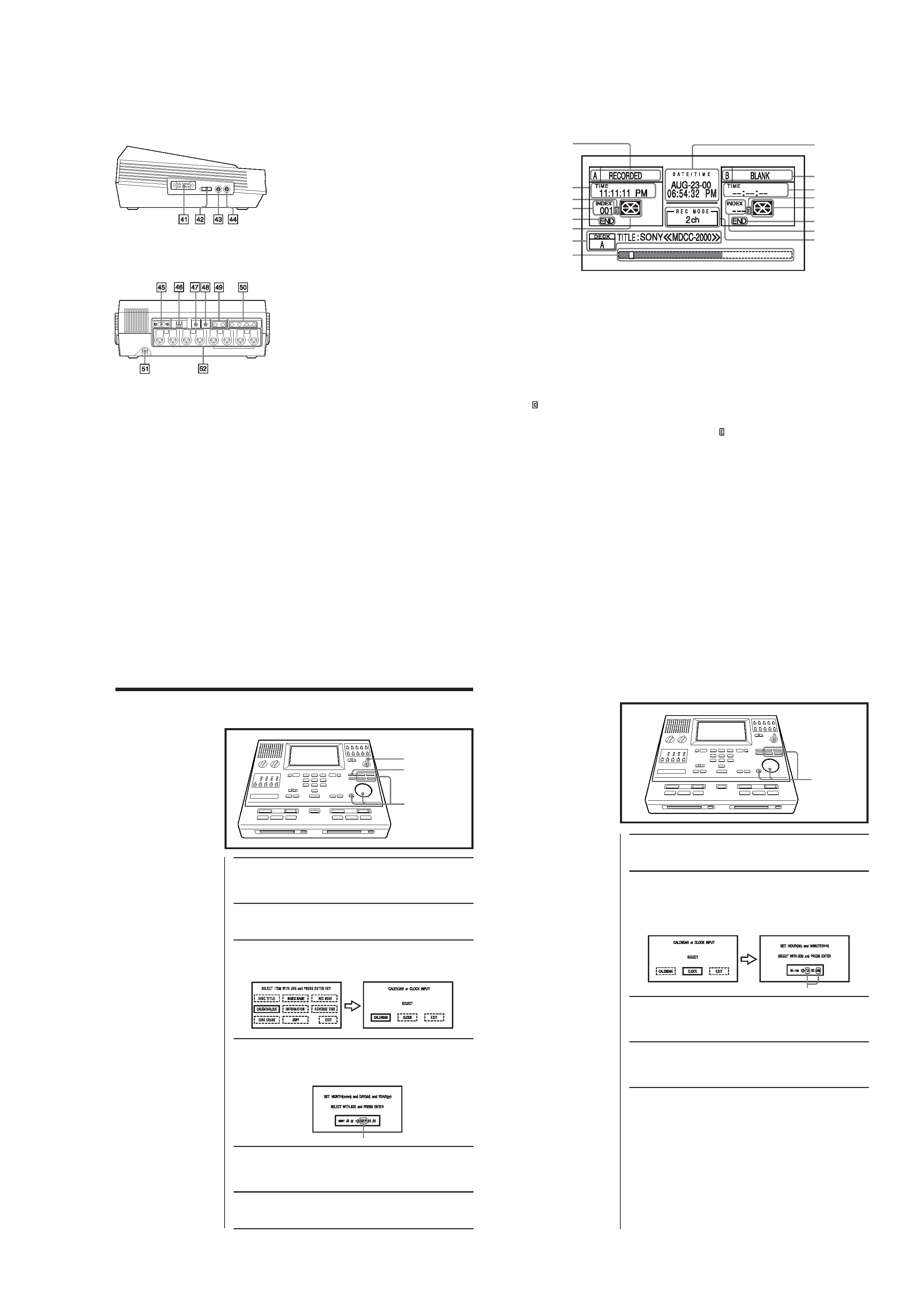
Display Window (Information screen)
1
2
3
4
5
6
7
8
9
0
qa
qs
qd
qf
qg
qh
8 Setting Up
Setting the Date and Time
1 Insert the key and set it to ON.
You will see the initial screen in a few seconds.
2 Press FUNCTION.
3 Select CALENDAR,CLK using the jog dial or the arrow
buttons, and press ENTER.
You will see the CALENDAR or CLOCK INPUT screen.
4 Select CALENDAR using the jog dial or the arrow buttons,
and press ENTER.
You will see the SET MONTH (mmm) and DAY (dd) and YEAR (yy)
screen with the name of a month blinking.
5 Set the month using the jog dial or J/j buttons, and
press ENTER.
You will see "01" of the day blinking.
6 Set the day and the year in the same way as step 5.
When the year is set, the display will return to the information screen.
1
2
3, 4, 5, 6
Setting the Date
blink
To record the date and time
etc. on MiniDiscs when you
record, be sure to set the Date
and Time.
Note
You cannot use the K/k buttons
when setting the month, day and
year.
9
Setting Up
1 Carry out steps 2 and 3 of "Setting the Date".
You will see the CALENDER or CLOCK INPUT screen.
2 Select CLOCK using the jog dial or the arrow buttons, and
press ENTER.
You will see the SET HOUR (hh) and MINUTE (mm) screen with the
hours and AM/PM blinking.
3 Set the hour using the jog dial or J/j buttons, and press
ENTER.
You will see the minutes blinking.
4 Set the minutes in the same way as step 3.
The display will return to the information screen and the clock will
start.
blink
Note
You cannot use the K/k buttons
when setting the hour and minute.
Setting the Time
2, 3, 4
5
Introduction
Left side
Rear
ra
CONTROL UNIT connector (32)
rs
TRANSCRIBE selector (33)
rd
REMOTE jack (15)
rf
EAR jack (16)
rg
PC connector (RS-232C type)
rh
DISPLAY connector
Used for connection of an external
counter unit.
rj
ADA jack
Allows the unit to be connected to a
separately purchased amplifier
system.
rk
PA (public address) jack (30)
rl
LINE OUT jacks
t;
LINE IN jacks
ta
DC IN 12V
ts
Microphone connectors
(Canon XLR-3-31 type)