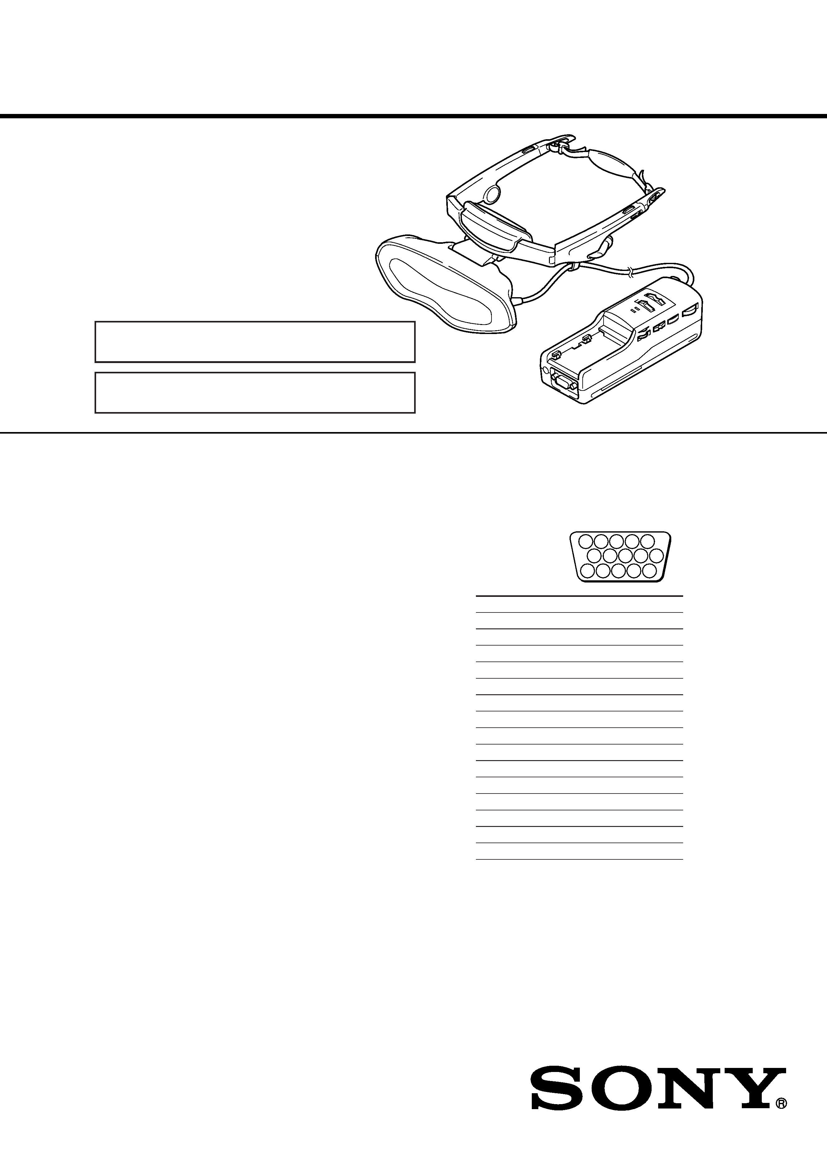
SERVICE MANUAL
SPECIFICATIONS
PERSONAL LCD DISPLAY
LDI-D100B
9-928-133-01
Continued on next page
NTSC Model
Power supply
AC power adapter: AC-PLM3
100-240 V AC, 50/60 Hz, 16 W
Output voltage 8.4 V, 1.6 A
Battery pack: NP-F550/F750/F950
(not supplied)
Power consumption
10 W (approx., PC mode)
12 W (approx., VIDEO mode)
Operating temperature
41
°F to 95°F (5°C to 35°C)
Storage temperature
14
°F to 140°F (10°C to 60°C)
Dimensions
Display unit:
Approx.5 7/8
× 1 15/16 × 3 1/2 inches
(Approx.149
× 48 × 86 mm)
(w/h/d folded)
Power supplybox:
Approx.2 1/4
× 1 7/8 × 6 3/8 inches
(Approx.54
× 47 × 160 mm)
(w/h/d)
not including projecting parts and
controls
Mass
Display unit: Approx.4.2 oz. (120 g)
Power supply box: Approx.9.2 oz. (260 g)
Video signal
NTSC color, CCIR standards
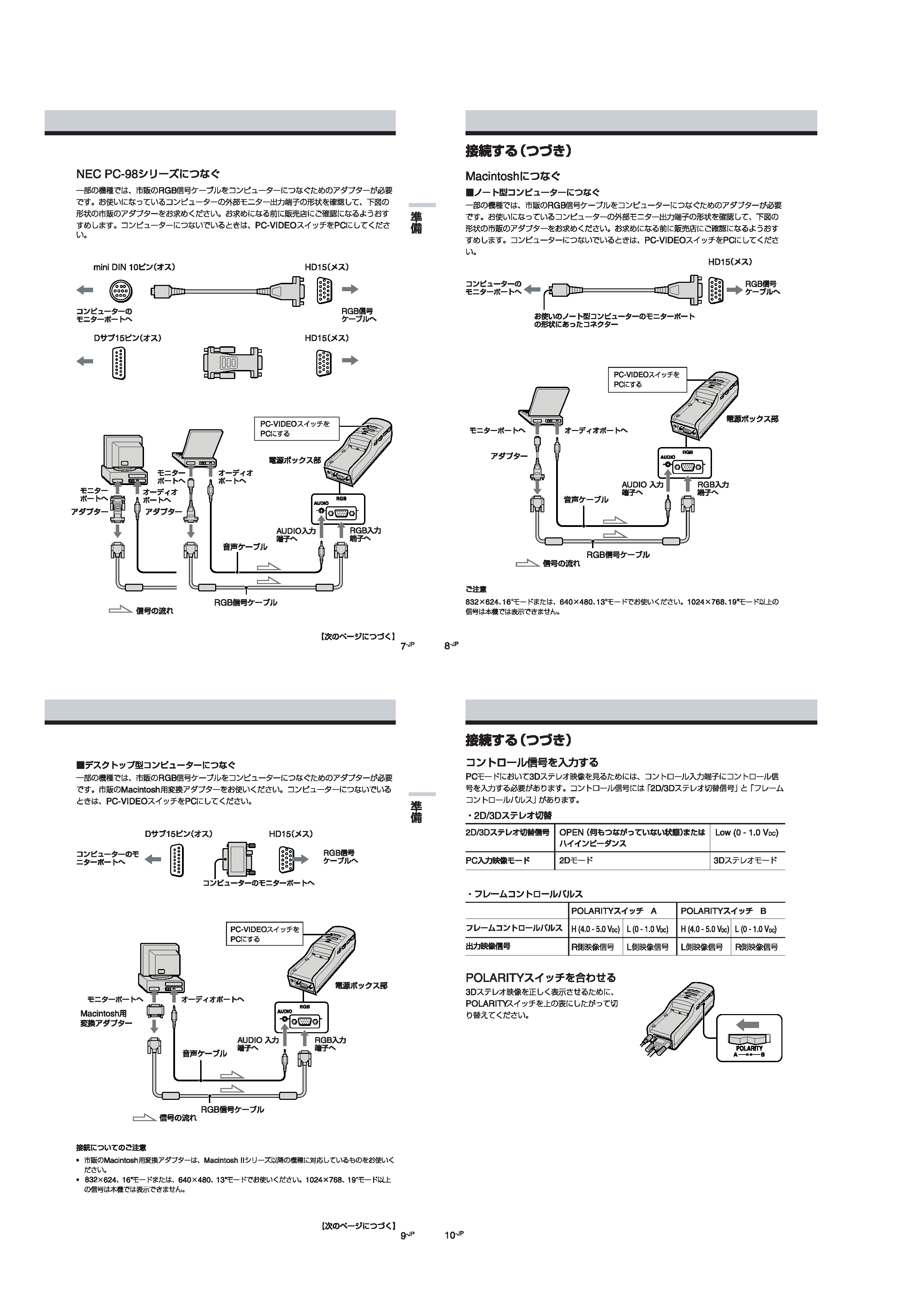
VIDEO Input
PC mode
RGB signal: HD15
Pin Assignment
5 4 3 2 1
8 7 6
15 14 13 12 11
10 9
Pin No.
Signal
1
R (Red)
2
G (Green)
3
B (Blue)
4
5
GND
6
R (Red) GND
7
G (Green) GND
8
B (Blue) GND
9
10
GND
11
GND
12
13
SYNC (Horizontal)
14
SYNC (Vertical)
15
"
"
NOTE : "SECTION 4 DIAGRAMS" is provided in the
separate manual (9-928-133-31).

2
0
·
·
·
·
·
Notes on chip component replacement
· Never reuse a disconnected chip component.
· Notice that the minus side of a tantalum capacitor may be dam-
aged by heat.
Flexible Circuit Board Repairing
· Keep the temperature of the soldering iron around 270 °C dur-
ing repairing.
· Do not touch the soldering iron on the same conductor of the
circuit board (within 3 times).
· Be careful not to apply force on
SAFETY-RELATED COMPONENT WARNING!!
COMPONENTS IDENTIFIED BY MARK 0 OR DOTTED
LINE WITH MARK 0 ON THE SCHEMATIC DIAGRAMS
AND IN THE PARTS LIST ARE CRITICAL TO SAFE
OPERATION. REPLACE THESE COMPONENTS WITH
SONY PARTS WHOSE PART NUMBERS APPEAR AS
SHOWN IN THIS MANUAL OR IN SUPPLEMENTS PUB-
LISHED BY SONY.
ATTENTION AU COMPOSANT AYANT RAPPORT
À LA SÉCURITÉ!
LES COMPOSANTS IDENTIFIÉS PAR UNE MARQUE 0
SUR LES DIAGRAMMES SCHÉMATIQUES ET LA LISTE
DES PIÈCES SONT CRITIQUES POUR LA SÉCURITÉ
DE FONCTIONNEMENT. NE REMPLACER CES COM-
POSANTS QUE PAR DES PIÈCES SONY DONT LES
NUMÉROS SONT DONNÉS DANS CE MANUEL OU
DANS LES SUPPLÉMENTS PUBLIÉS PAR SONY.
VIDEO mode
S VIDEO input:4-pin miniDIN
Y: 1 Vp-p, 75 ohms, unbalanced, sync
negative
C: 0.286 Vp-p, 75 ohms, unbalanced,
sync negative
AUDIO input
Stereo miniplug
CONTROL input connector
(used in PC
mode only)
Special type stereo miniplug
Screen resolution
Horizontal:832 dots (max.)
Vertical: 624 lines (max.)
Supplied accessory
AC power adapter: AC-PLM3 (1)
Power cords (2)
Design and specifications are subject to
change without notice.

3
1.
GENERAL
1-1
1-1
1-1
1-1
1-4
1-4
1-5
1-5
1-7
1-7
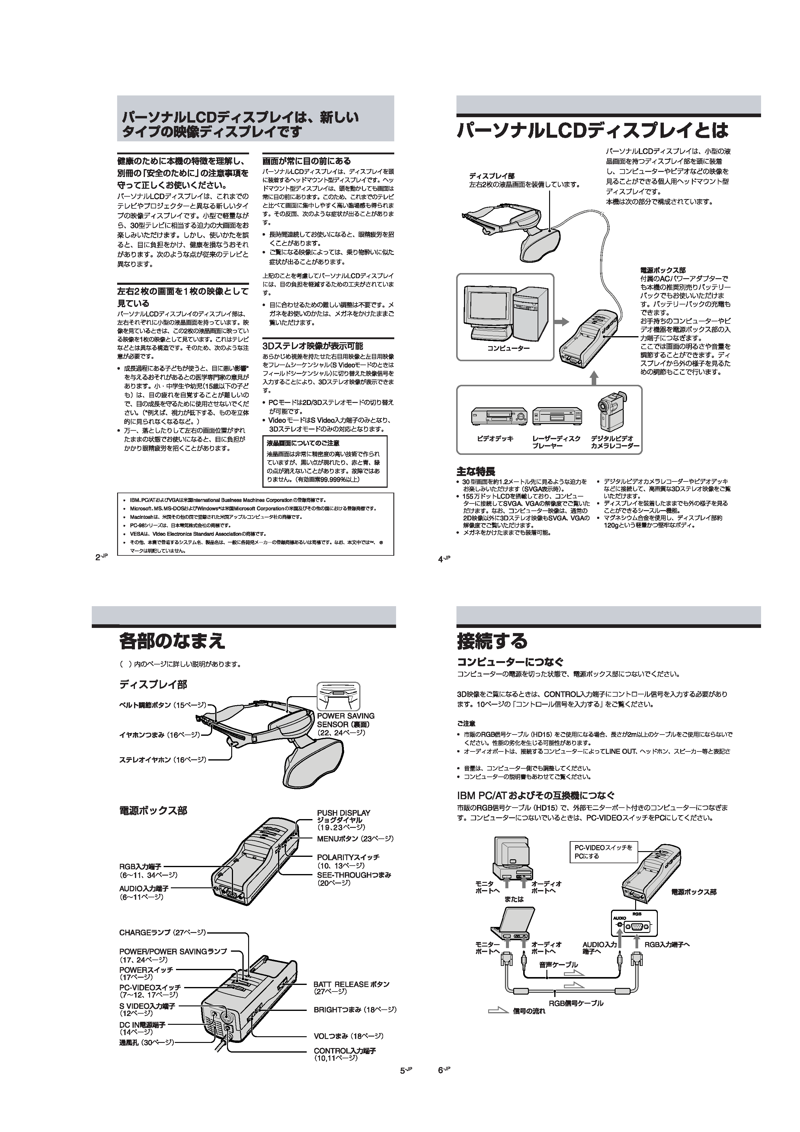
The Personal LCD Display is
a Brand-new Concept in Visual Display ..................... 1-8
About the Personal LCD Display ................................ 1-8
Locating the Parts and Controls .................................. 1-8
Connecting the Personal LCD Display ....................... 1-9
Wearing the Personal LCD Display ............................ 1-11
Using the Personal LCD Display ................................ 1-11
Viewing the Surrounding Environment ...................... 1-12
Adjusting the Sound and Picture ................................. 1-12
Using the Optional Battery Pack ................................. 1-14
Precautions ................................................................... 1-14
2.
DISASSEMBLY ...................................................... 2-1
3.
.................................................................... 3-1
ELECTRICAL ADJUSTMENTS ...................... 3-16
4.
DIAGRAMS (Separete Volume: 9-928-133-31)
4-1.
Block Diagram AUDIO/VIDEO Section ............. 4-1
4-2.
Block Diagram
A/D, D/A, OSD, SYNC Section ............................ 4-5
4-3.
Block Diagram
GAMMA CONTROL/LCD DRIVE Section ........ 4-7
4-4.
Block Diagram
MODE CONTROL/SENSOR/LCS Section ......... 4-9
4-5.
Block Diagram POWER SUPPLY Section ......... 4-11
Note for Printed Wiring Boards and
Schematic Diagrams .................................................... 4-14
4-7.
Printed Wiring Board JK-136 (H) Board ............. 4-15
4-8.
Schematic Diagram JK-136 (H) Board ................. 4-16
4-9.
Schematic Diagram YC-148 (H) Board (1/3) ....... 4-17
4-10. Schematic Diagram YC-148 (H) Board (2/3) ....... 4-19
4-11. Schematic Diagram YC-148 (H) Board (3/3) ....... 4-24
4-12. Printed Wiring Board YC-148 (H) Board ............ 4-27
4-13. Printed Wiring Board MA-324 (H) Board ........... 4-30
4-14. Schematic Diagram MA-324 (H) Board (1/7) ...... 4-33
4-15. Schematic Diagram MA-324 (H) Board (2/7) ...... 4-37
4-16. Schematic Diagram MA-324 (H) Board (3/7) ...... 4-41
4-17. Schematic Diagram MA-324 (H) Board (4/7) ...... 4-44
4-18. Schematic Diagram MA-324 (H) Board (5/7) ...... 4-47
4-19. Schematic Diagram MA-324 (H) Board (6/7) ...... 4-51
4-20. Schematic Diagram MA-324 (H) Board (7/7) ...... 4-53
4-21. Printed Wiring Board LC-61 (F) Board ............... 4-55
4-22. Schematic Diagram LC-61 (F) Board ................... 4-57
4-23. Printed Wiring Board SW-306 (H) Board ........... 4-60
4-24. Schematic Diagram SW-306 (H) Board ............... 4-63
4-25. Printed Wiring Board DD-107 (H) Board ............ 4-65
4-26. Schematic Diagram DD-107 (H) Board ................ 4-67
5.
IC DIAGRAMS
5-1.
IC Block Diagrams ...................................................... 5-1
5-2.
IC Pin Function Description ........................................ 5-11
6.
EXPLODED VIEWS ............................................. 6-1
7.
ELECTRICAL PARTS LIST ............................ 7-1
TABLE OF CONTENTS
1-1
1-2