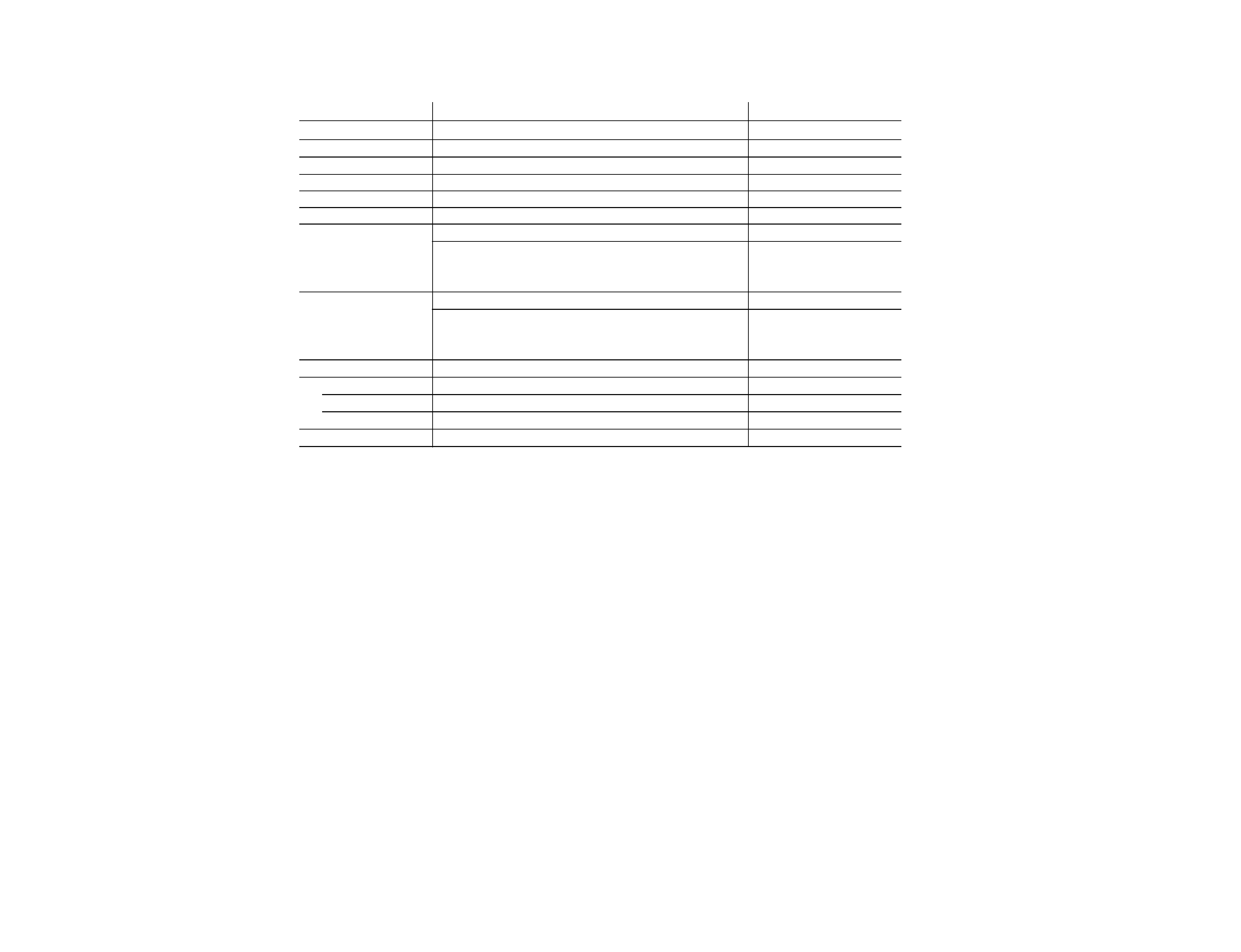
MODEL
COMMANDER DEST.
CHASSIS NO.
KV-G14DK2 RM-869
ME
SCC-U07R-A
KV-G14P2
RM-869
E
SCC-U03E-A
KV-G14P2S
RM-869
GE
SCC-U05H-A
KV-G14P2S
RM-869
Indonesia SCC-U10B-A
KV-G14Q2
RM-869
E
SCC-U03F-A
KV-G14Q2S RM-869
GE
SCC-U05J-A
MODEL
COMMANDER DEST. CHASSIS NO.
CHASSIS
TRINITRON ® COLOR TV
SERVICE MANUAL
BG-2S
2
KV-G14DK2/G14P2/G14P2S
KV-G14Q2/G14Q2S
RM-869
Note
Power requirements
110-240 V AC, 50/60 Hz
Power consumption (W) Indicated on the rear of the TV
Television system
B/G
Color system
PAL, PAL 60, NTSC4.43, NTSC3.58 (AV IN)
Channel coverage
VHF: E2 to E12 / UHF: E21 to E69 / CATV: S01 to S03, S1 to S41
Audio output (speaker)
3W
Inputs
(antenna): 75 ohms external terminal
... (video input) jacks: phono jacks
D (video): 1 Vp-p, 75 ohms
(audio): 500 mVrms, high impedance
Outputs
A (earphone) jack: minijack
Ú (monitor output) jacks: phono jacks
D (video): 1 Vp-p, 75 ohms
(audio): 500 mVrms
Picture tube
14 in.
Tube size (cm)
36.8
Measured diagonally
Screen size (cm)
33.7
Measured diagonally
Dimensions (w/h/d, mm) 373
× 346 × 412
Mass (kg)
11
SPECIFICATIONS
CAUTION
SHORT CIRCUIT THE ANODE OF THE PICTURE TUBE AND
THE ANODE CAP TO THE METAL CHASSIS, CRT SHIELD, OR
CARBON PAINTED ON THE CRT, AFTER REMOVING THE
ANODE.
SAFETY-RELATED COMPONENT WARNING!!
COMPONENTS IDENTIFIED BY SHADING AND MARK
! ON
THE SCHEMATIC DIAGRAMS, EXPLODED VIEWS AND IN THE
PARTS LIST ARE CRITICAL TO SAFE OPERATION. REPLACE
THESE COMPONENTS WITH SONY PARTS WHOSE PART
NUMBERS APPEAR AS SHOWN IN THIS MANUAL OR IN
SUPPLEMENTS PUBLISHED BY SONY.
Design and specifications are subject to change without notice.

3
KV-G14DK2/G14P2/G14P2S
KV-G14Q2/G14Q2S
RM-869
TABLE OF CONTENTS
SELF DIAGNOSIS FUNCTION ..................................
4
1. GENERAL ....................................................................
5
2. DISASSEMBLY
2-1.
Rear Cover Removal ............................................
10
2-2.
A Board Removal ................................................
10
2-3.
F1 Board Removal ...............................................
10
2-4.
Service Position ...................................................
10
2-5.
Replacement of Parts ...........................................
11
2-6.
Terminal Board Bracket Removal .......................
11
2-7.
Demagnetization Coil Removal ..........................
11
2-8.
Picture Tube Removal ..........................................
12
3. SET-UP ADJUSTMENTS
3-1.
Beam Landing ......................................................
13
3-2.
Convergence .........................................................
14
3-3.
Focus Adjustment ................................................
15
3-4.
Remote Commander Adjustments .......................
16
3-5.
G2 (Screen) and White Balance Adjustments .....
16
4. CIRCUIT ADJUSTMENTS
4-1.
Adjustments with Commander ............................
17
4-2.
Adjustment Method .............................................
18
4-3.
A Board Adjustment after IC003 (Memory)
Replacement .........................................................
22
4-4.
Picture Distortion Adjustment .............................
22
5. DIAGRAMS
5-1.
Block Diagram ......................................................
25
5-2.
Circuit Boards Location .......................................
28
5-3.
Schematic Diagrams and Printed Wiring Boards
28
(1)
Schematic Diagram of A Board ...........................
33
(2)
Schematic Diagrams of C and F1 Boards ............
38
5-4.
Semiconductors .....................................................
43
6. EXPLODED VIEW
6-1.
Chassis ..................................................................
45
7. ELECTRICAL PARTS LIST ....................................
47
Section
Title
Page
Section
Title
Page
4
KV-G14DK2/G14P2/G14P2S
KV-G14Q2/G14Q2S
RM-869
If no acknowledgement is returned from a device which is turned "ON", the device has a problem.
In this case, one of the LED's responding to the problem device will flicker a defined number of times.
Flickering is operated by lighting the LED's for 60ss each time.
The flickering frequency responding to each failed device is shown below.
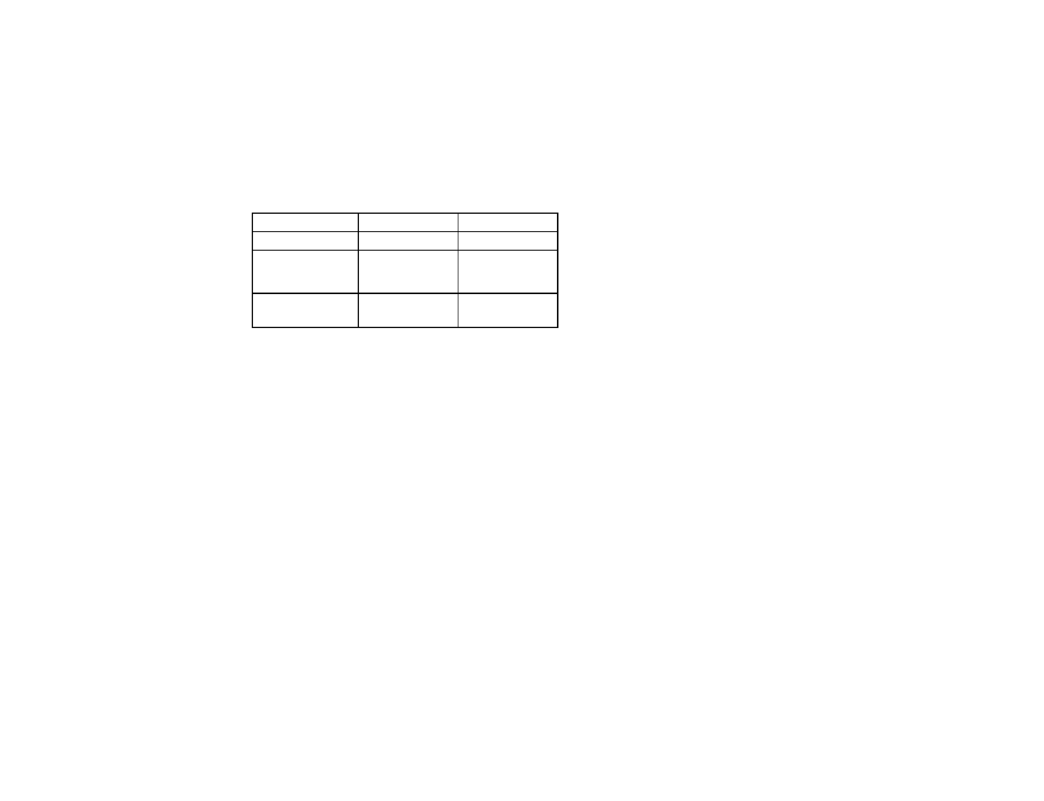
SELF DIAGNOSIS FUNCTION
Board name
Ref. No.
Device
Flickering Frequency
A Board
IC003
NONVOLATILE
MEMORY
(ST24C08FB6)
1
A Board
IC300
Y/C JUNGLE
(TDA8374A)
3
All the devices are checked one after another from the left of the table.
If an error is found, the responding LED will start flickering.
So, if more than 1 device have failed, only the one on the left side will flicker.
5
KV
-G14DK2/G14P2/G14P2S
KV
-G14Q2/G14Q2S
RM-869
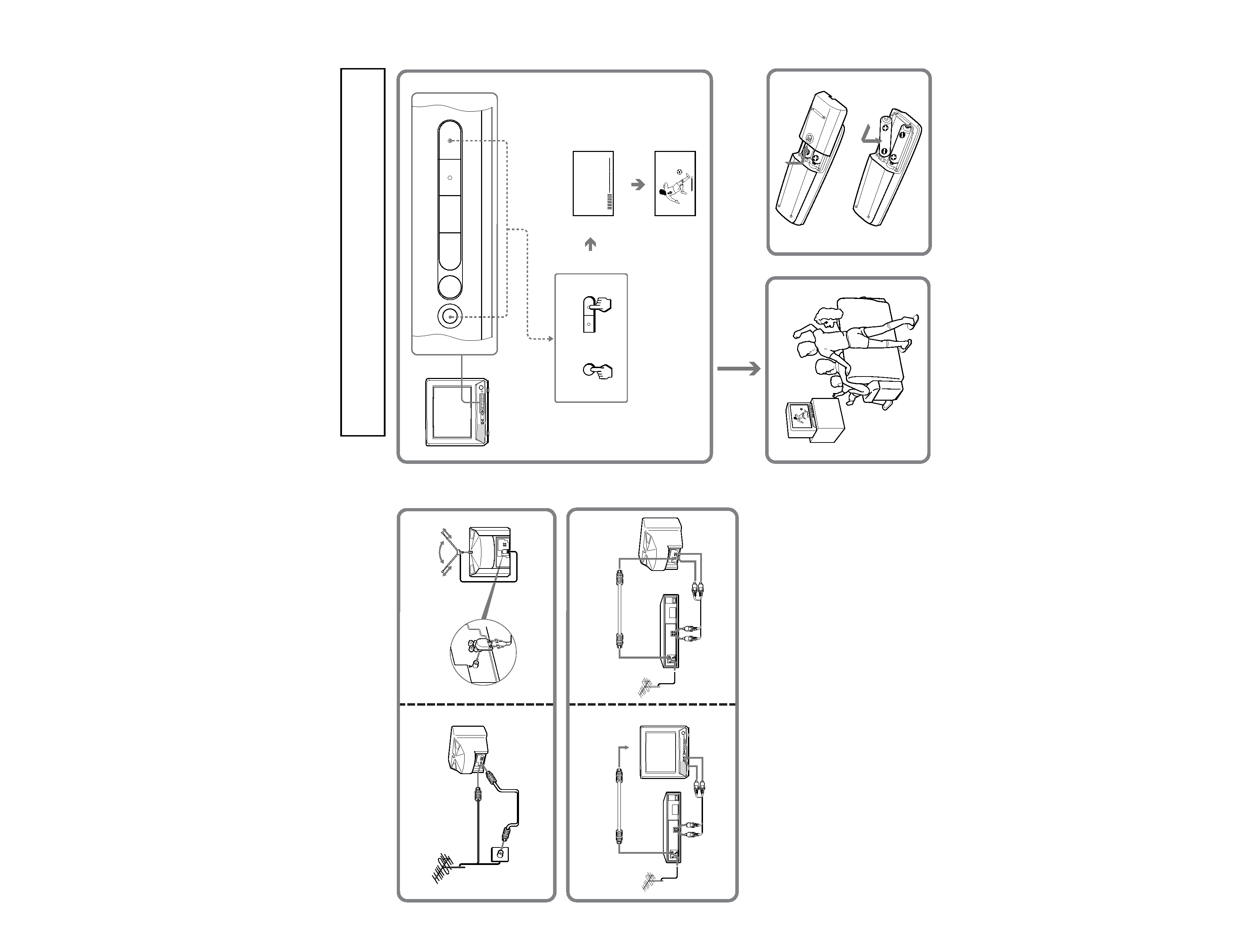
SECTION 1
GENERAL
The operating instructions mentioned here are partial abstracts from the
Operating Instructions Manual. The page numbers of the Operating
Instruction Manual remain as in this manual.
3
1
PROGR +
SELECT
PROGR +
VOLUME +
TV/VIDEO
SELECT
VHF
LOW
B/G
1
2
3
1
2