MODEL
COMMANDER DEST.
CHASSIS NO.
KV-EF34N90 RM-913
TAIWAN
SCC-P13EA
MODEL
COMMANDER DEST. CHASSIS NO.
CHASSIS
TRINITRON ® COLOR TV
SERVICE MANUAL
BG-3S
2
KV-EF34N90
RM-913
SPECIFICATIONS
Note
Power requirements
110 V AC, 50/60 Hz
Power consumption (W) Indicated on the rear of the TV
Television system
M
Color system
PAL, SECAM, NTSC4.43, NTSC3.58
Stereo/Bilingual system
B/G
MTS
B/G
Teletext Language
English, Chinese
Channel coverage
M
VHF: A2 to A13 / UHF: A14 to A69
CATV: A-6 to A-2, A to W+4, W+6 to W+29
(Antenna)
75-ohm external terminal
Audio output
15W + 15W
10% distortion
Number of terminal
D (Video)
Input: 4 Output: 1
Phono jacks; 1 VP-P, 75 ohms
(Audio)
Input: 4 Output: 1
Phono jacks; 500 mVrms
(S Video)
Input: 2
Y : 1 Vp-p, 75 ohms,
unbalanced, sync
negative
C : 0.286 Vp-p, 75 ohms
(Component Video) Input: 1
Phono jacks; Y : 1.0 Vp-p,
75 ohms, sync negative
CB : 0.7 Vp-p, 75 ohms
CR : 0.7 Vp-p, 75 ohms
Audio : 500 mVrms
2 (Headphone)
Output: 1
Stereo minijack
Picture tube
34 inch
Tube size (mm)
859 (Measured diagonally)
Screen size (mm)
800 (Measured diagonally)
Dimension (w/h/d, mm)
859
× 660.5 × 573.5
Mass (kg)
83
Design and specifications are subject to change without notice.
SAFETY-RELATED COMPONENT WARNING!!
COMPONENTS IDENTIFIED BY SHADING AND MARK ! ON
THE SCHEMATIC DIAGRAMS, EXPLODED VIEWS AND IN THE
PARTS LIST ARE CRITICAL TO SAFE OPERATION. REPLACE
THESE COMPONENTS WITH SONY PARTS WHOSE PART
NUMBERS APPEAR AS SHOWN IN THIS MANUAL OR IN
SUPPLEMENTS PUBLISHED BY SONY.
CAUTION
SHORT CIRCUIT THE ANODE OF THE PICTURE TUBE AND
THE ANODE CAP TO THE METAL CHASSIS, CRT SHIELD, OR
CARBON PAINTED ON THE CRT, AFTER REMOVING THE
ANODE.

3
KV-EF34N90
RM-913
TABLE OF CONTENTS
Section
Title
Page
SELF DIAGNOSIS FUNCTION ................................
4
1. GENERAL ........................................................................
8
2. DISASSEMBLY
2-1.
Rear Cover Removal ................................................ 28
2-2.
Speaker Box Removal ............................................. 28
2-3.
Chassis Assy Removal ............................................. 28
2-4.
Service Position ....................................................... 28
2-5.
D2 and DH Boards Removal ................................... 29
2-6.
J1 Board RF Splitter Removal ................................. 29
2-7.
P Boards Removal ................................................... 29
2-8.
A and B Boards Removal ........................................ 30
2-9.
H1 Board Removal .................................................. 30
2-10. Demagnetization Coil Removal .............................. 30
2-11. Top Switch Removal ................................................ 30
2-12. Picture Tube Removal .............................................. 31
3. SET-UP ADJUSTMENTS
3-1.
Beam Landing .......................................................... 32
3-2.
Convergence ............................................................. 33
3-3.
Focus Adjustment .................................................... 34
3-4.
Neck Assy Twist Adjustment ................................... 35
3-5.
G2 (Screen) and White Balance Adjustments ......... 37
3-6.
Frequency (Free Run) Adjustment .......................... 37
4. CIRCUIT ADJUSTMENTS
4-1.
Adjustments with Commander ................................ 51
4-2.
Adjustment Method ................................................. 51
4-3.
Picture Quality Adjustments .................................... 59
4-4.
A Board Adjustment After IC003 (Memory)
Replacement ............................................................. 60
4-5.
Picture Distortion Adjustment ................................. 61
Section
Title
Page
5. DIAGRAMS
5-1.
Block Diagram ......................................................... 51
5-2.
Frame Schematic Diagram ...................................... 59
5-3
Circuit Boards Location .......................................... 63
5-4.
Schematic Diagrams and Printed Wiring Boards ... 63
(1)
Schematic Diagram of A (1/2) Board ..................... 67
(2)
Schematic Diagram of A (2/2) Board ..................... 71
(3)
Schematic Diagram of B(1/2) Board ....................... 75
(4)
Schematic Diagrams of B(2/2) and F Boards ......... 78
(5)
Schematic Diagram P (1/3) Board ......................... 89
(6)
Schematic Diagram of P (2/3) Board ..................... 92
(7)
Schematic Diagrams of P (3/3), J1,B4 Boards ...... 95
(8)
Schematic Diagrams of C and H1 Boards ............. 99
(9)
Schematic Diagrams of VM2 and DH Boards ....... 106
(10) Schematic Diagram of D2 Board ........................... 111
5-5.
Semiconductors ....................................................... 113
6. EXPLODED VIEWS
6-1.
Picture Tube ............................................................ 116
6-2.
Chassis .................................................................... 117
7. ELECTRICAL PARTS LIST ..................................... 118
4
KV-EF34N90
RM-913
The units in this manual contain a self-diagnostic function. If an error occurs, the STANDBY/TIMER lamp will automatically
begin to flash.
The number of times the lamp flashes translates to a probable source of the problem. A definition of the STANDBY/TIMER
lamp flash indicators is listed in the instruction manual for the user's knowledge and reference. If an error symptom cannot
be reproduced, the remote commander can be used to review the failure occurrence data stored in memory to reveal past
problems and how often these problems occur.
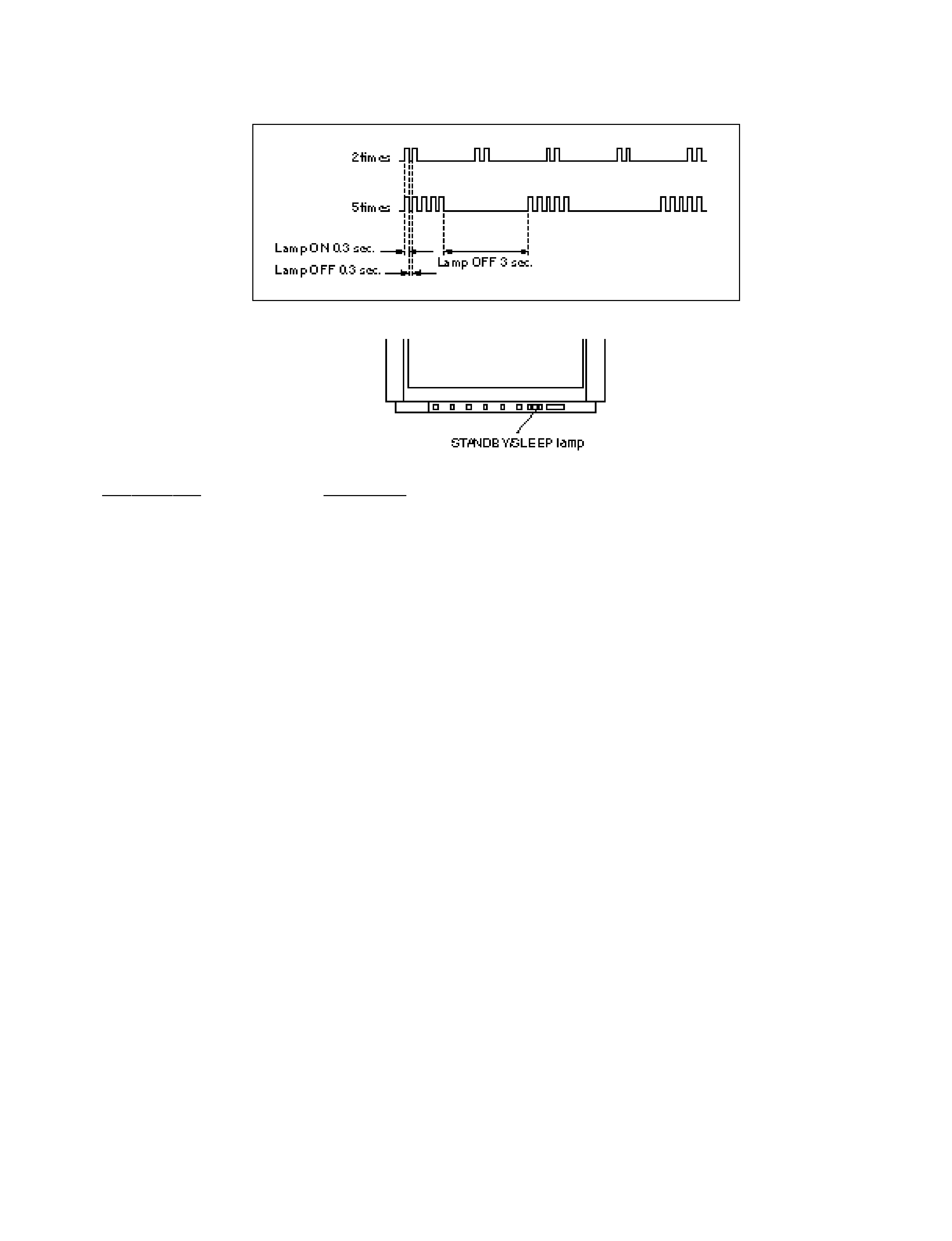
1.
DIAGNOSTIC TEST INDICATORS
When an errors occurs, the STANDBY/TIMER lamp will flash a set number of times to indicate the possible cause of the
problem. If there is more than one error, the lamp will identify the first of the problem areas.
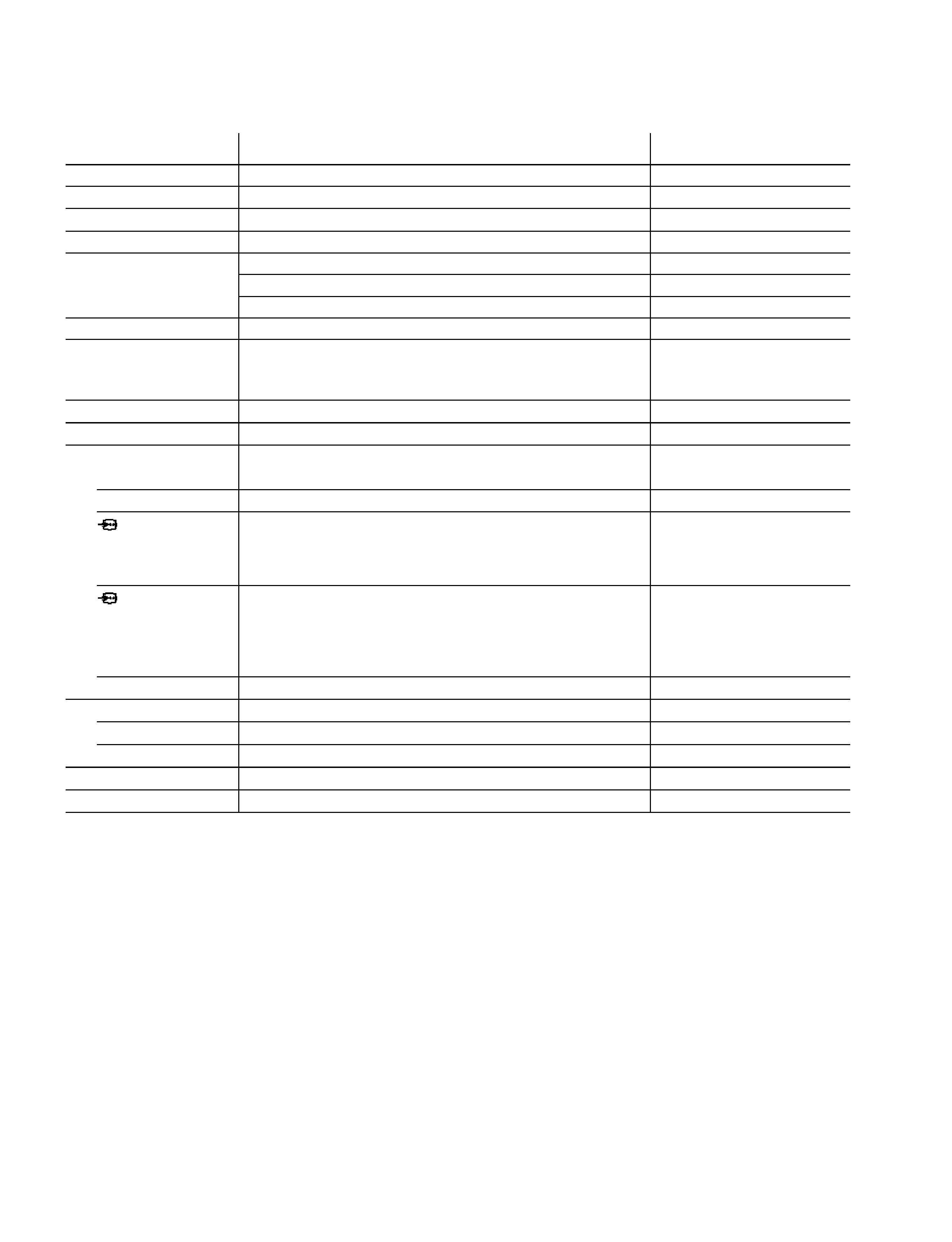
Result for all of the following diagnostic items are displayed on screen. No error has occured if the screen displays a "0".
Diagnostic
Item
Description
· Power does not
turn on
· +B overcurrent
(OCP) or
overvoltage
(OVP)
· Vertical deflection
stopped
· Horizontal
deflection
overdrive
· White balance
failure (no
PICTURE)
· Micro reset
No. of times
STANDBY/TIMER
lamp flashes
Does not light
2 times
5 times
--
Self-diagnostic
display/Diagnostic
result
--
002:000 or
002:001~255
003:001~255
004:001~255
at the same time
005:000 or
005:001~225
101:00 or
101:001~225
Probable
Cause
Location
· Power cord is not plugged
in.
· Fuse is burned out F4601
(F Board)
· H.OUT Q511 is shorted. (A
board)
· IC701 is shorted. (C board)
· -13V is not supplied. (A
board)
· IC 503 faulty (A board)
· G2 is improperly adjusted.
(Note 2)
· CRT problem.
· Video OUT IC701 is faulty.
(C board)
· IC301 is faulty. (A board)
· No connection A board to C
board.
· Discharge CRT (C Board)
· Static discharge
· External noise
Detected
Symptoms
· Power does not come on.
· No power is supplied to the
TV.
· AC power supply is faulty.
· Power does not come on.
· Load on power line is
shorted.
· Has entered standby state
after horizontal raster.
· Vertical deflection pulse is
stopped.
· Power line is shorted or
power supply is stopped.
· No raster is generated.
· CRT cathode current
detection reference pulse
output is small.
· Power is shut down shortly,
after this return back to
normal.
· Detect Micro latch up.
Note 1: If a + B overcurrent is detected, stoppage of the vertical deflection is detected simultaneously.
The symptom that is diagnosed first by the microcontroller is displayed on the screen.
Note 2: Refer to screen (G2) Adjustment in section 3-4 of this manual.
SELF DIAGNOSTIC FUNCTION
5
KV-EF34N90
RM-913
2.
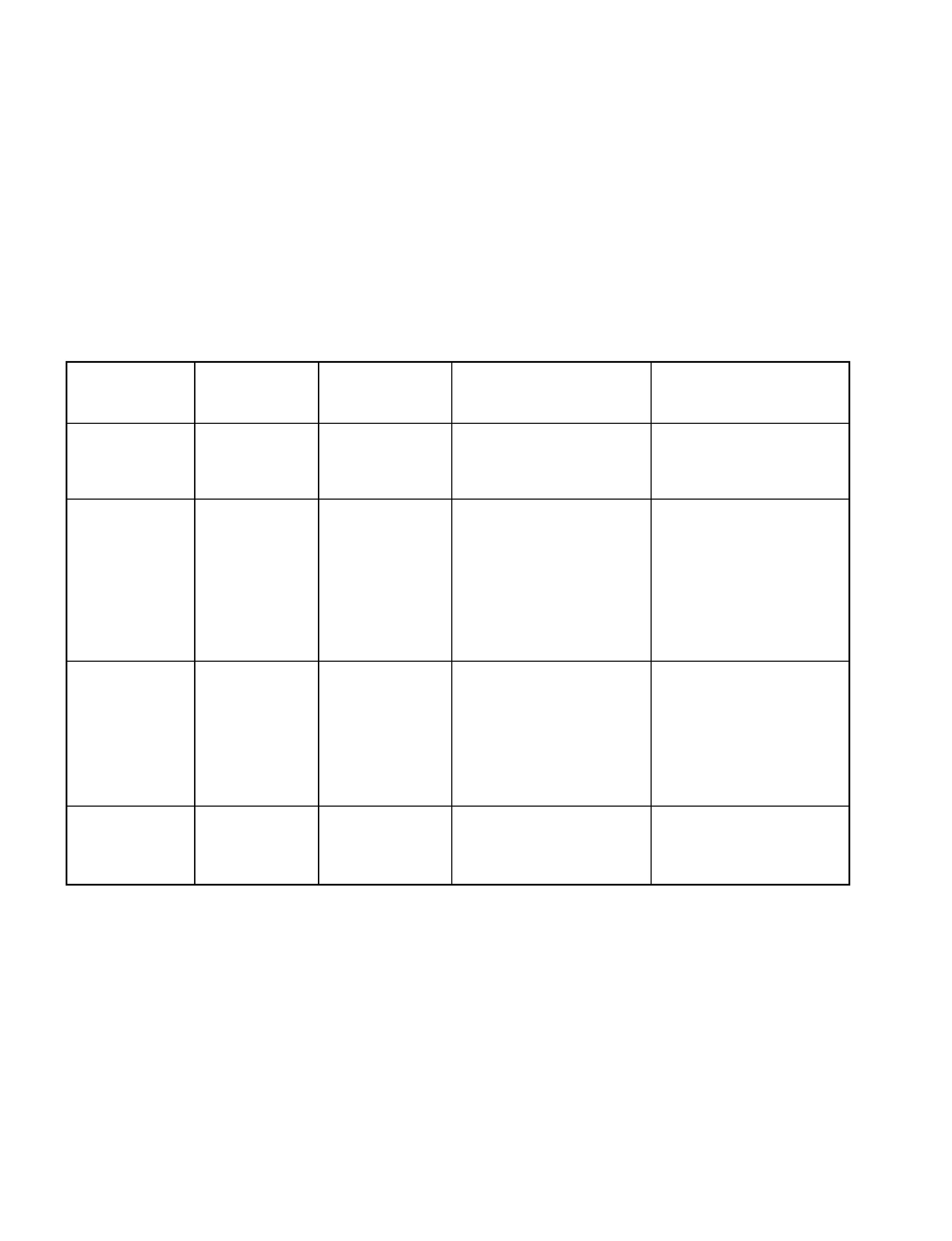
DISPLAY OF STANDBY/TIMER LIGHT FLASH COUNT
Diagnostic Item
Flash Count*
+B overcurrent/overvoltage
2 times
Vertical deflection stopped
White balance failure
5 times
* One flash count is not used for self-diagnostic.
3.
STOPPING THE STANDBY/TIMER FLASH
Turn off the power switch on the TV main unit or unplug the power cord from the outlet to stop the STANDBY/TIMER lamp
from flashing.