
LCD PROJECTION TELEVISION
SERVICE MANUAL
LA-3 CHASSIS
MODEL NAME
REMOTE COMMANDER
DESTINATION
9-965-974-05
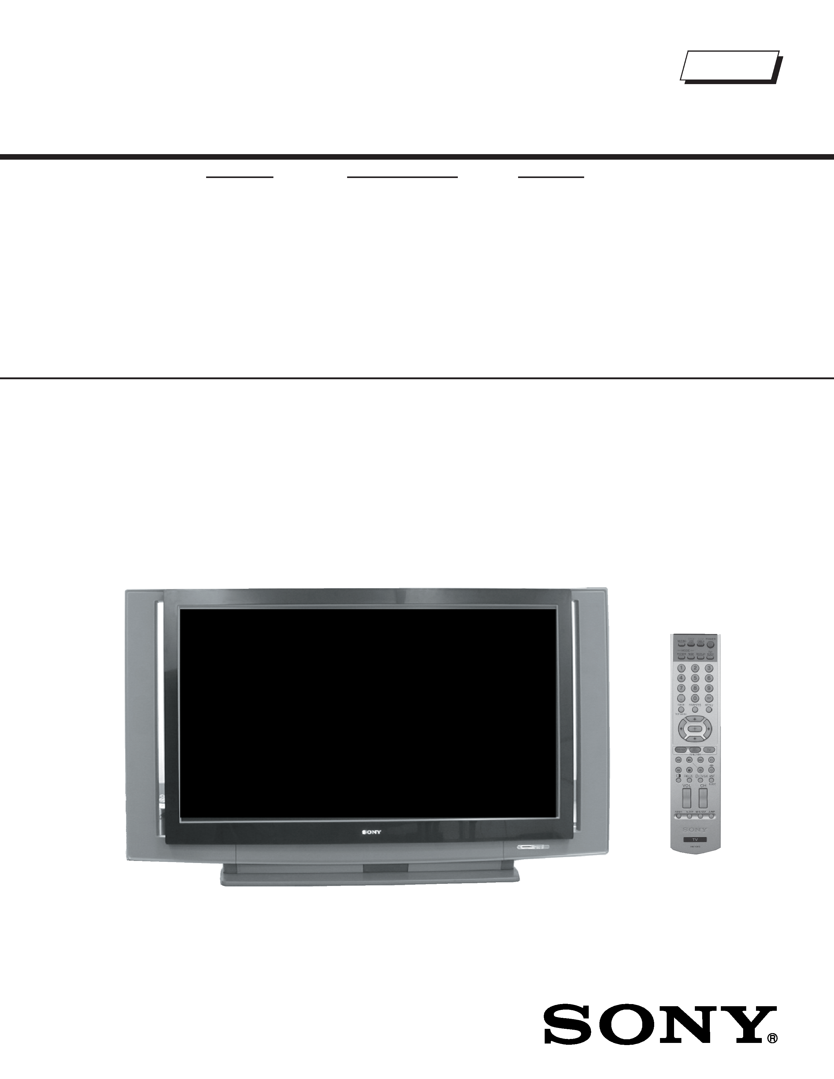
KDF-55XS955
RM-Y915
US/CND
KDF-60XS955
RM-Y915
US/CND
HISTORY INFORMATION FOR THE FOLLOWING MANUAL:
ORIGINAL MANUAL ISSUE DATE: 9/2004
:UPDATED ITEM
REVISION DATE
SUBJECT
9/2004
No revisions or updates are applicable at this time.
10/2004
Updated Block Diagram (Replaced Page 35 with Page 35)
1/2005
Corrected Section 2-1. Setting the Service Adjustment Mode and
2-2. Service Adjustment Mode Memory (Replaced Page 27 with Page 27)
Corrected Section 2-4. Remote Adjustment Buttons and Indicators (Replaced Page 28 with Page 28)
Updated contact information for Service Data requests (Replaced Page 30 with Page 30)
Updated contact information for Tiled Schematic requests (Replaced Last Page with Last Page)
1/2005
Added Caution statement (Replaced Page 6 with Page 6)
8/2005
Corrected location of LVDS Cables (Replaced Page 76 with Page 76)
LCD PROJECTION TELEVISION
SERVICE MANUAL
LA-3 CHASSIS
MODEL NAME
REMOTE COMMANDER
DESTINATION
9-965-974-05
KDF-55XS955
RM-Y915
US/CND
KDF-60XS955
RM-Y915
US/CND
Self Diagnosis
Supported model
KDF-55XS955
RM-Y915

3
KDF-55XS955/60XS955
KDF-55XS955/60XS955
TABLE OF CONTENTS
Specifications ................................................................................. 4
Warnings and Cautions .................................................................. 6
Safety Check-Out ........................................................................... 7
Self-Diagnostic Function................................................................. 8
SECTION 1: DISASSEMBLY............................................................... 13
1-1. Rear Cover Removal............................................................ 13
1-2. Center Pillar Removal .......................................................... 13
1-3. Chassis Assembly and Fan Removal .................................. 14
1-4. Service Position ................................................................... 14
1-5. Power Supply Block Removal (Lamp Drive Unit)................. 15
1-6. RF Antenna Switch and P Board Removal .......................... 15
1-7. U Board, H4 Board, and Fan Removal ................................ 16
1-8. F Board and G1 Board Board Removal ............................... 16
1-9. A Board and KD Board Removal.......................................... 17
1-10.Q Box Assembly and B Board Removal............................... 17
1-11. G2 Board Removal............................................................... 18
1-12.Woofer Removal .................................................................. 18
1-13.Optics Unit Block Assembly and D.C. Fan Removal............ 19
1-14.T Board Removal ................................................................. 19
1-15.Front Cover Assembly and H1 Board Removal ................... 20
1-15-1. Replacing the Lamp................................................. 20
1-16.HM Board and H2 Board Removal....................................... 20
1-17.H3 Board and Speaker Removal ......................................... 21
1-18.Screen Mirror Block Assembly Removal .............................. 21
1-19.Mirror Cover Assembly Removal.......................................... 22
1-19-1. Diffusion Plates (Screens) Tape Method ................. 22
Wire Dressing....................................................................... 23
SECTION 2: CIRCUIT ADJUSTMENTS.............................................. 27
2-1. Setting the Service Adjustment Mode .................................. 27
2-2. Service Adjustment Mode Memory ...................................... 27
2-3. Memory Write Confirmation Method .................................... 28
2-4. Remote Adjustment Buttons and Indicators ......................... 28
2-5. H/V Center Confirmation and Adjustments .......................... 29
2-6. Service Data......................................................................... 30
2-7. ID Map Table ........................................................................ 32
SECTION 3: DIAGRAMS..................................................................... 33
3-1. Circuit Boards Location ........................................................ 33
3-2. Printed Wiring Boards and
Schematic Diagrams Information ......................................... 33
3-3. Block Diagrams .................................................................... 35
3-4. Schematics and Supporting Information .............................. 36
A Board Schematic Diagram (1 of 3).................................... 36
A Board Schematic Diagram (2 of 3).................................... 37
A Board Schematic Diagram (3 of 3).................................... 38
B Board Schematic Diagram (1 of 6) ................................... 41
B Board Schematic Diagram (2 of 6) ................................... 42
B Board Schematic Diagram (3 of 6) ................................... 43
B Board Schematic Diagram (4 of 6) ................................... 44
B Board Schematic Diagram (5 of 6) ................................... 45
B Board Schematic Diagram (6 of 6) ................................... 46
G2 Board Schematic Diagram (1 of 2) ................................. 49
G2 Board Schematic Diagram (2 of 2) ................................. 50
P Board Schematic Diagram ............................................... 53
KD Board Schematic Diagram ............................................. 54
G1 Board Schematic Diagram (1 of 2) ................................. 56
G1 Board Schematic Diagram (2 of 2) ................................. 57
F Board Schematic Diagram ................................................ 60
HM Board Schematic Diagram............................................. 62
H1 Board Schematic Diagram.............................................. 64
H2 Board Schematic Diagram.............................................. 66
H3 Board Schematic Diagram.............................................. 68
H4 Board Schematic Diagram.............................................. 70
T Board Schematic Diagram ................................................ 70
U Board Schematic Diagram................................................ 71
3-5. Semiconductors ................................................................... 73
SECTION 4: EXPLODED VIEWS ........................................................ 74
4-1. Cover.................................................................................... 74
4-2. Bottom Cabinet .................................................................... 75
4-3. Chassis ................................................................................ 76
SECTION 5: ELECTRICAL PARTS LIST........................................... 77
SECTION TITLE
PAGE
SECTION TITLE
PAGE
4
KDF-55XS955/60XS955
KDF-55XS955/60XS955
SPECIFICATIONS
Design and specifications are subject to change without notice.
120V AC, 60Hz
265W
Under 20W
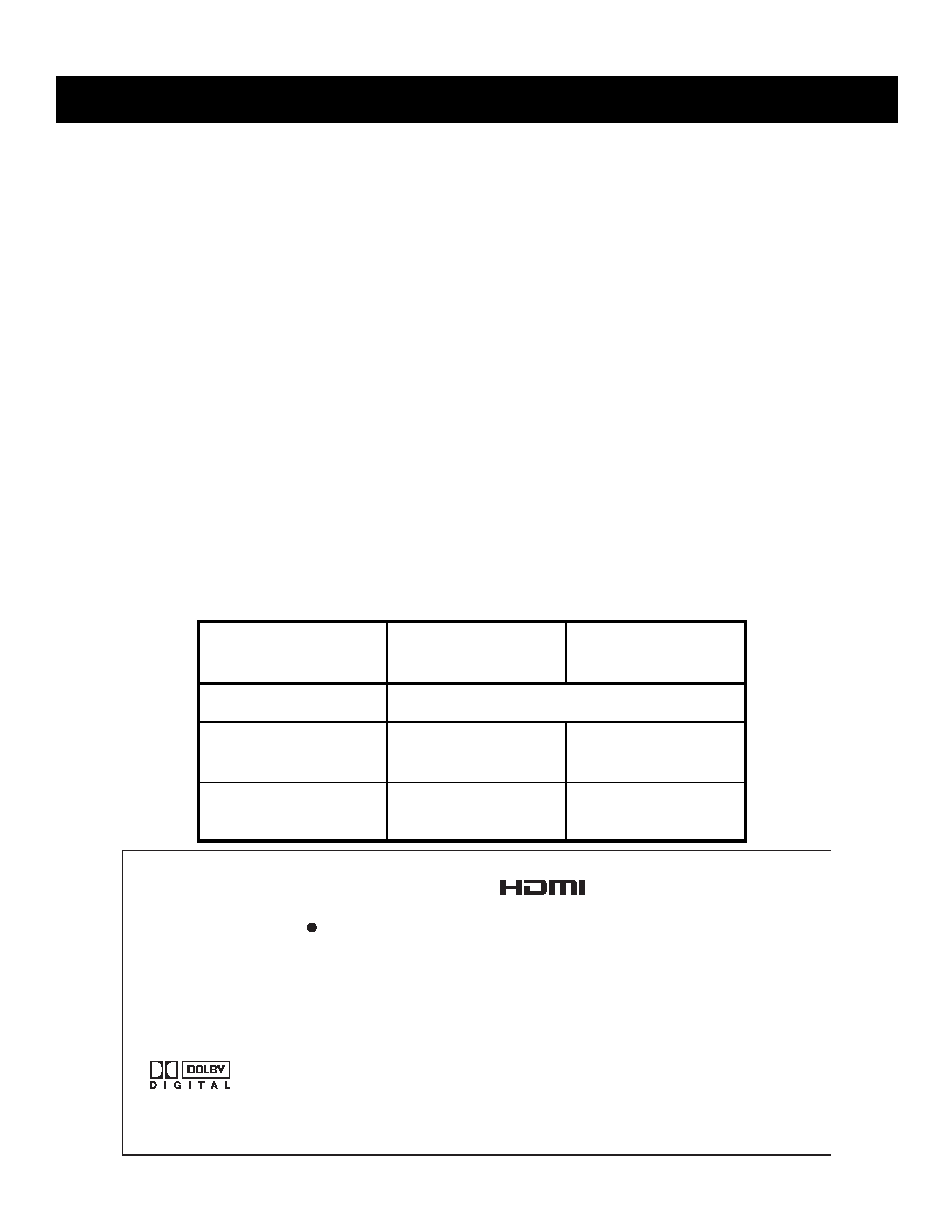
HDMI IN
2 total
Video - 1080i, 720p, 480p, 480i
Audio - Two channel linear PCM 32, 44.1 and 48 kHz,
16, 20, and 24 bit
Video (IN)
4 total (1 on front panel)
1Vp-p, 75ohms unbalanced, sync negative
S Video (IN)
4 total (1 on front panel)
Y: 1Vp-p, 75ohms unbalanced, sync negative
C: 0.286Vp-p (Burst signal), 75ohms
Audio (IN)
7 total (1 on front panel)
500 mVrms (100% modulation)
Impedance:47 kilo ohms
Audio (VAR/FIX) Out
1 total
500 mVrms at the maximum volume setting (Variable)
500 mVrms (Fixed)
Impedance (Output):2 kilo ohm
Note: Audio Out jacks are operable only when
the TV's speaker is set to Off.
Power Requirements
Power Consumption (W)
In Use (Max)
In Standby
Inputs/Outputs
Control S (IN)
1 total
Minijack
Control S (OUT)
1 total
Minijack
Component Video Input
2 (Y, P
B, PR)
Y: 1.0 Vp-p, 75 ohms unbalanced, sync negative
P
B
: 0.7 Vp-p, 75 ohms;
P
R: 0.7 Vp-p, 75 ohms
RF Inputs
2 total
Digital Audio Optical Output (PCM/Dolby Digital)
1 total
Optical Rectangular (1)
CableCARD Slot
1 total
PCMCIA Type I/II
CableCARD
TM is a trademark of Cable Television
Laboratories, Inc.
TruSurround, SRS and the ( )® symbol are trademarks
of SRS Labs, Inc.
TruSurround technology is incorporated under license
from SRS Labs, Inc.
BBE and BBE Symbol are trademarks of BBE Sound,
Inc. and are licensed by BBE Sound, Inc. under U.S.
Patent No. 4,638,258 and 4,482,866.
Manufactured under license from
Dolby Laboratories Licensing
Corporation. Dolby and the double-D
symbol are trademarks of Dolby
Laboratories Licensing Corporation.
This TV incorporates High-Definition
Multimedia Interface (HDMI
TM)
technology. HDMI, the HDMI logo
and High-Definition Multimedia
Interface are trademarks or registered
trademarks of HDMI Licensing LLC.
WEGA, Steady Sound, Digital Reality Creation,
CineMotion, Memory Stick, Memory Stick Duo,
Memory Stick PRO, Memory Stick PRO Duo,
MagicGate, MID and Twin View are trademarks of Sony
Corporation.
KDF-55XS955
KDF-60XS955
Speaker Output (W)
Woofer
Dimensions (W x H x D)
mm
1,574 x 952 x 484 mm
1,685 x 1,007 x 514 mm
in
62 x 37
1/2 x 19 in
66
3/8 x 39 5/8 x 20 1/4 in
Mass
kg
48 kg
51.5 kg
lbs
105 lbs 29 oz
113 lbs 19 oz
5W x 2
20W

5
KDF-55XS955/60XS955
KDF-55XS955/60XS955
Television system
American TV standard, NTSC
ATSC compliant 8VSB, ATSC (8VSB terrestrial)
ANSI/SCTE 07 2000 QAM on cable
Channel coverage
Terrestrial 2-69/ Cable TV: 1-125 (analog)
Terrestrial: 2-69/ Cable TV: 1-135 (digital)
Screen Size (measured diagonally)
55 inches (KDF-55XS955 Only)
60 inches (KDF-60XS955 Only)
Antenna
75-ohm external antenna terminal for VHF/UHF
Projection System
3 LCD Panels, 1 lens projection system
LCD Panel
0.87 inch TFT LCD panel Approx. 3.28 million dots
(1,042,168 pixels)
Projection Lens
High Performance, large diameter hybrid lens F2.4
Lamp
UHP lamp, 132W XL-2100
Supplied Accessories
Remote Commander RM-Y915
Two Size AA (R6) Batteries