1
SERVICE MANUAL
ICF-CD831/CD831L
CD player section
System:
Compact disc digital audio system
Laser diode properties:
Material: GaAlAs
Wavelength: 780 nm
Emission duration: Continuous
Laser output: Less than 44.6 µW
(This output is the value measured at a distance of
about 200 mm from the objective lens surface on
the optical pick-up block with 7 mm aperture.)
Frequency response:
20 - 20,000 Hz
dB
Wow and flutter:
Below measurable limit
SPECIFICATIONS
Radio section
Frequency range:
ICF-CD831
ICF-CD831L
CND, AUS, MX model
FM
87.5 - 108 MHz
--
AM
530 - 1,710 kHz
--
IT model
FM
87.5 - 108.0 MHz
--
AM
526.5 - 1,606.5 kHz
--
AEP, UK model
FM
87.5 - 108 MHz
87.5 - 108 MHz
AM (MW)
530 - 1,710 kHz
530 - 1,605 kHz
LW
--
153 - 255 kHz
Ver 1.1 2003. 04
9-877-189-02
2003D0400-1
© 2003. 04
Canadian Model
Australian Model
Italian Model
Mexican Model
ICF-CD831
AEP Model
UK Model
ICF-CD831L
CD
Model Name Using Similar Mechanism CFD-S200/S200L
Section
CD Mechanism Type
KSM-213RDP
Optical Pick-up Name
KSS-213R
Sony Corporation
Personal Audio Company
Published by Sony Engineering Corporation
FM/AM CD CLOCK RADIO
ICF-CD831
FM/MW/LW CD CLOCK RADIO
ICF-CD831L
Photo: ICF-CD831
Continued on next page
+1
1.5

2
ICF-CD831/CD831L
SAFETY-RELATED COMPONENT WARNING!!
COMPONENTS IDENTIFIED BY MARK 0 OR DOTTED LINE
WITH MARK 0 ON THE SCHEMATIC DIAGRAMS AND IN
THE PARTS LIST ARE CRITICAL TO SAFE OPERATION.
REPLACE THESE COMPONENTS WITH SONY PARTS WHOSE
PART NUMBERS APPEAR AS SHOWN IN THIS MANUAL OR
IN SUPPLEMENTS PUBLISHED BY SONY.
Flexible Circuit Board Repairing
· Keep the temperature of the soldering iron around 270°C during
repairing.
· Do not touch the soldering iron on the same conductor of the
circuit board (within 3 times).
· Be careful not to apply force on the conductor when soldering
or unsoldering.
Notes on Chip Component Replacement
· Never reuse a disconnected chip component.
· Notice that the minus side of a tantalum capacitor may be dam-
aged by heat.
NOTES ON HANDLING THE OPTICAL PICK-UP BLOCK
OR BASE UNIT
The laser diode in the optical pick-up block may suffer electrostatic
breakdown because of the potential difference generated by the
charged electrostatic load, etc. on clothing and the human body.
During repair, pay attention to electrostatic breakdown and also use
the procedure in the printed matter which is included in the repair
parts.
The flexible board is easily damaged and should be handled with
care.
NOTES ON LASER DIODE EMISSION CHECK
The laser beam on this model is concentrated so as to be focused on
the disc reflective surface by the objective lens in the optical pick-
up block. Therefore, when checking the laser diode emission,
observe from more than 30 cm away from the objective lens.
ATTENTION AU COMPOSANT AYANT RAPPORT
À LA SÉCURITÉ!!
LES COMPOSANTS IDENTIFIÉS PAR UNE MARQUE 0 SUR LES
DIAGRAMMES SCHÉMATIQUES ET LA LISTE DES PIÈCES SONT
CRITIQUES POUR LA SÉCURITÉ DE FONCTIONNEMENT. NE
REMPLACER CES COMPOSANTS QUE PAR DES PIÈCES SONY
DONT LES NUMÉROS SONT DONNÉS DANS CE MANUEL OU
DANS LES SUPPLÉMENTS PUBLIÉS PAR SONY.
General
Time display:
CND, UK, AUS, MX model:
12-hour system
AEP, IT model: 24-hour system
Speaker:
66 mm (2 5 /8 inches) dia., 8
Power outputs:
1 W + 1 W (at 10% harmonic distortion)
Power requirements:
CND, MX model:
120 V AC, 60 Hz
AEP, UK, AUS model: 230 V AC, 50 Hz
Dimensions:
Approx. 229
× 104 × 218 mm (w/h/d)
(Approx. 9 1 /8
× 4 1 /8 × 8 5 /8 inches)incl.
projecting parts and controls
Mass:
Approx. 1,650 g (3 lb. 10 oz.)
UK model: Approx. 1,700 g (3 lb. 12 oz.)
Design and specifications are subject to change without
notice.
·Abbreviation
CND
: Canadian model
AUS: Australian model
IT
: Italian model
MX
: Mexican model
This Compact Disc player is classified as a CLASS 1
LASER product.
The CLASS 1 LASER PRODUCT label is located on
the bottom exterior.
CAUTION
Use of controls or adjustments or performance of proce-
dures other than those specified herein may result in haz-
ardous radiation exposure.
Ver 1.1

3
TABLE OF CONTENTS
1. SERVICING NOTES
1-1. Cord Dressing (Power Cord) ............................................... 5
1-2. Pointer Alignment ............................................................... 5
2. GENERAL ............................................................................ 6
3. DISASSEMBLY
3-1. Cabinet (Upper) Assy .......................................................... 7
3-2. Lid (CD) .............................................................................. 8
3-3. Chassis Assy ........................................................................ 8
3-4. Main Board, Drive Board .................................................... 9
3-5. Key (A) Board, Key (B) Board ........................................... 9
3-6. CD Mechanism Deck ........................................................ 10
3-7. Optical Pick-up ................................................................. 10
4. ELECTRICAL ADJUSTMENTS
Tuner Section ......................................................................... 11
CD Section ............................................................................ 13
5. DIAGRAMS
5-1. IC Pin Description ............................................................. 15
5-2. Circuit Boards Location .................................................... 15
5-3. Block Diagram CD Section ......................................... 16
5-4. Block Diagram Tuner Section ..................................... 17
5-5. Block Diagram Main Section ...................................... 18
5-6. Printed Wiring Board CD Section ............................... 19
5-7. Schematic Diagram CD Section .................................. 20
5-8. Schematic Diagram Main Section ............................... 21
5-9. Printed Wiring Board Main Section (ICF-CD831) ..... 22
5-10. Printed Wiring Board Main Section (ICF-CD831L) ... 23
5-11. Schematic Diagram Control, Display Section ............ 24
5-12. Printed Wiring Boards Key Section ............................ 25
5-13. Printed Wiring Board Drive Section ........................... 26
5-14. Printed Wiring Board Transformer Section ................. 27
5-15. IC Block Diagrams ............................................................ 28
6. EXPLODED VIEWS
6-1. Cabinet (Upper) Section .................................................... 29
6-2. Cabinet (Lower) Section ................................................... 30
6-3. Chassis Section ................................................................. 31
6-4. CD Mechanism Section .................................................... 32
7. ELECTRICAL PARTS LIST ......................................... 33
ICF-CD831/CD831L
4
ICF-CD831/CD831L
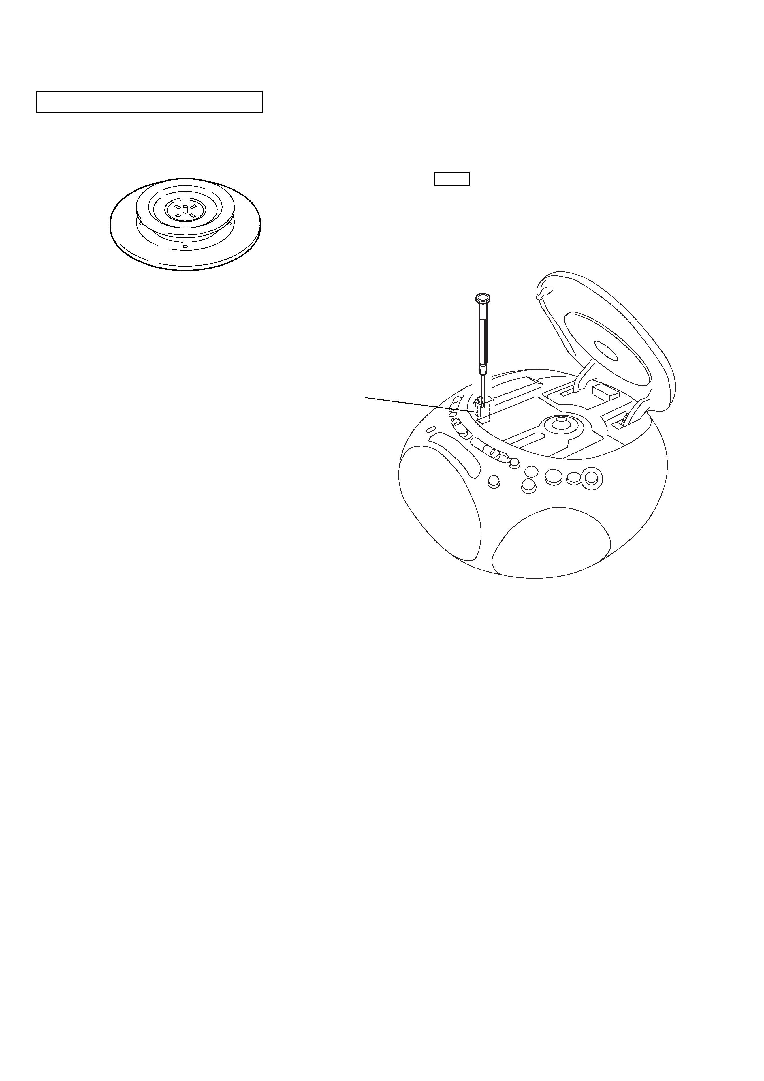
CHUCK PLATE JIG ON REPAIRING
On repairing CD section, playing a disc without the lid (CD), use
Chuck Plate Jig.
· Code number of Chuck Plate Jig: X-4918-255-1
SECTION 1
SERVICING NOTES
LASER DIODE AND FOCUS SEARCH OPERATION
CHECK
1. Turn ON the [POWER] button and press [CD] button to CD
position.
2. Open the CD lid.
3. Turn on S401 with screwdriver, etc. as following figure.
4. Press the N X (CD) button.
5. Confirm the laser diode emission while observing the objecting
lens. When there is no emission, Auto Power Control circuit or
Optical Pick-up is broken.
Objective lens moves up and down three times for focus search.
S401
5
ICF-CD831/CD831L
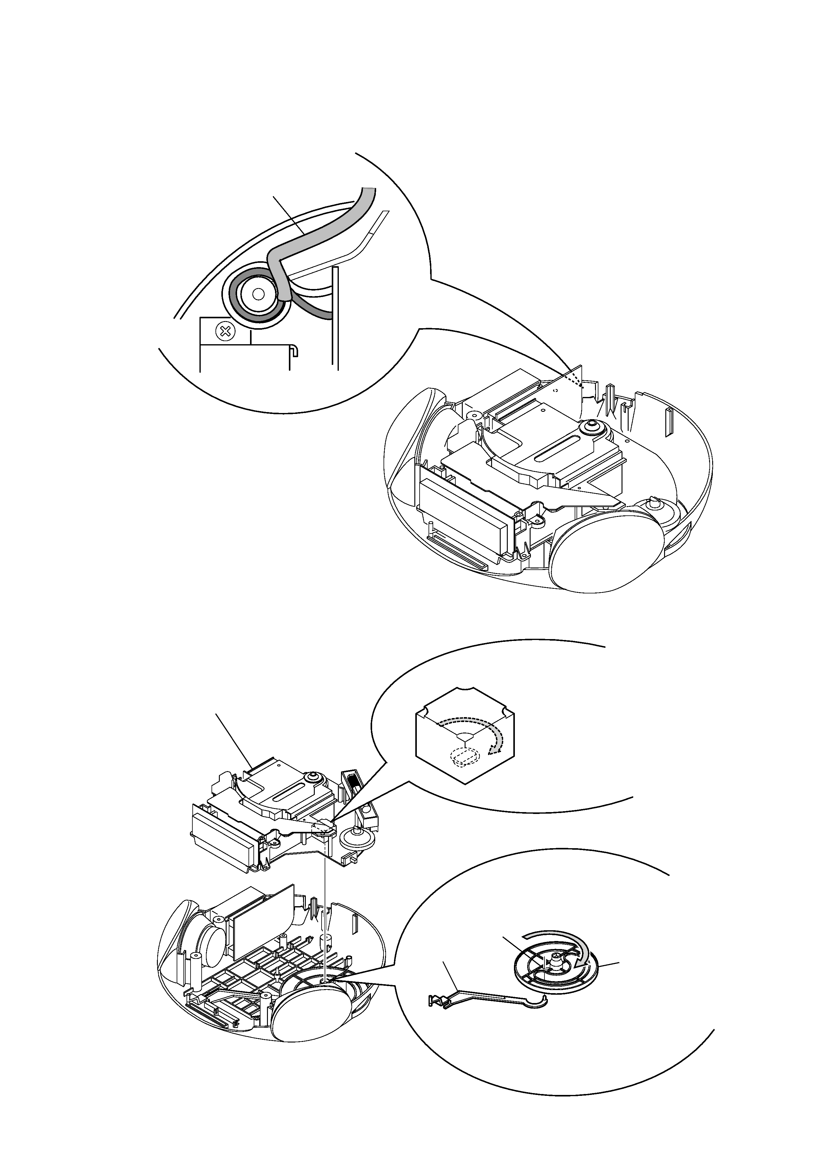
1-1. CORD DRESSING
(POWER CORD)
1) Set the power cord as shown in the figure.
pointer
2
Fit the protrusion on the
pointer in the hole A.
3
Align the notch on the
boss of the knob (tune)
with the direction of CV1.
knob (tune)
chassis assy
1
Turn this in the arrow direction
until stopped.
A
power cord
1-2. POINTER ALIGNMENT