MICROFILM
SERVICE MANUAL
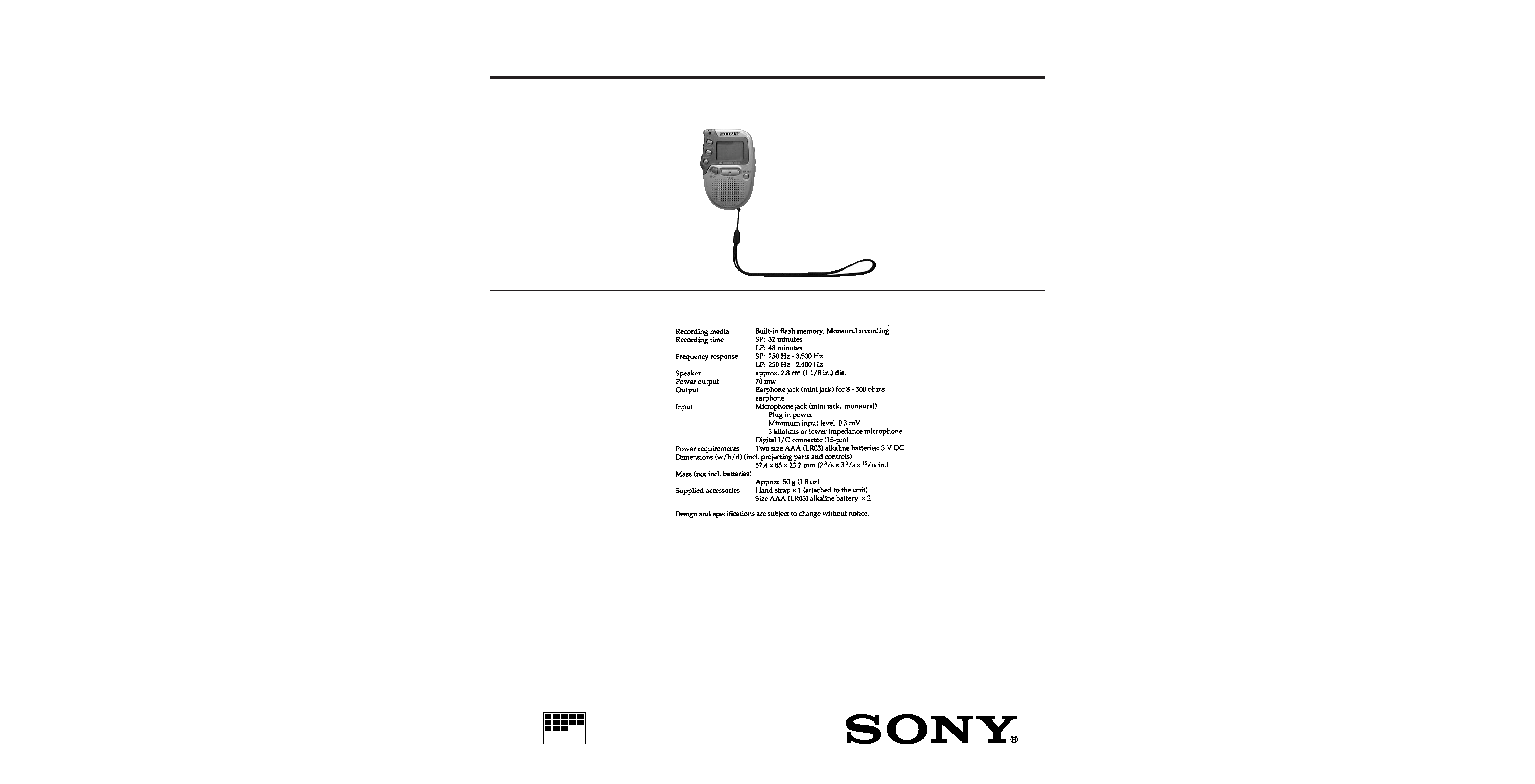
IC RECORDER
US Model
SPECIFICATIONS
ICD-80
Ver 1.0 1998. 07

2
TABLE OF CONTENTS
1.
SERVICING NOTES ............................................... 2
2.
GENERAL ................................................................... 3
3.
DISASSEMBLY ......................................................... 4
4.
DIAGRAMS
4-1. Block Diagram ................................................................
5
4-2. Schematic Diagram .........................................................
8
4-3. Printed Wiring Board ...................................................... 11
4-4. IC Pin Function Description ........................................... 16
5.
EXPLODED VIEW ................................................... 19
6.
ELECTRICAL PARTS LIST ............................... 20
SECTION 1
SERVICING NOTES
CAUTION ON REPLACING FLASH MEMORY
The BAD-BLOCK check* must be executed, when the flash
memory in this set was replaced.
The set will not operate normally, unless this check is finished.
* The BAD-BLOCK check detects an area (bad-block) in the flash
memory where data validity cannot be guaranteed, and saves
this information in the TOC-AREA so that a bad-block is not
used.
BAD-BLOCK Check Procedure:
1. Apply 3.0 V from regulated power supply to the battery termi-
nals.
(The battery lid open/close detection switch S701 may be kept
off)
2. Red LED and green LED light up.
3. As "Push St & Er" is displayed on the LCD, press the STOP
(S703) button and the ERASE (S702) button simultaneously.
(BAD-BLOCK check will start)
4. "Bad Check" is displayed on the LCD. (Check will last for
about 90 sec, and keep applying regulated power supply dur-
ing checking)
5. Backlight turns on (BAD-BLOCK check finished successfully)
(*)
Red and green LEDs turn off. "Good OK!" is displayed on
the LCD.
(*): In case of NG, "Bad Memory" is displayed on the LCD.
6. Press the RESET (S501) button.
Note:
· In case of NG, check the System Control IC, Memory IC, and
their peripheral circuits. (Particularly, check carefully the sol-
dering of the flash memory)
· After finishing the BAD-BLOCK check, assemble the set, load
the battery, and confirm if the set operates normally.
Flexible Circuit Board Repairing
· Keep the temperature of the soldering iron around 270 °C dur-
ing repairing.
· Do not touch the soldering iron on the same conductor of the
circuit board (within 3 times).
· Be careful not to apply force on the conductor when soldering
or unsoldering.
Notes on chip component replacement
· Never reuse a disconnected chip component.
· Notice that the minus side of a tantalum capacitor may be dam-
aged by heat.
3
SECTION 2
GENERAL
This section is extracted from
instruction manual.
4
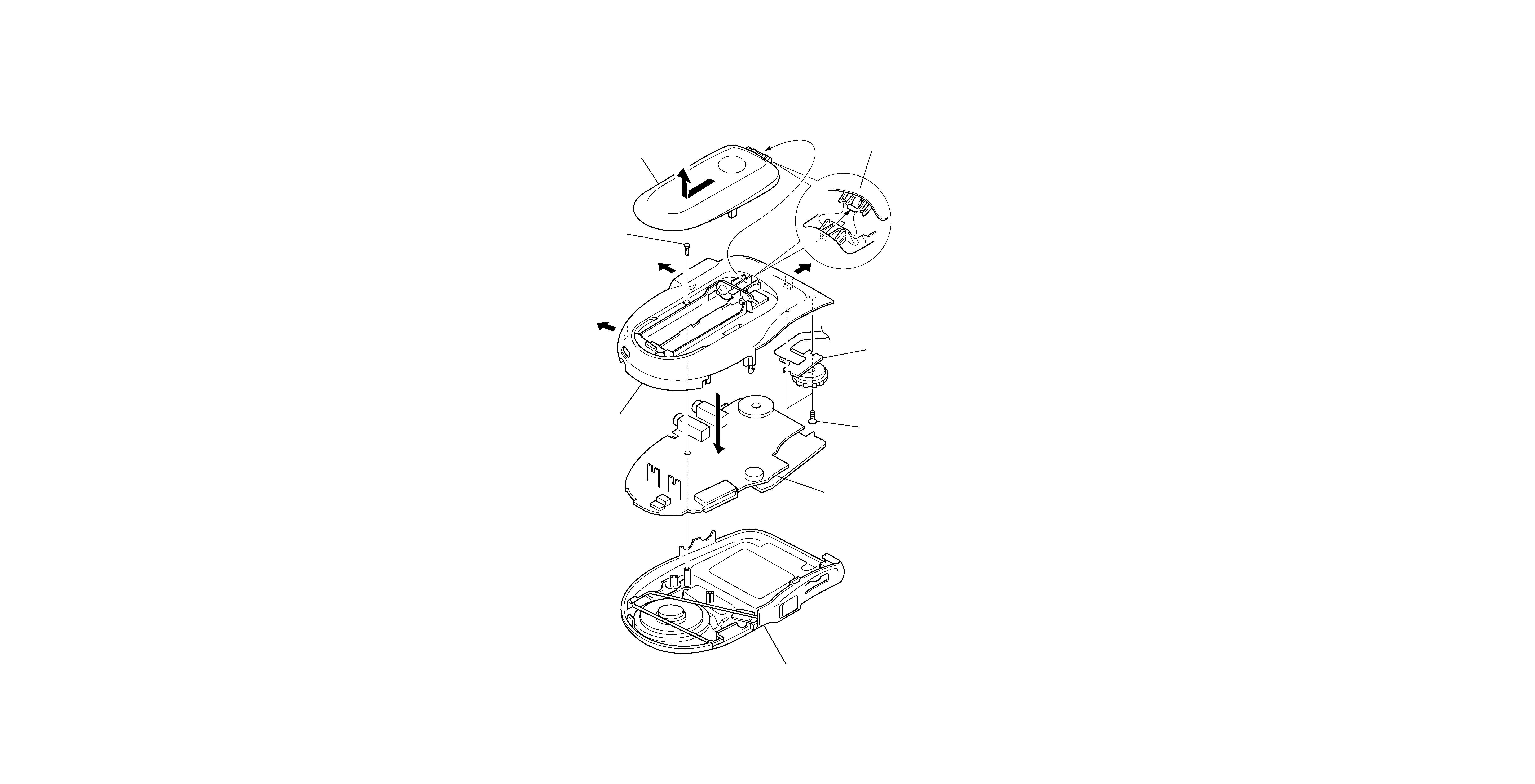
BATTERY CASE LID, MAIN BOARD
Note: Follow the disassembly procedure in the numerical order given.
SECTION 3
DISASSEMBLY
1 battery case lid
A
2 tapping screw
(B1.7)
7 case block assy
3 upper lid block assy
4 MAIN board
5 two screws
(M1.7
× 2.5)
6 switch unit
Pull the battery case lid toward
direction
A, remove it.
ICD-80
5
6
7
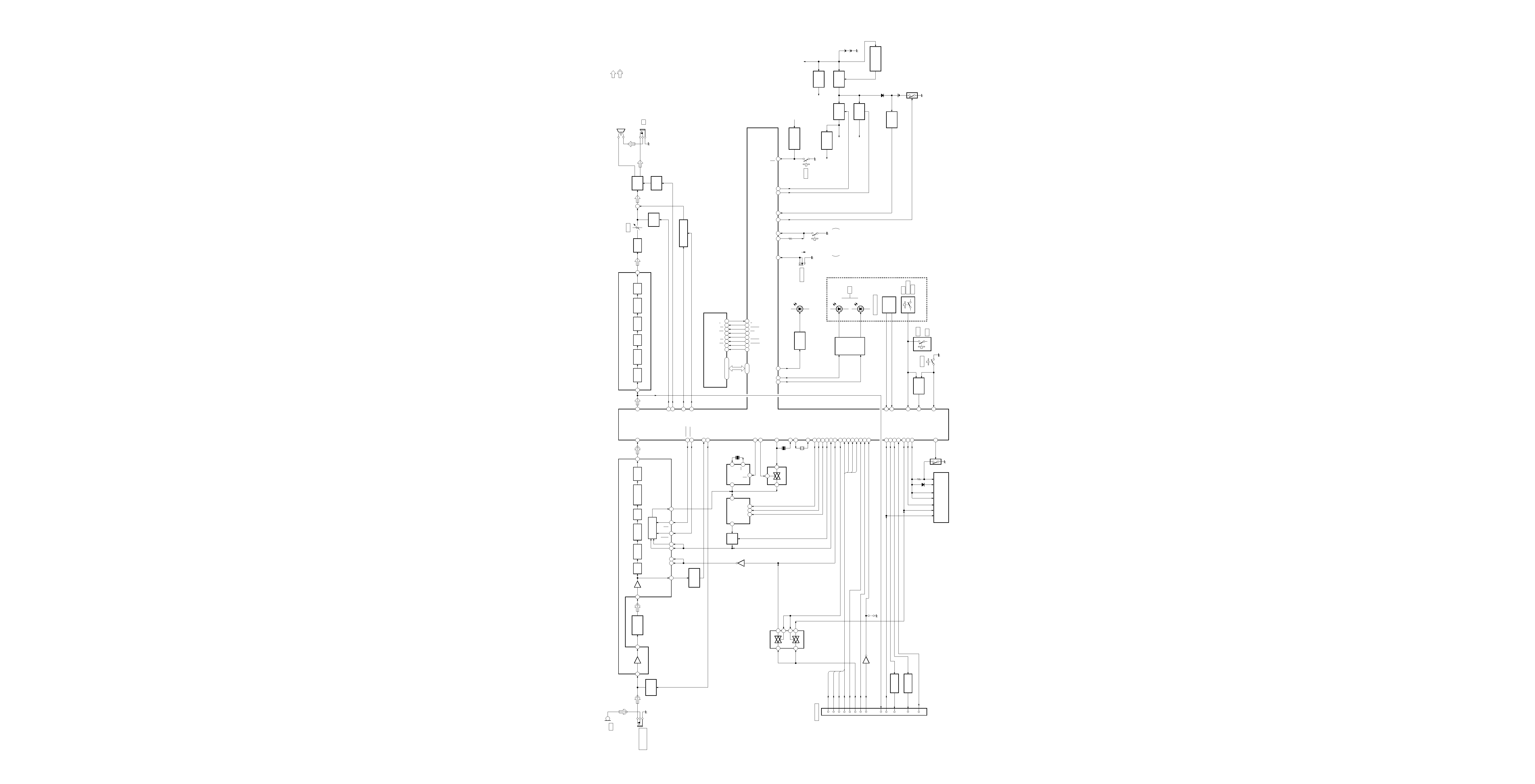
4-1.
BLOCK DIAGRAM
SECTION 4
DIAGRAMS
12
13
J101
MIC
PLUG IN POWER
MIC101
MIC
SP101
(SPEAKER)
J102
(EARPHONE)
@
MIC SENSE
SWITCH
Q103
AGC CIRCUIT
D101, D102,
IC103, Q104
VOR
DETECTOR
IC104
LEVEL SHIFT
Q704 (1/2)
DATA
LATCH
IC107
DECIMETER
TIMING
GENERATOR
L.P.F.
B.P.F.
COMPRESSOR
ADPCM
DECODER
A/D
CONVETER
INTER-
POLATOR
L.P.F.
D/A
CONVETER
L.P.F.
TONE
CONTROL
LINE
MUTING
Q105
VOLTAGE
DETECTOR
IC503
DC/DC
CONVERTER
IC504
DC/DC CONVERTER
CONTROL
IC505, Q502
+3.3V
REGULATOR
IC501
+2.1V
REGULATOR
IC551
REGULATOR
Q101, 102
RESET SIGNAL
GENERATOR
IC502
B+
SWITCH
Q501
GAIN DOWN MUTING
Q107
BACK LIGHT
LED DRIVE
Q503
D503
(BACK LIGHT)
SWITCH UNIT
(PLAY: GREEN)
(REC: RED)
(PUSH: PLAY/STOP)
POWER
AMP
IC105
STANDBY
SWITCH
Q106
EXPANDER
ADPCM
DECODER
LEVEL SHIFT
Q704 (2/2)
AIN1
GSX1
14
15
AIN2
GSX2
27
BCLKA
28
BCLKB
26
XSYNC
25
RSYNC
1
13
RESET
21
PDN
1
INH
24
MCK
9
CLK
10
DATA
11
CE
5
IS
16
VFRO
OUT
4
2
1
4
24
23
OUT
2
XT
6
XT
1296 DIVIDER
IC106
ADPCM
IC101 (1/2)
ADPCM
IC101 (2/2)
FLASH MEMORY
IC702
SYSTEM CONTROLLER
IC701
IC102
X702
6.912MHz
X703
10.368MHz
X701
32.768kHz
CLOCK SWITCH
IC703
OSCO
46 POS LE
44 POS DAT
45 POS CLK
65 PO XSDW
76 XSYNC
67 POA CLK
33 PO WLOK
39 PI COM0
70 POD SCK
71 POD STB
60
63
PO LCDV
KEY A/D
52 PO LCDR
57 PO SPC
58 PO LPC
PO0 PO7
I/O0 I/O7
3 POA PDN
4 POA RES
10 PI VOR
68 PIA IS
69
POA IR
12
PO MUTE
51
PO PAMP
53
PO BEEP
1
PO PMUT
93
POR
CLE
2
CLE
94
POR
ALE
3
ALE
95
4
96
42
98
SE
30
PO
LIGH
9
PI
HOLD
40
SE
99
5
LED DRIVE
Q551
ROTARY
ENCODER
KEY
WAKE-UP
Q701 703
27
POL
PLY
26
POL
REC
6
43
WE
RE
WP
CE
7
41
R/B
4
IR
5
PO MIC
OSCI
40 PI COM1
41 PI COM2
42 PI COM3
77 PI REQ
50 PI C/D
48 PI TEST
32 PO OPT
38 PI WLNK
21
20
XO
XI
CLOCK GENERATOR
IC704
1
IN
6
5
3
CLOCK SWITCH
IC705
Q705
1
2
7
78
PI WAKE
8
PI ERS
81
PI POTB
80
PI POTA
72 POD DAT
31 PO ACK
D701
SCK
STB
VDD
VDD2
VLCD
VREF
DATA
REFERENCE
VOLTAGE
SWITCH
Q706
LCD MODULE
BP701
8
9
10
11
12
13
7
1
2
3
4
5
6
DATA0 (COM0)
DATA1 (COM1)
DATA2 (COM2)
DATA3 (COM3)
DATA4 (REQUEST)
DATA5 (SCLK)
DATA6 (C/D)
DATA7 (TEST)
DATA0
DATA1
DATA2
DATA3
DATA0
DATA1
DATA2
DATA3
STATUS4 (SDATAO)
STATUS5 (SDATAI)
STATUS6 (OPT)
STATUS7 (ACK)
GND (WAV LINK)
CN703
DIGITAL I/O
+
RV101
VOL
POR
CE
WP
POR
RE
POR
WE
84 91
18 21, 24 27
S702
ERASE
S703
STOP
FILE
OPR
= + +
PRIORITY
MENU
S705
REC
56
PO
BOP
79
PI
OPEN
14
PO
BACK
13
PO
BOT
15
PO
REGU
11
PI
DET3
82
RST
OFF
ON
9 HOLD
S704
DRY BATTERY
SIZE "AAA"
(IEC DESIGNATION R03)
2PCS. 3V
POWER AMP
(IC105) B+
+2.1V
LED B+
MIC CIRCUIT B+
+3.3V
BACK UP B+
BACK UP B+
D501
BT501
BACK UP
CONTROL
SWITCH
Q552
S501
RESET
· SIGNAL PATH
: PLAY
: REC
S701
BATTERY LID
OPEN/CLOSE DETECT
PIR
R/B