ICD-70
US Model
Canadian Model
AEP Model
E Model
Tourist Model
SERVICE MANUAL
IC RECORDER
MICROFILM
SPECIFICATIONS
Recording media
Built-in flash memory, Monaural recording
Recording time
SP : 16 minutes
LP : 24 minutes
Frequency response
SP : 250 Hz - 3,500 Hz
LP : 250 Hz - 2,400 Hz
Speaker
approx. 2.8 cm (1
1/8 in.) dia.
Power output
70 mw
Output
Earphone jack (mini jack) for 8 - 300 ohms
earphone
Input
Microphone jack (mini jack, monaural)
Plug in power
Minimum input level 0.3 mV
3 kilohms or lower impedance microphone
Digital I/O connector (15-pin)
Power requirements
Two size AAA (LR03) alkaline batteries : 3V DC
Dimensions (w/h/d) (incl. projecting parts and controls)
57.4
× 85 × 23.2 mm (23/8 × 33/8 × 15/16 in.)
Weight (not incl. batteries)
Approx. 50g (1.8 oz)
Supplied accessories
Hand strap
× 1 (attached to the unit)
Size AAA (LR03) alkarine battery
× 2
Optional accessories
Active speakers SRS-T1
Connecting cable RK-G64HG
WAV LINK software (available in spring '98)
· For IBM PC/AT* or compatible PC
· For Windows® 95/Windows® 3.1**(English
version)
· To play back messages on the computer, a
sound board must be installed in the
computer.
Design and specifications are subject to change without notice.
* IBM PC/AT is a registered trademark of International Business
Machines Corporation of the U.S.A.
** Windows® 95 and Windows® 3.1 are registered trademarks licensed
to Microsoft Corporation, registered in the U.S.A. and other
countries.

-- 2 --
TABLE OF CONTENTS
SERVICE NOTE
Notes on chip component replacement
· Never reuse a disconnected chip component.
· Notice that the minus side of a tantalum capacitor may be damaged
by heat.
Flexible Circuit Board Repairing
· Keep the temperature of soldering iron around 270 °C during
repairing.
· Do not touch the soldering iron on the same conductor of the
circuit board (within 3 times).
· Be careful not to apply force on the conductor when soldering or
unsoldering.
SERVICING NOTE ······················································ 2
1.
GENERAL ······································································ 3
2.
DISASSEMBLY
2-1.
BATTERY CASE LID, MAIN board ································· 5
3.
DIAGRAMS
3-1.
IC Pin Functions ································································· 6
3-2.
Printed Wiring Board -- MAIN Section -- ······················· 8
3-3.
Schematic Diagram -- MAIN Section -- ························ 11
3-4.
IC Block Diagrams ··························································· 15
4.
EXPLODED VIEWS
4-1.
Main Section ····································································· 18
5.
ELECTRICAL PARTS LIST ··································· 19
-- 3 --
SECTION 1
GENERAL
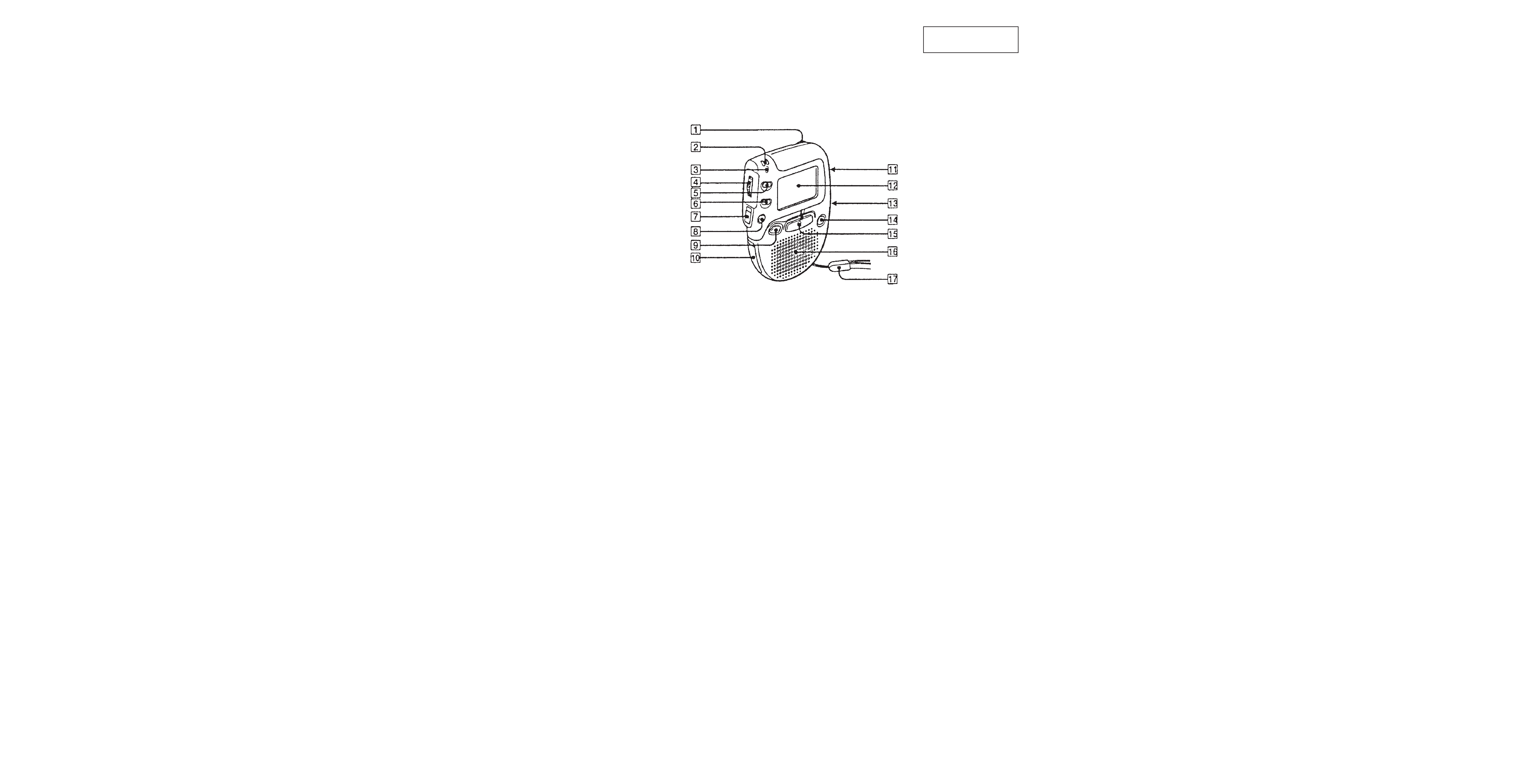
1 VOL knob
2 MIC
3 OPR indicator light
4 JOG DIAL switch (PLAY/STOP) (=/+ FF/REW)
(
/
select on MENU mode)
5 FILE button
6 PRIORITY button
7 C HOLD switch
8 MENU button
9 STOP button
!º DIGITAL I/O connector (for personal computer)
!¡ @ (EARPHONE) jack
!TM LIQUID CRYSTAL DISPLAY PANEL
!£ MIC (PLUG IN POWER) jack
!¢ ERASE button
! REC button
!§ SPEAKER
!¶ HAND STRAP
This section is extracted
from instruction manual.
C
c
IC RECORDER
-- 4 --
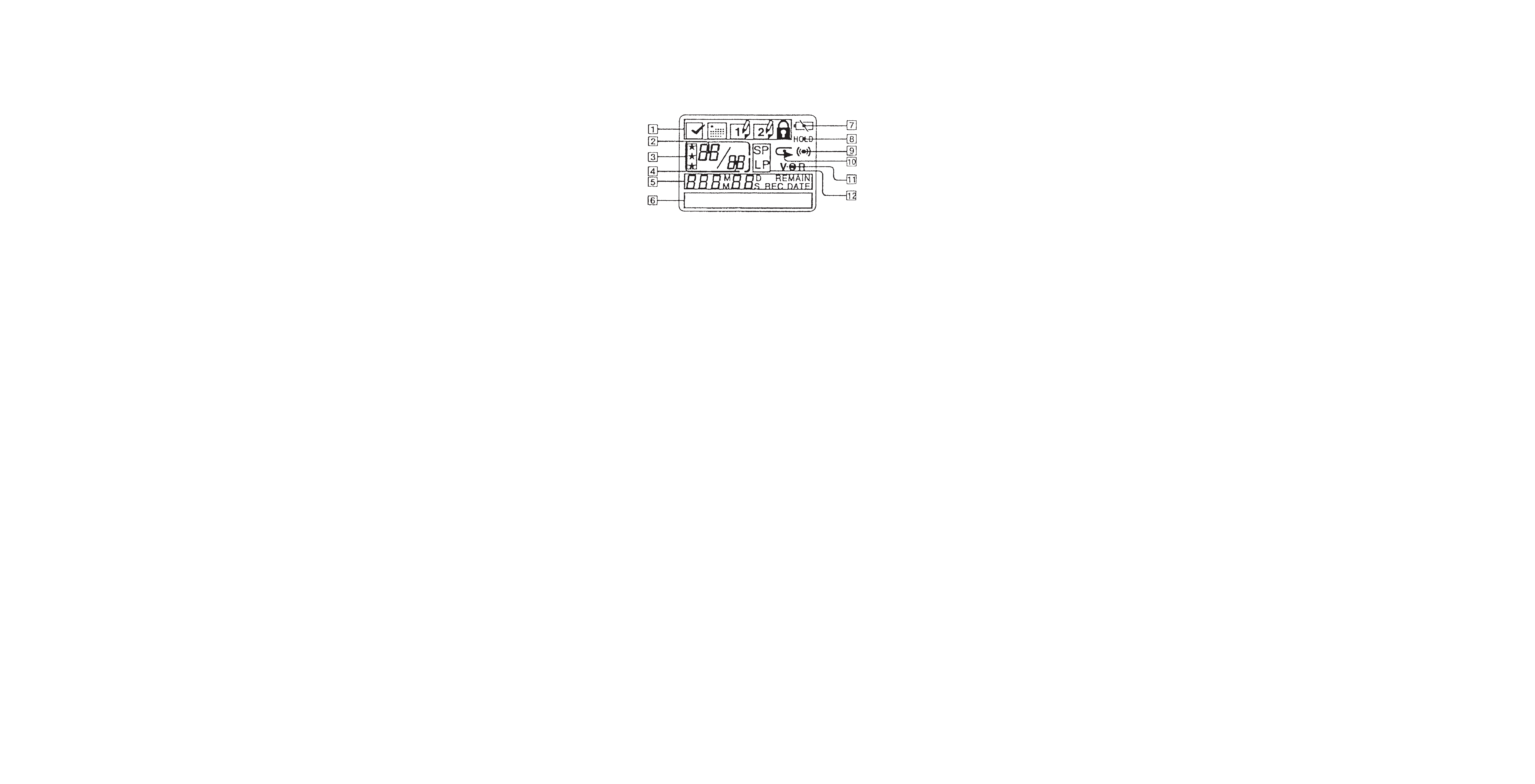
DISPLAY WINDOW
1 File icons
2 Current message number
3 Priority marks
4 Total number of messages in a file
5 REMAIN (Remaining recording time) indication
REC DATA (Recording data) indication
6 Current time/day indication
(15:30 TUE, etc)
Recording time indication
(10:10:10, etc)
Menu indication
(ALARM OFF, etc)
File name
(ACTION, SCHEDULE, etc)
Massages
(RECORD, ERASE?, etc)
7 Battery exhausted indicator
8 HOLD indicator
9 Alarm indicator
!º Repeat play indicator
!¡ Digital VOR indicator
!TM Recording mode indication
ICD-70
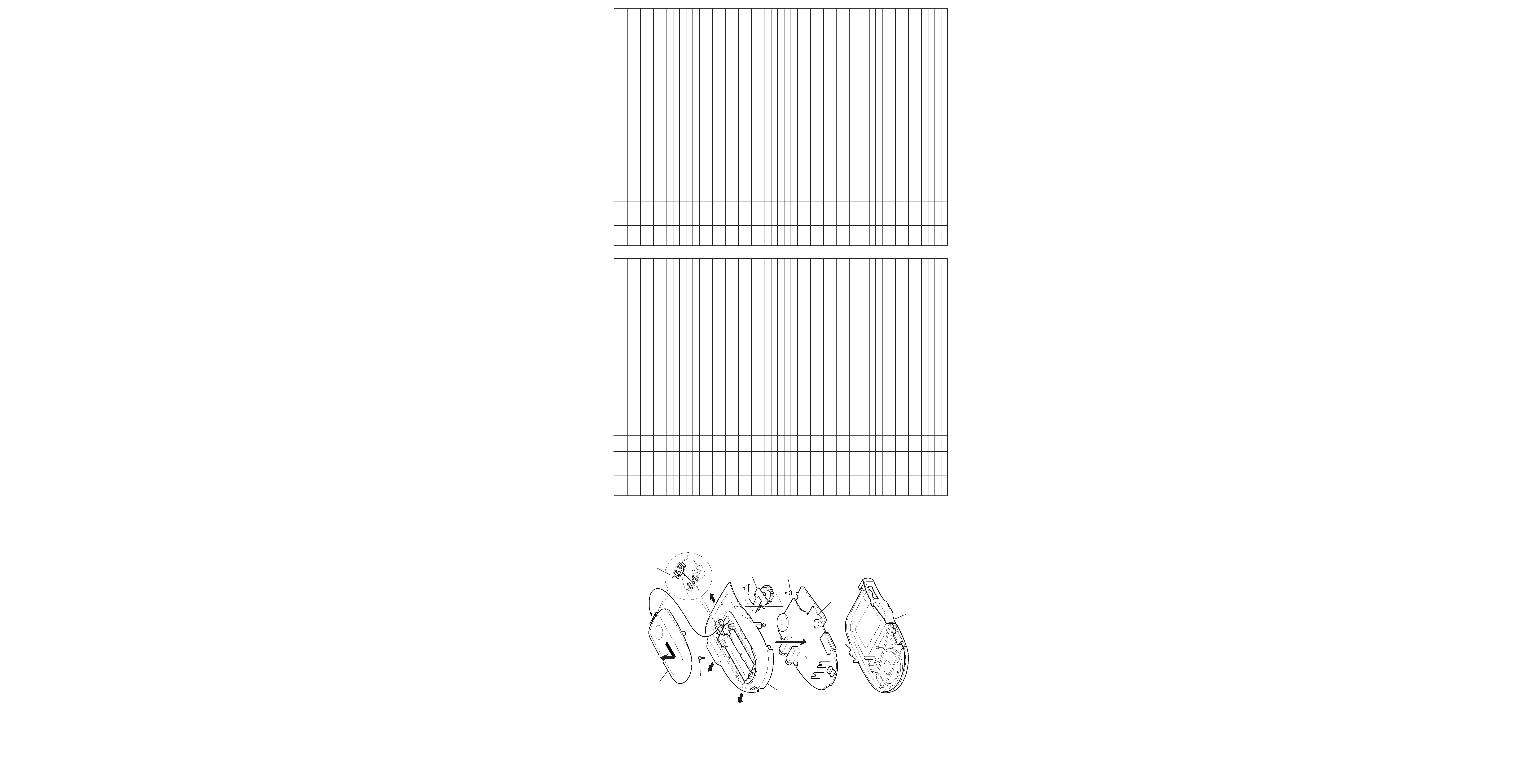
SECTION 2
DISASSEMBLY
1 Battery case lid
After pulling the Battery case lid to
the front as shown by arrow A ,
then remove it up wards.
2 Tapping screw (B1.7)
7 Case block assy
6 Switch unit
5 Two screws (1.7
× 2.5)
4 MAIN board
3 Upper lid assy
A
Note : Follow the disassembly procedure in the numerical order given.
SECTION 3
DIAGRAMS
3-1.
IC PIN FUNCTION
· IC701 MN102LP25Z3V
Pin No.
1
2
3
4
5
6
7
8
9
10
11
12
13
14
15
16
17
18
19
20
21
22
23
24
25
26
27
28
29
30
31
32
33
34
35
36
37
38
39
40
41
42
43
44
45
46
47
48
49
50
I/O
O
O
O
O
O
I
I
I
I
I
O
O
O
O
O
I
O
I
I
O
I
I
O
I
O
O
O
O
O
O
O
O
I
O
O
O
I
I
I
I
I
I
O
O
O
O
I
O
I
Description
"Speaker amplifier, mute control."
PDN (Power Down) output to IC101.
RES (Reset) output to IC101.
"Microphone sensitivity selection output (0: Low, 1: High)."
CE (Chip Enable) output to IC702.
R/B (Ready/Busy) input from IC702.
ERASE switch input detection.
HOLD switch input detection.
"Input audio present/absent detect signal input from IC104. (0: Sound is present, 1: No sound)."
Backup power supply voltage detection input from IC503.
IC101 analog signal output mute control.
B+ power supply control output.
Backup power supply connection (charge) control.
IC501 regulator control (ON/OFF) output.
IC504 DC/DC converter ON/OFF control output.
Power supply (+).
System clock output.
GND.
Subsystem clock (32 kHz).
Subsystem clock (32 kHz).
Power supply (+).
Main system clock (10 MHz).
Main system clock (10 MHz).
"Single chip mode setting terminal (Fixed to "1" always).
OPR LED (red) driving terminal (REC).
OPR LED (green) driving terminal (PLAY).
Not used. Fixed to Low output.
Not used. Fixed to Low output.
LCD back-light control.
Wav Link ACK output.
Wav Link OPT output.
Wav Link WLOK output.
Power supply (+).
Not used. Fixed to Low output.
Not used. Fixed to Low output.
Not used. Fixed to Low output.
"Wav Link WLINK input. (Low: during link, High: no connection)."
Wav Link COM0 input.
Wav Link COM1 input.
Wav Link COM2 input.
Wav Link COM3 input.
GND.
DAT output to IC106.
CLK output to IC106.
LE output to IC106.
Not used. Fixed to Low output.
Test mode signal input.
Not used. Fixed to Low output.
Wav Link C/D input. (Command/Data identification).
Pin Name
PO_PMUT
--
POA_PDN
POA_RES
PO_MIC
POR_CE
PIR_PB
PI_ERS
PI_HOLD
PI_VOR
PI_DET3
PO_MUTE
PO_BOT
PO_BACK
PO_REGU
PO_DDC
VDD
SYSCLK
VSS
XI
XO
VDD
OSCI
OSCO
MODE
POL_REC
POL_PLY
--
--
PO_LIGH
PO_ACK
PO_OPT
PO_WLOK
VDD
--
--
--
PI_WLNK
PI_COM0
PI_COM1
PI_COM2
PI_COM3
VSS
POS_DAT
POS_CLK
POS_LE
PI_CHKO
PI_TEST
--
PI_C_D
Pin No.
51
52
53
54
55
56
57
58
59
60
61
62
63
64
65
66
67
68
69
70
71
72
73
74
75
76
77
78
79
80
81
82
83
84
85
86
87
88
89
90
91
92
93
94
95
96
97
98
99
100
I/O
O
O
O
I
O
O
O
O
O
O
I
I
I
O
O
I
O
I
O
O
O
O
I
I
I
I
I
I
I
I
I
I
I
I/O
I/O
I/O
I/O
I/O
I/O
I/O
I/O
I
O
O
O
O
O
O
O
Description
Power down control output to IC105.
Vref control output to LCD driver.
Beep waveform output.
Power supply (+).
Not used. Fixed to Low output.
"Power supply lid OPEN detect control (H: detection enable, L: detection disable)"
Selection of clock to be supplied to MCK (10 MHz).
Selection of clock to be supplied to MCK (7 MHz).
Key Vcc control.
"LCD driver, Vdd control."
GND.
Battery voltage detection.
Key voltage detection.
Not used. Fixed to Low output.
CLR output to IC107 (Startup of XSYNC signal).
Power supply (+).
CLR output to IC101 (Serial send/receive clock output).
IS input from IC101 (Serial data input).
IR output to IC101 (Serial data output).
SCK output to LCD driver (Serial receive clock output).
STB output to LCD driver.
DAT output to LCD driver (Serial data output).
Non-maskable interrupt input/output terminal.
Serial send/receive with IC101 start signal input.
WAV Link REQ interrupt input.
"Interrupt caused by key operation, processing start signal input."
"Interrupt caused by battery lid switch operation, processing start signal input."
"Interrupt caused by JOG rotation, processing start signal input."
"Interrupt caused by JOG rotation B-phase signal input, processing start signal input."
Microprocessor reset terminal.
Power supply (+).
Data I/O with IC702 (flash memory).
Data I/O with IC702 (flash memory).
Data I/O with IC702 (flash memory).
Data I/O with IC702 (flash memory).
Data I/O with IC702 (flash memory).
Data I/O with IC702 (flash memory).
Data I/O with IC702 (flash memory).
Data I/O with IC702 (flash memory).
GND.
CLE output to IC702 (flash memory).
ALE output to IC702 (flash memory).
WE output to IC702 (flash memory).
RE output to IC702 (flash memory).
Not used. Fixed to Low output.
SE output to IC702.
WP output to IC702.
Not used. Fixed to Low output.
Pin Name
PO_PAMP
PO_LCDR
PO_BEEP
VDD
--
PO_BOP
PO_SPC
PO_LPC
PO_KEYV
PO_LCDV
VSS
batt A/D
key A/D
--
PO_CHK1
VDD (VPP)
POA_CLK
PIA_IS
POA_IR
POD_SCK
POD_STB
POD_DAT
PULL UP
PULL UP
NMI
XSYNC
PI_REQ
PI_WAKE
PI_OPEN
PI_ROTA
PI_ROTB
RST
VDD
POO
PO1
PO2
PO3
PO4
PO5
PO6
PO7
VSS
POR_CLE
POR_ALE
POR_WE
RE
--
SE
WP
--
-- 5 --
-- 6 --
-- 7 --
2-1.
BATTERY CASE LID, MAIN board