HCD-VX550
Chinese Model
SERVICE MANUAL
MINI Hi-Fi COMPONENT SYSTEM
MICROFILM
HCD-VX550 is the Amplifier, Video
CD player, Tape Deck and Tuner
section in MHC-VX550.
Continued on next page
SPECIFICATIONS
Dolby noise reduction manufactured under license
from Dolby Laboratories Licensing Corporation.
"DOLBY" and the double-D symbol
a are trade-
marks of Dolby Laboratories Licensing Corporation.
Model Name Using Similar Mechanism
NEW
CD Mechanism Type
CDM38LH-5BD36L
Base Unit Name
BU-26BD36L
Optical Pick-up Name
KSS-213D/Q-RP
Model Name Using Similar Mechanism
HTC-V5550
Tape Transport Mechanism Type
TCM-230AWR2
CD
Section
Tape deck
Section
Amplifier section
The following measured at AC 120, 220, 240 V 50/60
Hz
DIN power output (rated)110 + 110 W
(8
at 1 kHz, DIN)
Continuous RMS power output (reference)
140 + 140 W
(8
at 1 kHz, 10% THD)
Inputs
MD IN:
voltage 450 mV,
(phono jacks)
impedance 47 k
VIDEO (AUDIO) IN:
voltage 250 mV,
(phono jacks)
impedance 47 k
MIC 1/2 (phone jack):
sensitivity 1 mV, impedance
10 k
Outputs
MD OUT (phono jacks): voltage 250 mV
impedance 1 k
VIDEO OUT (phono jack):
max,output level
1Vp-p, unbalanced, Sync
negative, load impedance
75
S-VIDEO OUT (4-pin/ mini-DIN jack):
Y: 1Vp-p, unbalanced,
Sync negative,
C: 0.286Vp-p,
load impedance 75
PHONES (stereo phone jack):
accepts headphones of 8
or more
SPEAKER:
accepts impedance of 8 to
16
SUPER WOOFER
Voltage 1 V, impedance
1
k
SUPER VIDEO CD/VIDEO CD
/CD player section
System
Compact disc and digital
audio and video system
Laser
Semiconductor laser
(
=780nm)
Emission duration:
continuous
Laser output
Max. 44.6 µW*
*This output is the value
measured at distance of 200
mm from the objective lens
surface on the Optical Pick-up
Block with 7 mm aperture.
Frequency response
2 Hz - 20 kHz (±0.5 dB)
Wavelength
780 -790 nm
Signal-to-noise ratio
More than 90 dB
Dynamic range
More than 90 dB
Video color system format
NTSC, PAL

2
CD OPTICAL DIGITAL OUT
(Square optical connector jack, rear panel)
Wavelength
660 nm
Output Level
18 dBm
Tape player section
Recording system
4-track 2-channel stereo
Frequency response
40 - 13,000 Hz (±3 dB),
(DOLBY NR OFF)
using Sony TYPE I cassette
40-14,000 Hz (± 3 dB),
using Sony TYPE II cassette
Tuner section
Fm stereo, FM/ AM superheterodyne tuner
FM tuner section
Tuning range
87.5-108.0 MHz
Antenna
FM lead antenna
Antenna terminals
75
unbalanced
Intermediate frequency 10.7 MHz
AM tuner section
Tuning range
2 Band type:
531-1,602 kHz
(with the interval set at 9 kHz)
530-1,710 kHz
(with the interval set at 10 kHz)
3 Band type:
MW:
531-1,602 kHz
(with the interval set at 9 kHz)
530-1,710 kHz
(with the interval set at 10 kHz)
SW:
5.95-17.90 MHz
(with the interval set at 5 kHz)
Antenna
AM loop antenna
Antenna terminals
External antenna terminal
Intermediate frequency 450 kHz
General
Power requirements
220 V AC, 50/ 60 Hz
Power consumption:
160 W
Dimensions (w/h/d)
Approx. 280
× 340 × 395 mm
Mass:
Approx. 10.0 kg
Design and specifications are subject to change without notice.
TABLE OF CONTENTS
1. SERVICING NOTES ················································· 3
2. GENERAL .......................................................................... 5
3. DISASSEMBLY ................................................................ 8
4. TEST MODE ................................................................... 11
5. MECHANICAL ADJUSTMENTS ............................ 14
6. ELECTRICAL ADJUSTMENTS
DECK Section .................................................................. 14
CD Section ....................................................................... 17
VIDEO Section ................................................................. 17
7. DIAGRAMS
7-1.
Block Diagram
CD SERVO Section .......................................................... 18
AUDIO/VIDEO CD Section ............................................ 19
TAPE DECK Section ....................................................... 20
MAIN Section .................................................................. 21
DISPLAY/KEY CONTROL/
POWER SUPPLY Section ················································ 22
7-2.
Circuit Board Location ····················································· 23
7-3.
Printed Wiring Board BD Board .................................... 24
7-4.
Schematic Diagram BD Board ....................................... 25
7-5.
Schematic Diagram VIDEO Board (1/2) ........................ 26
7-6.
Schematic Diagram VIDEO Board (2/2) ........................ 27
7-7.
Printed Wiring Board VIDEO Board .............................. 28
7-8.
Printed Wiring Boards CD MOTOR Section ................. 30
7-9.
Schematic Diagram CD MOTOR Section ...................... 31
7-10. Printed Wiring Board AUDIO Board ............................. 32
7-11. Schematic Diagram AUDIO Board ................................ 33
7-12. Printed Wiring Board LEAF SW Board ......................... 34
7-13. Schematic Diagram LEAF SW Board ............................ 34
7-14. Printed Wiring Board MAIN Board ............................... 35
7-15. Schematic Diagram MAIN Board (1/4) ......................... 36
7-16. Schematic Diagram MAIN Board (2/4) ......................... 37
7-17. Schematic Diagram MAIN Board (3/4) ......................... 38
7-18. Schematic Diagram MAIN Board (4/4) ......................... 39
7-19. Printed Wiring Board PANEL Board ............................. 40
7-20. Schematic Diagram PANEL Board ................................ 41
7-21. Printed Wiring Board CD SW/5V POWER Board ........ 42
7-22. Schematic Diagram CD SW/5V POWER Board ........... 42
7-23. Printed Wiring Board TRANSFORMER Board ............ 43
7-24. Schematic Diagram TRANSFORMER Board ............... 43
7-25. Printed Wiring Board SURROUND Board .................... 44
7-26. Schematic Diagram SURROUND Board ....................... 44
7-27. IC Block Diagrams ........................................................... 45
7-28. IC Pin Function Description ............................................. 49
8. EXPLODED VIEWS ..................................................... 60
9. ELECTRICAL PARTS LIST ..................................... 68
3
SECTION 1
SERVICING NOTES
SELF-DIAGNOSIS
This unit is equipped with a self-diagnosis function.
The function is used for diagnosing the conditions of the circuits of
the VIDEO board.
The circuits can be determined if normal or abnormal by the lighting
of D502 of the VIDEO board.
Lighting of D502
When lit
: Operates normally
Blinks repeatedly : The circuit may be faulty.
VIDEO Board (SIDE B)
The laser diode in the optical pick-up block may suffer electrostatic
break-down because of the potential difference generated by the
charged electrostatic load, etc. on clothing and the human body.
During repair, pay attention to electrostatic break-down and also
use the procedure in the printed matter which is included in the
repair parts.
The flexible board is easily damaged and should be handled with
care.
NOTES ON LASER DIODE EMISSION CHECK
The laser beam on this model is concentrated so as to be focused on
the disc reflective surface by the objective lens in the optical pick-
up block. Therefore, when checking the laser diode emission,
observe from more than 30 cm away from the objective lens.
Notes on chip component replacement
· Never reuse a disconnected chip component.
· Notice that the minus side of a tantalum capacitor may be dam-
aged by heat.
Flexible Circuit Board Repairing
· Keep the temperature of the soldering iron around 270 °C dur-
ing repairing.
· Do not touch the soldering iron on the same conductor of the
circuit board (within 3 times).
· Be careful not to apply force on the conductor when soldering
or unsoldering.
NOTES ON HANDLING THE OPTICAL PICK-UP
BLOCK OR BASE UNIT
CAUTION
Use of controls or adjustments or performance of procedures
other than those specified herein may result in hazardous
radiation exposure.
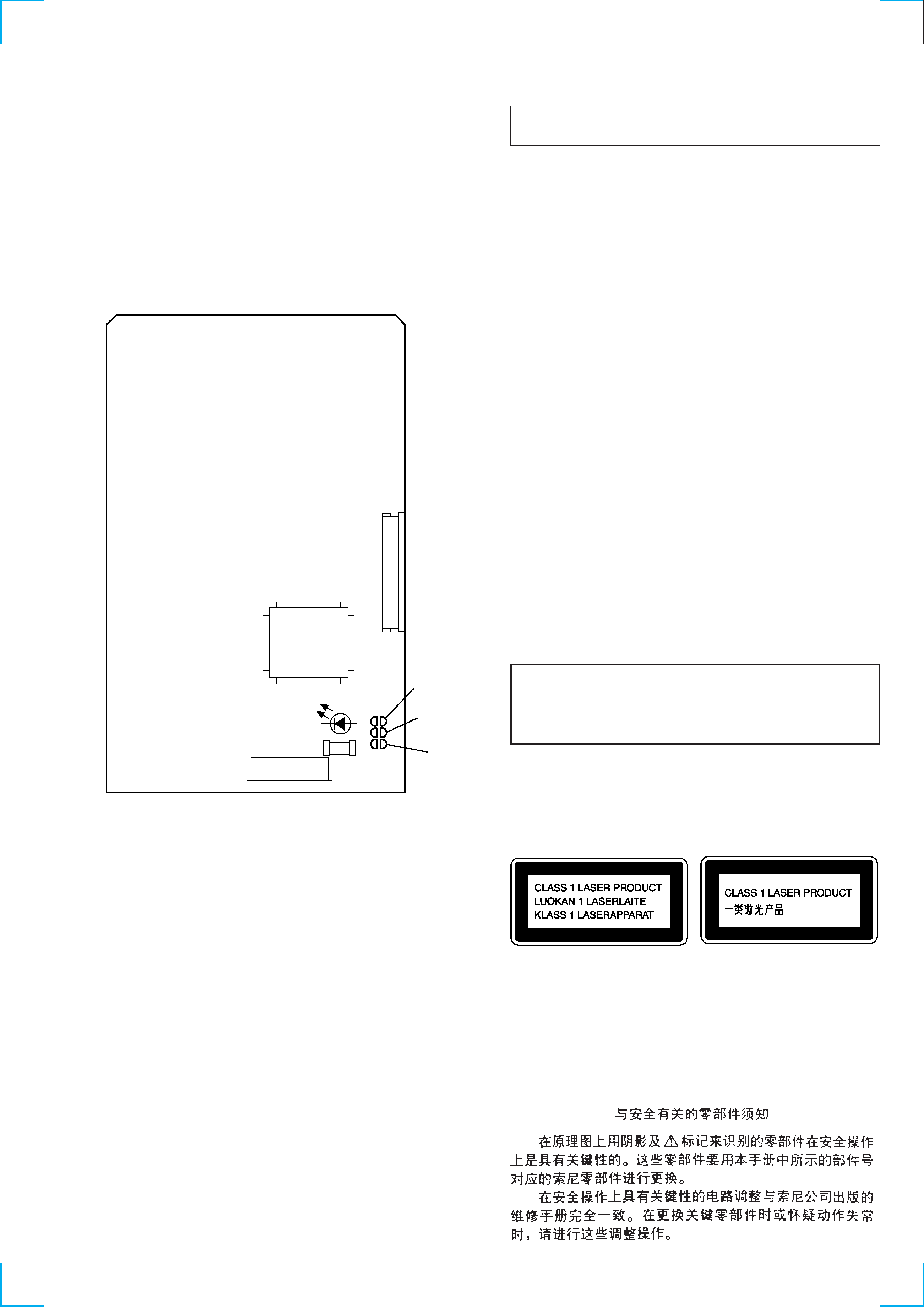
This appliance is classified as a CLASS 1 LASER product.
The CLASS 1 LASER PRODUCT MARKING is located on
the rear exterior.
Laser component in this product is capable of emitting radiation
exceeding the limit for Class 1.
SAFETY-RELATED COMPONENT WARNING!!
COMPONENTS IDENTIFIED BY MARK
! OR DOTTED LINE WITH
MARK
! ON THE SCHEMATIC DIAGRAMS AND IN THE PARTS
LIST ARE CRITICAL TO SAFE OPERATION. REPLACE THESE
COMPONENTS WITH SONY PARTS WHOSE PART NUMBERS
APPEAR AS SHOWN IN THIS MANUAL OR IN SUPPLEMENTS
PUBLISHED BY SONY.
IC505
CN501
CN502
SL501
SL503
100
81
1
30
31
50
51
80
SL502
D502
4
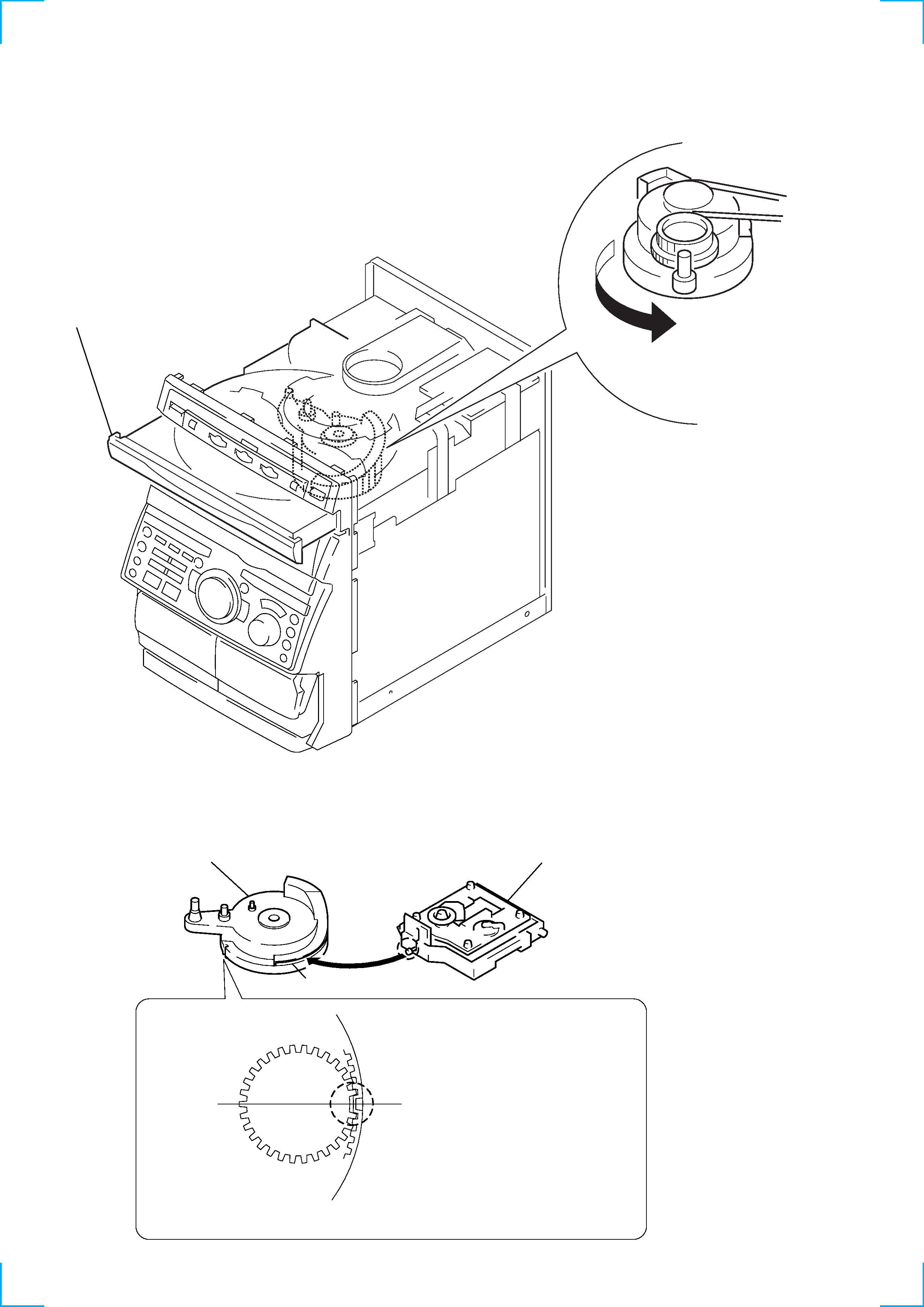
NOTE FOR INSTALLATION (ROTARY ENCODER)
HOW TO OPEN THE DISC TRAY WHEN POWER SWITCH TURNS' OFF.
1 Remove the Case.
3 Pull-out the disc tray.
2 Turn the cam to the
direction of arrow.
BU cam
Groove
Section A
Note:When attaching the Base unit, Insert the
section A into the groove of BU cam.
Note:When attaching the BU cam,
engage the Rotary encoder
switch as shown in the figure.
5
SECTION 2
GENERAL
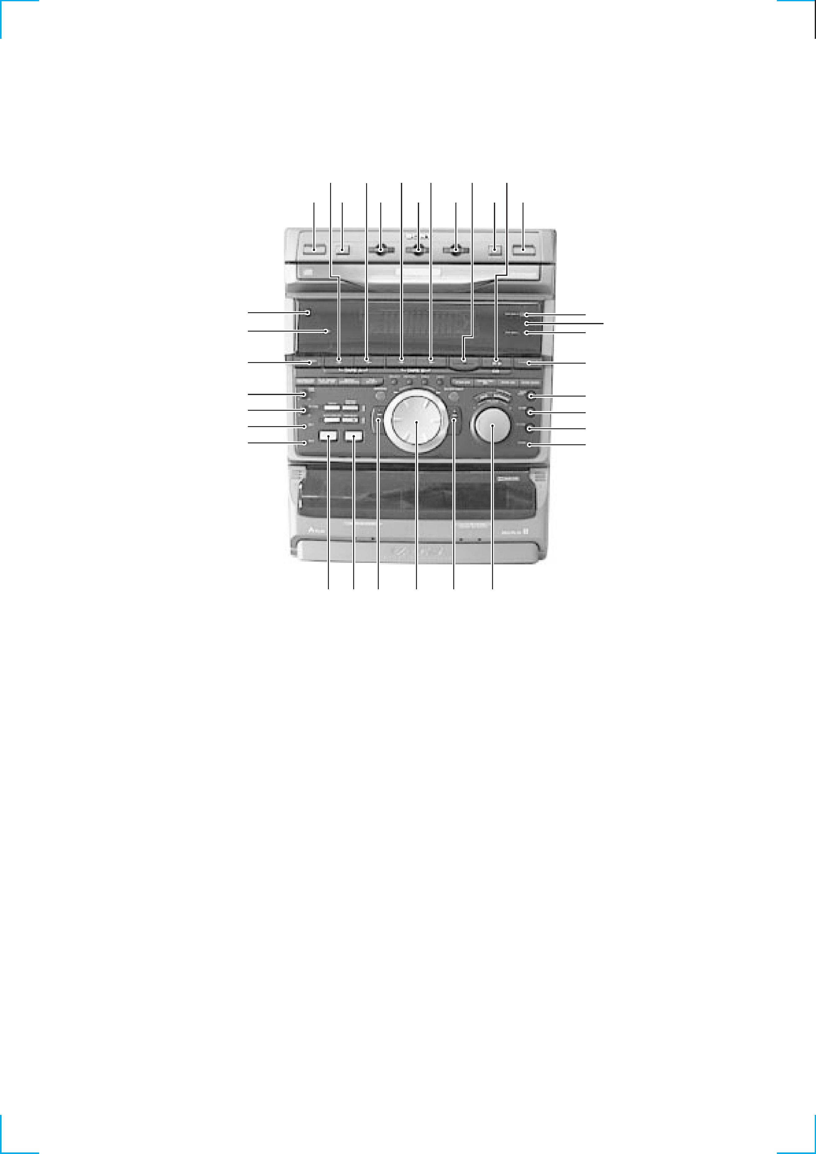
· LOCATION OF CONTENTS
Front View
1
1/u button
2
9 TAPE A button and indicator
3
(STANDBY) DEMO button
4
( TAPE A button and indicator
5
DISC 1 button
6
9 TAPE B button and indicator
7
DISC 2 button
8
( TAPE B button and indicator
9
DISC 3 button
0
p button
qa
DISC SKIP, EX-CHANGE button
qs
^ CD button and indicator
qd
§ button
qf
SVCD/VCD indicator
qg
PBC indicator
qh
PBC OFF indicator
qj
TUNER/BAND button
13
5
7
9
qa
qs
0
8
6
4
2
qd
qf
qh
qj
qk
ql
w;
wa
ws
wd
wf
wg
wh
wj
wk
wl
e;
ea
es
ed
ef
qg
qk
REC PAUSE/START button and indicator
ql
HI-DUB button
w;
CD SYNC button
wa
PHONE jack
ws
VOLUME knob
wd
+
) button and indicator
wf
JOG dial and indicator
wg
0 button and indicator
wh
CD FLASH button
wj
CD LOOP button
wk
MIC 2 jack
wl
MIC 1 jack
e;
MIC LEVEL knob
ea
ECHO LEVEL knob
es
FUNCTION button
ed
SYNC EQ indicator
ef
EFFECT indicator