1
MICROFILM
HCD-SD1
SPECIFICATIONS
SERVICE MANUAL
COMPACT DISC RECEIVER
-- Continued on next page --
AEP Model
UK Model
E Model
HCD-SD1 is the amplifier, CD and
tuner section in CMT-SD1.
Model Name Using Similar Mechanism
HCD-MD313
Mechanism Type
CDM13B-5BD19
Base Unit Type
BU-5BD19
Optical Pick-up Type
KSS-213B/K-N
CD
SECTION
2
CAUTION
Use of controls or adjustments or performance of procedures
other than those specified herein may result in hazardous ra-
diation exposure.
Notes on chip component replacement
· Never reuse a disconnected chip component.
· Notice that the minus side of a tantalum capacitor may be
damaged by heat.
Flexible Circuit Board Repairing
· Keep the temperature of soldering iron around 270°C
during repairing.
· Do not touch the soldering iron on the same conductor of the
circuit board (within 3 times).
· Be careful not to apply force on the conductor when soldering
or unsoldering.
Laser component in this product is capable of emitting radiation
exceeding the limit for Class 1.
This appliance is classified as
a CLASS 1 LASER product.
The CLASS 1 LASER PROD-
UCT MARKING is located on
the rear exterior.
This caution
label is located
inside the unit.
SAFETY-RELATED COMPONENT WARNING !!
COMPONENTS IDENTIFIED BY MARK
! OR DOTTED LINE
WITH MARK
! ON THE SCHEMATIC DIAGRAMS AND IN
THE PARTS LIST ARE CRITICAL TO SAFE OPERATION.
REPLACE THESE COMPONENTS WITH SONY PARTS
WHOSE PART NUMBERS APPEAR AS SHOWN IN THIS
MANUAL OR IN SUPPLEMENTS PUBLISHED BY SONY.
PARTS No.
4-212-711-0
4-212-712-0
MODEL
AEP, UK model
SP, HK model
· Abbreviation
HK
: Hong Kong model
SP
: Singapore model
Parts No.
MODEL NO. HCD-SD1
MODEL IDENTIFICATION
Specification Label

3
TABLE OF CONTENTS
1. SERVICING NOTE .......................................................... 4
2. GENERAL .......................................................................... 7
3. DISASSEMBLY
3-1. Loading Panel ....................................................................... 8
3-2. Glass ASSY ........................................................................... 8
3-3. Front Panel ........................................................................... 9
3-4. Main Board and Tuner Unit .................................................. 9
3-5. CD Mechanism Deck .......................................................... 10
3-6. Back Panel ......................................................................... 10
3-7. Disc Table .......................................................................... 11
3-8. Optical Pick-up ................................................................... 11
4. SERVICE MODE ............................................................. 12
5. TEST MODE ..................................................................... 13
6. ELECTRICAL ADJUSTMENTS ............................... 14
7. DIAGRAMS
7-1. Circuit Boards Location ...................................................... 16
7-2. Block Diagrams
· BD Section ....................................................................... 17
· Main Section .................................................................... 19
7-3. Schematic Diagram BD Section ................................... 23
7-4. Printed Wiring Board BD Section ................................. 25
7-5. Schematic Diagram Main (1/2) Section ........................ 27
7-6. Schematic Diagram Main (2/2) Section ........................ 29
7-7. Printed Wiring Board Main Section .............................. 31
7-8. Schematic Diagram Sub Trans Section ......................... 33
7-9. Printed Wiring Board Sub Trans Section ...................... 34
7-10. Schematic Diagram Panel Section ............................. 35
7-11. Printed Wiring Board Panel Section ........................... 37
7-12. Schematic Diagram AMP Section .............................. 39
7-13. Printed Wiring Board AMP Section ........................... 41
7-14. Schematic Diagram Connector Section ...................... 43
7-15. Printed Wiring Board Connector Section ................... 45
7-16. Schematic Diagram REG Section .............................. 47
7-17. Printed Wiring Board REG Section ............................ 49
7-18. IC Block Diagrams ........................................................... 51
7-19. IC Pin Functions ............................................................... 54
8. EXPLODED VIEWS
8-1. Front Panel Section ............................................................. 56
8-2. Chassis Section ................................................................... 57
8-3. Mechanism Deck Section (CDM13B-5BD19) ................... 58
8-4. Base Unit Section (BU-5BD19) .......................................... 59
9. ELECTRICAL PARTS LIST ........................................ 60
NOTES ON HANDLING THE OPTICAL PICK-UP BLOCK
OR BASE UNIT
The laser diode in the optical pick-up block may suffer electrostatic
break-down because of the potential difference generated by the
charged electrostatic load, etc. on clothing and the human body.
During repair, pay attention to electrostatic break-down and also
use the procedure in the printed matter which is included in the
repair parts.
The flexible board is easily damaged and should be handled with
care.
NOTES ON LASER DIODE EMISSION CHECK
The laser beam on this model is concentrated so as to be focused on
the disc reflective surface by the objective lens in the optical pick-
up block. Therefore, when checking the laser diode emission, ob-
serve from more than 30 cm away from the objective lens.
LASER DIODE AND FOCUS SEARCH OPERATION
CHECK
Carry out the "S curve check" in "CD section adjustment" and check
that the S curve waveform is output two times.
4
SECTION 1
SERVICING NOTE
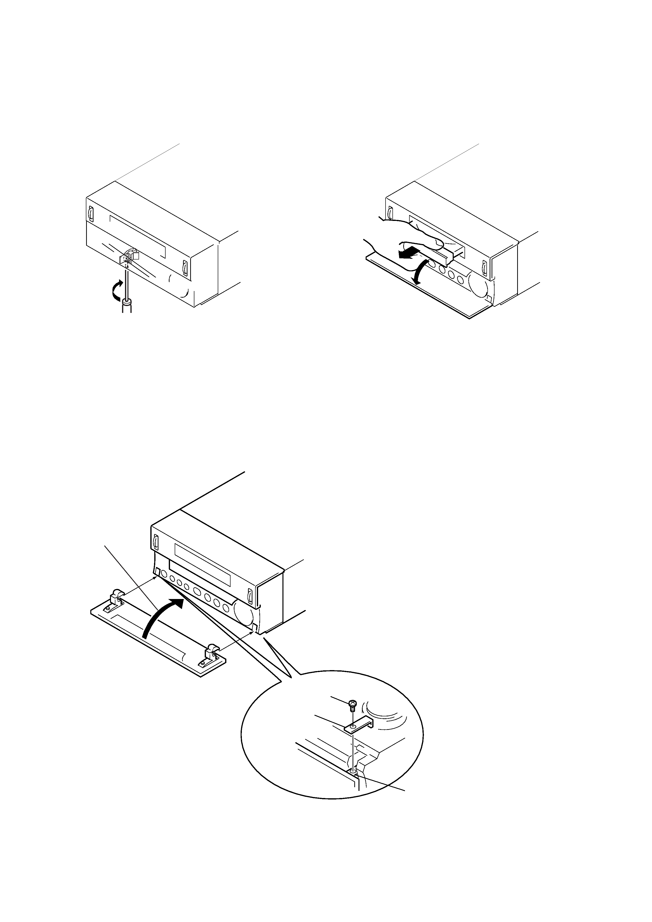
OPENING THE DISC TRAY WHEN POWER IS OFF
1 Using a thin screwdriver, rotate the internal cam
in the arrow direction completely.
2 Open the glass door, and pull out the loading panel.
1
2 Pull up the glass door,
in the arrow direction.
4 Screw (PTP 2.6x6)
3 Bracket (shaft)
(Bottom side)
1
When securing this part, position at the
center to allow some play. Open and close
the glass window several times, and check
that the parts do not touch each other.
ATTACHING THE GLASS ASSEMBLY
· Attach according to steps 1 to 4.
5
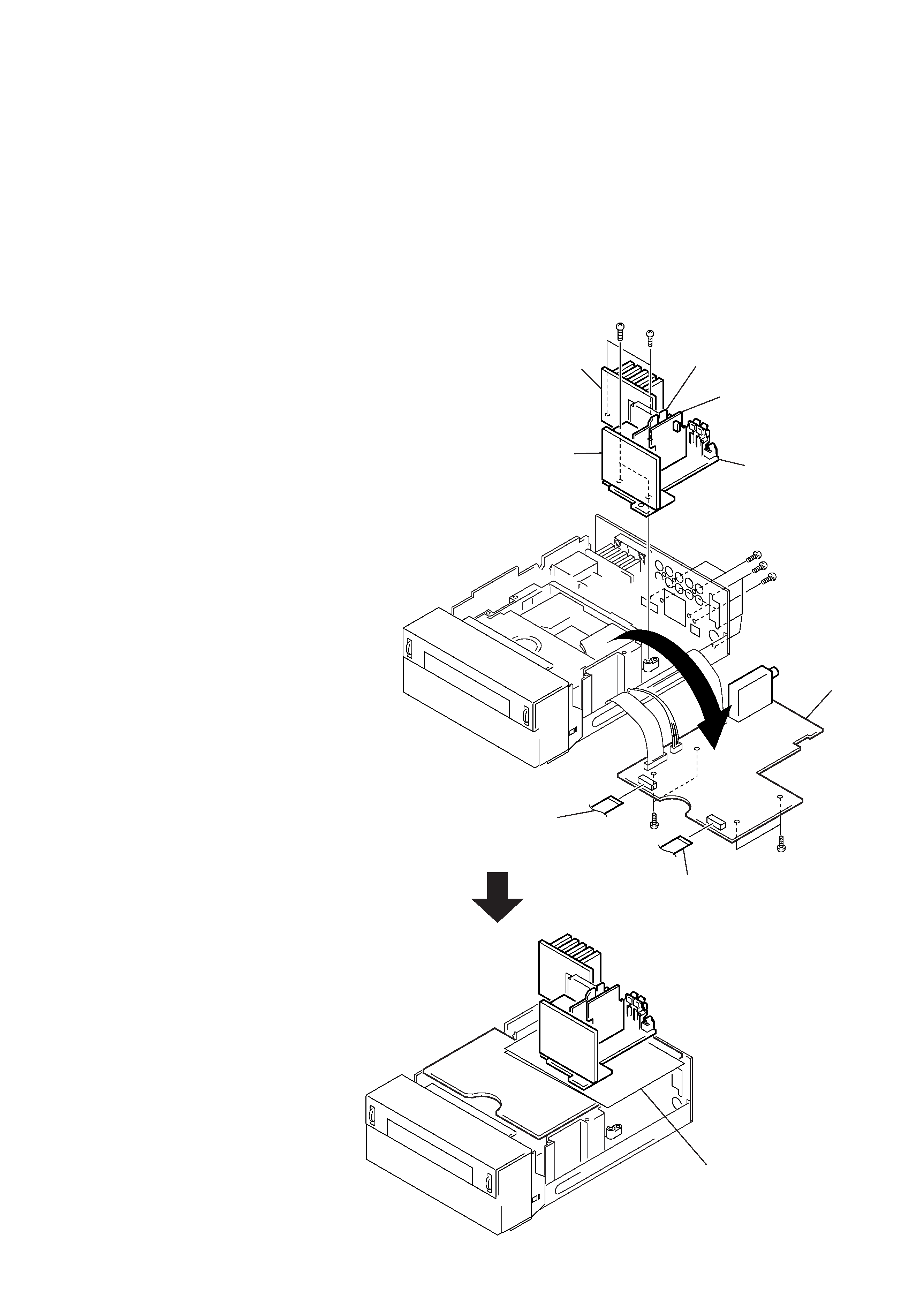
POSITIONS FOR SERVICING THE CONNECTOR
BOARD, SUB-TRANS BOARD, CHEMI-CON BOARD,
AND AMP BOARD
1 Remove the four screws securing the upper cover, and remove
the upper cover.
2 Remove the loading panel. (Refer to SECTION 3 DISASSEM-
BLY.)
3 Remove the four screws A securing the MAIN board, five screws
B securing the rear panel, two flat cables (CN701, CN702),
and open the MAIN board as shown in the figure.
4 Remove the two screws C securing the heat sink, and remove
the AMP board and CHEMI-CON board.
5 Remove the two screws D securing the SUB-TRANS board
and four screws E securing the CONNECTOR board, and re-
move the SUB-TRANS board and CONNECTOR board.
6 Return the MAIN board to its original position.
7 Insulate these boards and the MAIN board with paper, etc., and
assemble the CONNECTOR board, SUB-TRANS board,
CHEMI-CON board, and AMP board on these boards.
Should be insulatable
with paper, etc.
A
A
C
D
B
B
E
Heat sink
SUB-TRANS board
AMP board
CHEMI-CON board
CONNECTOR board
MAIN board
Flat type wire (CN701)
Flat type wire (CN702)