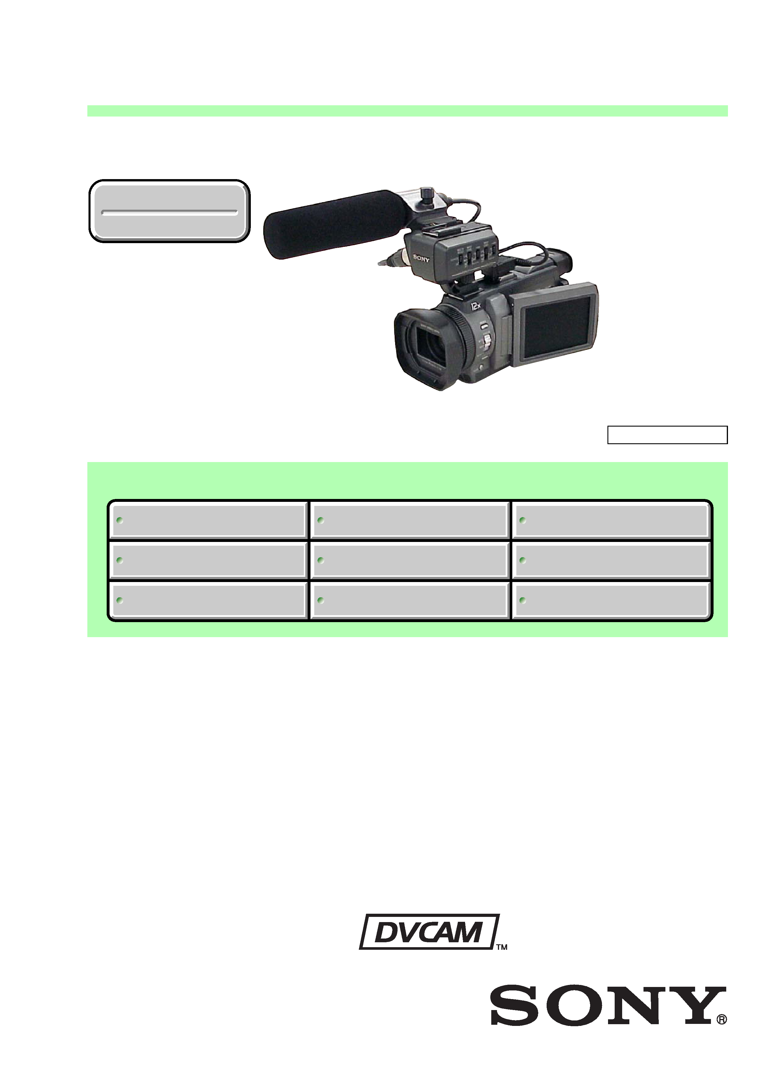
DSR-PDX10/PDX10P
RMT-811
US Model
Canadian Model
DSR-PDX10
AEP Model
UK Model
E Model
DSR-PDX10P
SERVICE MANUAL
DIGITAL CAMCORDER
J MECHANISM
· INSTRUCTION MANUAL is shown at the end of this document.
Link
SERVICE NOTE
DISASSEMBLY
BLOCK DIAGRAMS
FRAME SCHEMATIC DIAGRAMS
SCHEMATIC DIAGRAMS
PRINTED WIRING BOARDS
ADJUSTMENTS
REPAIR PARTS LIST
SPECIFICATIONS
SERVICE NOTE
DISASSEMBLY
BLOCK DIAGRAMS
FRAME SCHEMATIC DIAGRAMS
SCHEMATIC DIAGRAMS
PRINTED WIRING BOARDS
ADJUSTMENTS
REPAIR PARTS LIST
SPECIFICATIONS
Link
Revision History
Revision History
Ver 1.8 2005. 11

-- 2 --
DSR-PDX10/PDX10P
SPECIFICATIONS
SAFETY-RELATED COMPONENT WARNING!!
COMPONENTS IDENTIFIED BY MARK 0 OR DOTTED LINE WITH
MARK 0 ON THE SCHEMATIC DIAGRAMS AND IN THE PARTS
LIST ARE CRITICAL TO SAFE OPERATION. REPLACE THESE
COMPONENTS WITH SONY PARTS WHOSE PART NUMBERS
APPEAR AS SHOWN IN THIS MANUAL OR IN SUPPLEMENTS
PUBLISHED BY SONY.
ATTENTION AU COMPOSANT AYANT RAPPORT
À LA SÉCURITÉ!
LES COMPOSANTS IDENTIFÉS PAR UNE MARQUE 0 SUR LES
DIAGRAMMES SCHÉMATIQUES ET LA LISTE DES PIÈCES SONT
CRITIQUES POUR LA SÉCURITÉ DE FONCTIONNEMENT. NE
REMPLACER CES COMPOSANTS QUE PAR DES PIÈSES SONY
DONT LES NUMÉROS SONT DONNÉS DANS CE MANUEL OU
DANS LES SUPPÉMENTS PUBLIÉS PAR SONY.
COVER
COVER
CAUTION :
Danger of explosion if battery is incorrectly replaced.
Replace only with the same or equivalent type.
Video camera
recorder
System
Video recording system
2 rotary heads
Helical scanning system
Audio recording system
Rotary heads, PCM system
Quantization: Fs 32 kHz (12 bits,
channels 1/2, channels 3/4), Fs 48
kHz (16 bits, channels 1/2)
Video signal
PAL colour, CCIR standards
DSR-PDX10:
NTSC color, EIA standards
DSR-PDX10P:
DSR-PDX10:
Chrominance signal: 0.286 Vp-p
75
(ohms), unbalanced
Usable cassette
Mini DVCAM cassette with the
mark printed
Mini DV cassette with the
mark printed
Tape speed
DVCAM format:
Approx. 28.218 mm/s
DV format SP mode:
Approx. 18.812 mm/s
Recording/playback time (using
cassette PDVM-40ME)
DVCAM format: 40 min.
DV format SP mode: 1 hour
Fastforward/rewind time (using
cassette PDVM-40ME)
When using the battery pack:
Approx. 2 min. and 30 seconds
When using the AC power
adaptor:
Approx. 1 min. and 45 seconds
Viewfinder
Electric viewfinder (B&W)
Image device
3.8 mm (1/4.7 type) 3 CCD
(Charge Coupled Device)
Gross: Approx. 1 070 000 pixels
Effective (still):
Approx. 1 000 000 pixels
Effective (moving):
Approx. 690 000 pixels
Lens
Combined power zoom lens
Filter diameter: 37 mm
(1 1/2 in)
12
× (Optical), 48× (Digital)
F 1.6 2.8
Focal length
3.6 43.2 mm (5/32 1 3/4 in.)
When converted to a 35 mm still
camera
In CAMERA
4:3 mode :
49 588 mm (1 15/16 23 1/4 in.)
16:9 mode :
41 492 mm (1 5/8 19 3/8 in.)
In MEMORY
41 492 mm (1 5/8 19 3/8 in.)
Colour temperature
Auto, nIndoor (3 200 K),
Outdoor (5 800 K),
Minimum illumination
7 lx (lux) (F 1.6)
Input/Output connectors
S video input/output
4-pin mini DIN
Luminance signal: 1 Vp-p,
75
(ohms), unbalanced
Chrominance signal: 0.3 Vp-p,
75
(ohms), unbalanced
Audio/Video input/output
AV MINI JACK, 1 Vp-p,
75
(ohms), unbalanced, sync
negative
327 mV, (at output impedance
more than 47 k
(kilohms))
Output impedance with less than
2.2 k
(kilohms)/Stereo minijack
(ø 3.5 mm)
Input impedance more than
47 k
(kilohms)
DV input/output
4-pin connector
Headphone jack
Stereo minijack (ø 3.5 mm)
LANC jack
Stereo mini-minijack (ø 2.5 mm)
USB jack
mini-B
MIC jack
Minijack, 0.388 mV low impedance
with 2.5 to 3.0 V DC, output
impedance 6.8 k
(kilohms) (ø 3.5
mm)
Stereo type
INPUT1/INPUT2 connectors
XLR 3-pin, female, 60 dBu:
3 kilohms, +4 dBu: 10 kilohms
(0 dBu = 0.775 Vrms)
LCD screen
Picture
8.8 cm (3.5 type)
72.2
× 50.4 mm (2 7/8 × 2 in.)
Total dot number
246 400 (1 120
× 220)
General
Peak inrush current
Hot switching inrush current,
measured in accordance with
European standard EN55103-1:
6.3 A (230 V)
Power requirements
7.2 V (battery pack)
8.4 V (AC power adaptor)
Average power consumption
(when using the battery pack)
During camera recording using
LCD
6.3 W
Viewfinder
5.0 W
Operating temperature
0
°C to 40°C (32°F to 104°F)
Storage temperature
20
°C to + 60°C
(4
°F to + 140°F)
Dimensions (Approx.)
93
× 99 × 202 mm
(3 3/4
× 4 × 8 in.) (w/h/d)
Mass (Approx.)
950 g (2 lb 1 oz)
main unit only
1.4 kg (3 lb)
including the battery pack
NP-FM50, the XLR adaptor, the
Microphone, cassette PDVM-
40ME, the lens cap and shoulder
strap
Supplied accessories
See page 3.
AC power adaptor
Power requirements
100 240 V AC, 50/60 Hz
Power consumption
23 W
Output voltage
DC OUT: 8.4 V, 1.5 A in the
operating mode
Operating temperature
0
°C to 40°C (32°F to 104°F)
Storage temperature
20
°C to + 60°C
(4
°F to + 140°F)
Dimensions (approx.)
125
39 62 mm
(5
× 1 9/16 × 2 1/2 in.) (w/h/d)
excluding projecting parts
Mass (approx.)
280 g (9.8 oz)
excluding mains lead
Battery pack
Maximum output voltage
DC 8.4 V
Output voltage
DC 7.2 V
Capacity
8.5 Wh (1 180 mAh)
Dimensions (approx.)
38.2
× 20.5 × 55.6 mm
(1 9/16
× 13/16 × 2 1/4 in.)
(w/h/d)
Mass (approx.)
76 g (2.7 oz)
Type
Lithium ion
"Memory Stick"
Memory
Flash memory
8MB: MSA-8A
Operating voltage
2.7 3.6 V
Power consumption
Approx. 45 mA in the operating
mode
Approx. 130
µA in the standby
mode
Dimensions (approx.)
50
× 2.8 × 21.5 mm
(2
× 1/8 × 7/8 in.) (w/h/d)
Mass (approx.)
4 g (0.14 oz)
Design and specifications are
subject to change without notice.
DSR-PDX10P:
-- 3 --
DSR-PDX10/PDX10P
1.
Check the area of your repair for unsoldered or poorly-soldered
connections. Check the entire board surface for solder splashes
and bridges.
2.
Check the interboard wiring to ensure that no wires are
"pinched" or contact high-wattage resistors.
3.
Look for unauthorized replacement parts, particularly
transistors, that were installed during a previous repair. Point
them out to the customer and recommend their replacement.
4.
Look for parts which, through functioning, show obvious signs
of deterioration. Point them out to the customer and
recommend their replacement.
5.
Check the B+ voltage to see it is at the values specified.
6.
Flexible Circuit Board Repairing
· Keep the temperature of the soldering iron around 270°C
during repairing.
· Do not touch the soldering iron on the same conductor of the
circuit board (within 3 times).
· Be careful not to apply force on the conductor when soldering
or unsoldering.
Unleaded solder
Boards requiring use of unleaded solder are printed with the lead-
free mark (LF) indicating the solder contains no lead.
(Caution: Some printed circuit boards may not come printed with
the lead free mark due to their particular size.)
: LEAD FREE MARK
Unleaded solder has the following characteristics.
· Unleaded solder melts at a temperature about 40°C higher than
ordinary solder.
Ordinary soldering irons can be used but the iron tip has to be
applied to the solder joint for a slightly longer time.
Soldering irons using a temperature regulator should be set to
about 350°C.
Caution: The printed pattern (copper foil) may peel away if the
heated tip is applied for too long, so be careful!
· Strong viscosity
Unleaded solder is more viscous (sticky, less prone to flow) than
ordinary solder so use caution not to let solder bridges occur such
as on IC pins, etc.
· Usable with ordinary solder
It is best to use only unleaded solder but unleaded solder may
also be added to ordinary solder.
SAFETY CHECK-OUT
After correcting the original service problem, perform the following
safety checks before releasing the set to the customer.
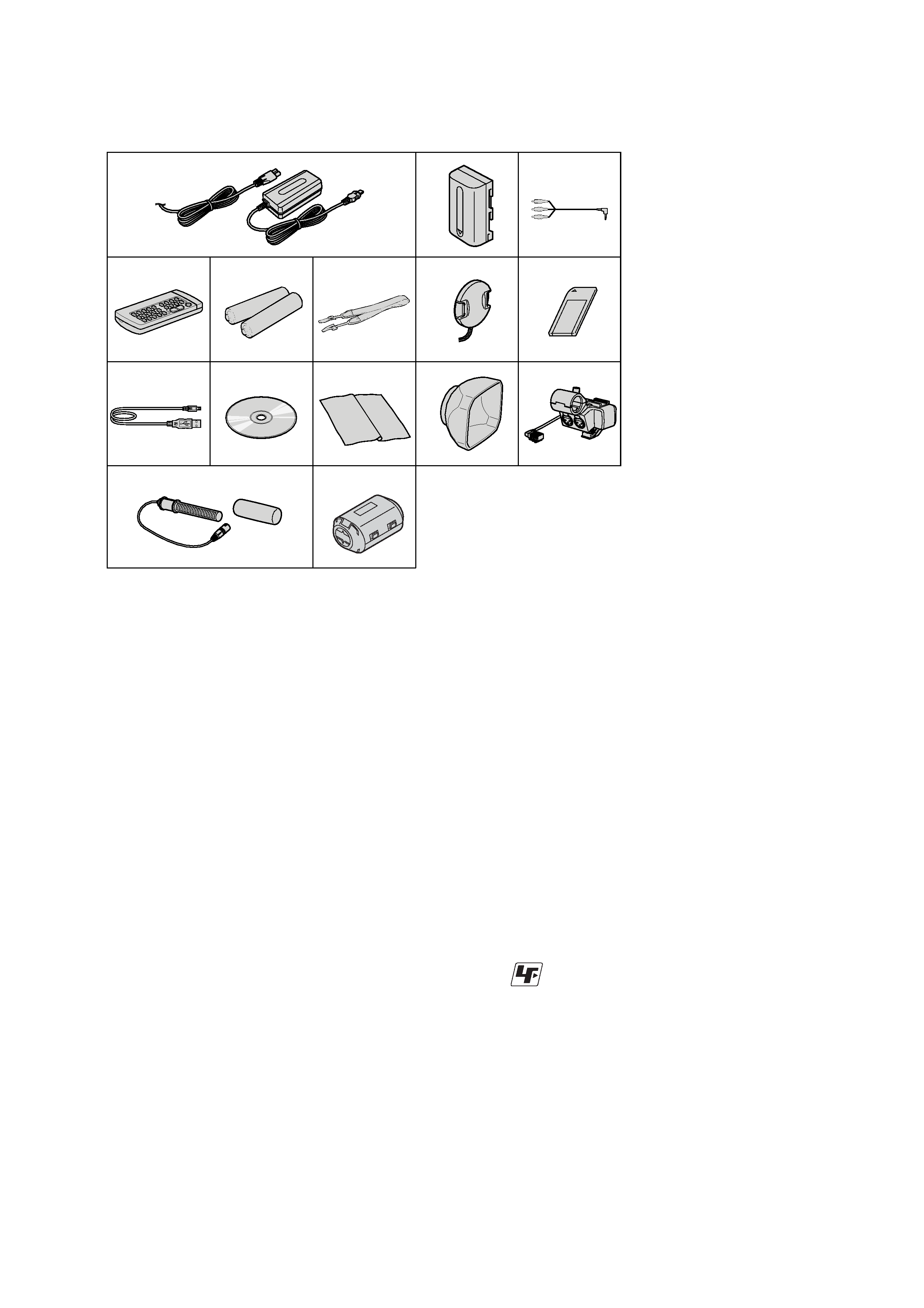
· SUPPLIED ACCESSORIES
Make sure that the following accessories are supplied with your camcorder.
9
1
4
q;
5
qa
qg
6
qs
2
7
3
8
qd
qf
1
AC-L10A/L10B/L10C AC power
adaptor (1), mains lead (1)
2
NP-FM50 battery pack (1)
3
A/V connecting cable (1)
4
Wireless Remote Commander (RMT-811)(1)
5
R6 (Size AA) battery for Remote Commander (2)
6
Shoulder strap (1)
7
Lens cap (1)
8
"Memory Stick" (1)
9
USB cable (1)
0
CD-ROM (SPVD-008 USB Driver) (1)(DSR-PDX10P)
CD-ROM (SPVD-008 (I) USB Driver) (1)(DSR-PDX10)
qa
Cleaning cloth (1)
qs
Wide lens hood (1)
qd
XLR adaptor (with a Microphone holder) (1)
qf
Microphone (1), Wind screen (1)
qg
Clamp filter (1)

-- 4 --
DSR-PDX10/PDX10P
TABLE OF CONTENTS
1.
SERVICE NOTE
1-1.
NOTE FOR REPAIR ····················································· 1-1
1-2.
POWER SUPPLY DURING REPAIRS ······················· 1-2
1-3.
TO TAKE OUT A CASSETTE WHEN NOT EJECT
(FORCE EJECT) ···························································· 1-2
1-4.
NOTES ON HANDLING THE LASER DIODE ······· 1-3
1-4-1. Soldering Conditions of Laser Unit (D501) ···················· 1-3
1-5.
SELF-DIAGNOSIS FUNCTION ··································· 1-4
1-5-1. Self-diagnosis Function ··················································· 1-4
1-5-2. Self-diagnosis Display ····················································· 1-4
1-5-3. Service Mode Display ····················································· 1-4
1-5-4. Self-diagnosis Code Table ··············································· 1-5
2.
DISASSEMBLY
2-1.
CABINET (R) BLOCK ··················································· 2-2
2-2.
P CABINET (C) ······························································ 2-2
2-3.
LCD MODULE ······························································· 2-3
2-4.
LCD BLOCK ·································································· 2-4
2-5.
FP-495 FLEXIBLE BOARD ·········································· 2-4
2-6.
CK-134 BOARD ····························································· 2-5
2-7.
F PANEL BLOCK ··························································· 2-5
2-8.
AF LASER BRACKET ASSEMBLY ····························· 2-6
2-9.
MA-425 BOARD ···························································· 2-7
2-10. FP-504 FLEXIBLE BOARD ·········································· 2-7
2-11. BATTERY PANEL BLOCK ··········································· 2-8
2-12. DB-016 BOARD ····························································· 2-8
2-13. MD BLOCK ···································································· 2-9
2-14. LENS BLOCK ······························································ 2-10
2-15. VC-318 BOARD ··························································· 2-10
2-16. MECHANISM DECK (J210) ······································· 2-11
2-17. EVF BLOCK ································································· 2-11
2-18. FP-497 FLEXIBLE BOARD ········································ 2-12
2-19. JK-222 BOARD ···························································· 2-12
2-20. CONTROL SWITCH BLOCK (PS-1870) ···················· 2-15
2-21. SE-132 BOARD ···························································· 2-15
2-22. GRIP CABINET BLOCK ············································· 2-16
2-23. CONTROL SWITCH BLOCK (CF-1870) ··················· 2-17
2-24. MS ASSEMBLY ··························································· 2-17
2-25. VF LENS ASSEMBLY ················································· 2-18
2-26. XLR BLOCK ································································ 2-19
2-27. XK-001 BOARD ··························································· 2-19
2-28. XM-002 BOARD, XD-002 BOARD, XS-002 BOARD ·· 2-20
2-29. CIRCUIT BOARDS LOCATION ································· 2-21
2-30. FLEXIBLE BOARDS LOCATION ······························ 2-22
3.
BLOCK DIAGRAMS
3-1.
OVERALL BLOCK DIAGRAM (1/5) ··························· 3-1
3-2.
OVERALL BLOCK DIAGRAM (2/5) ··························· 3-3
3-3.
OVERALL BLOCK DIAGRAM (3/5) ··························· 3-5
3-4.
OVERALL BLOCK DIAGRAM (4/5) ··························· 3-7
3-5.
OVERALL BLOCK DIAGRAM (5/5) ··························· 3-9
3-6.
POWER BLOCK DIAGRAM (1/3) ······························ 3-11
3-7.
POWER BLOCK DIAGRAM (2/3) ······························ 3-13
3-8.
POWER BLOCK DIAGRAM (3/3) ······························ 3-15
4.
PRINTED WIRING BOARDS AND
SCHEMATIC DIAGRAMS
4-1.
FRAME SCHEMATIC DIAGRAM (1/4) ······················· 4-1
FRAME SCHEMATIC DIAGRAM (2/4) ······················ 4-3
FRAME SCHEMATIC DIAGRAM (3/4) ······················· 4-5
FRAME SCHEMATIC DIAGRAM (4/4) ······················· 4-7
4-2.
SCHEMATIC DIAGRAMS
· CD-389 (CCD IMAGER)
SCHEMATIC DIAGRAM ··························· 4-11
· SE-132 (PITCH/YAW SENSOR)
SCHEMATIC DIAGRAM ···························· 4-13
· MA-425 (MIC AMP, AF LASER CONTROL)
SCHEMATIC DIAGRAM ···························· 4-15
· CK-134 (CONTROL SWITCH)
SCHEMATIC DIAGRAM ···························· 4-17
· JK-222 (AV IN/OUT, DV/USB CONNECTOR)
SCHEMATIC DIAGRAM ···························· 4-19
· PD-191 (1/2) (LCD DRIVER, TIMING GENERATOR)
SCHEMATIC DIAGRAM ··························· 4-21
· PD-191 (2/2) (LCD DRIVER, BACKLIGHT)
SCHEMATIC DIAGRAM ···························· 4-23
· LB-089 (EVF, EVF BACKLIGHT)
SCHEMATIC DIAGRAM ···························· 4-25
· FP-504 FLEXIBLE SCHEMATIC DIAGRAM ········· 4-27
· FP-100, FP-102, FP-228 FLEXIBLE
SCHEMATIC DIAGRAM ···························· 4-29
· VC-318 (1/17) (A/D CONVERTER, TIMING GENERA-
TOR)
SCHEMATIC DIAGRAM ···························· 4-31
· VC-318 (2/17) (CAMERA RGB PROCESSOR)
SCHEMATIC DIAGRAM ···························· 4-33
· VC-318 (3/17) (CAMERA PROCESSOR)
SCHEMATIC DIAGRAM ···························· 4-35
· VC-318 (4/17) (MPEG MOVIE/DIGITAL STILL
PROCESS)
SCHEMATIC DIAGRAM ···························· 4-37
· VC-318 (5/17) (HI CONTROL, DIGITAL STILL
CONTROL)
SCHEMATIC DIAGRAM ···························· 4-39
· VC-318 (6/17) (FLASH MEMORY, SDRAM)
SCHEMATIC DIAGRAM ···························· 4-41
· VC-318 (7/17) (DV SIGNAL PROCESS)
SCHEMATIC DIAGRAM ···························· 4-43
· VC-318 (8/17) (DV INTERFACE)
SCHEMATIC DIAGRAM ···························· 4-45
· VC-318 (9/17) (REC/PB AMP)
SCHEMATIC DIAGRAM ···························· 4-47
· VC-318 (10/17) (USB INTERFACE)
SCHEMATIC DIAGRAM ···························· 4-49
· VC-318 (11/17) (VIDEO A/D CONVERTER)
SCHEMATIC DIAGRAM ···························· 4-51
· VC-318 (12/17)(DRUM/CAPSTAN/LOADING DRIVE)
SCHEMATIC DIAGRAM ···························· 4-53
· VC-318 (13/17) (CAMERA/MECHA CONTROL)
SCHEMATIC DIAGRAM ···························· 4-55
· VC-318 (14/17) (HI CONTROL)
SCHEMATIC DIAGRAM ···························· 4-57
· VC-318 (15/17) (LANC, RESET, BEEP, AFLD)
SCHEMATIC DIAGRAM ···························· 4-59
· VC-318 (16/17) (CONNECTOR)
SCHEMATIC DIAGRAM ···························· 4-61
· VC-318 (17/17) (CONNECTOR, EVR)
SCHEMATIC DIAGRAM ···························· 4-63
· DB-016 (1/9) (LENS MOTOR DRIVE)
SCHEMATIC DIAGRAM ···························· 4-65
· DB-016 (2/9) (VAP DRIVER)
SCHEMATIC DIAGRAM ···························· 4-67
· DB-016 (3/9) (MIC VOL)
SCHEMATIC DIAGRAM ···························· 4-69
· DB-016 (4/9) (AUDIO PROCESSOR 1)
SCHEMATIC DIAGRAM ···························· 4-71
· DB-016 (5/9) (AUDIO PROCESSOR 2)
SCHEMATIC DIAGRAM ···························· 4-73
· DB-016 (6/9) (VIDEO IN/OUT)
SCHEMATIC DIAGRAM ···························· 4-75
· DB-016 (7/9) (EVF DRIVE, TIMING GENERATOR)
SCHEMATIC DIAGRAM ···························· 4-77

-- 5 --
DSR-PDX10/PDX10P
· DB-016 (8/9) (CONNECTOR)
SCHEMATIC DIAGRAM ···························· 4-79
· DB-016 (9/9) (DC/DC CONTROL)
SCHEMATIC DIAGRAM ···························· 4-81
· XD-002/XS-002 (DC/DC CONVERTER,
MIC SELECT)
SCHEMATIC DIAGRAM ···························· 4-83
· XM-002 (MIC AMP) SCHEMATIC DIAGRAM ····· 4-85
4-3.
PRINTED WIRING BOARDS
· SE-132 (PITCH/YAW SENSOR)
PRINTED WIRING BOARD ······················· 4-89
· CD-389 (CCD IMAGER)
PRINTED WIRING BOARD ······················· 4-91
· MA-425 (MIC AMP, AF LASER CONTROL)
PRINTED WIRING BOARD ······················· 4-95
· PD-191(LCD DRIVER, TIMING GENERATOR,
BACKLIGHT)
PRINTED WIRING BOARD ······················· 4-97
· JK-222 (AV IN/OUT, DV/USB CONNECTOR)
PRINTED WIRING BOARD ························· 4-9
· CK-134 (CONTROL SWITCH)
PRINTED WIRING BOARD ····················· 4-103
· LB-089 (EVF, EVF BACKLIGHT)
PRINTED WIRING BOARD ····················· 4-107
· FP-504 FLEXIBLE BOARD ··································· 4-109
· FP-495, FP-497 FLEXIBLE BOARD ······················ 4-111
· FP-100, FP-102, FP-228 FLEXIBLE BOARD ······· 4-113
· XD-002 (DC/DC CONVERTER), XS-002 (MIC SELECT)
PRINTED WIRING BOARD ···················· 4-115
· XM-002 (MIC AMP), XK-001 (LOW CUT SW)
PRINTED WIRING BOARD ···················· 4-117
· VC-318 (A/D CONVERTER, TIMING GENERATOR,
CAMERA RGB PROCESSOR, CAMERA PROCES-
SOR, MPEG MOVIE/DIGITAL STILL PROCESS,
HI CONTROL, DIGITAL STILL CONTROL, FLASH
MEMORY, SDRAM, DV SIGNAL PROCESS, DV
INTERFACE, REC/PB AMP, USB INTERFACE,
VIDEO A/D CONVERTER, DRUM/CAPSTAN/
LOADING DRIVE, CAMERA/MECHA CONTROL,
HI CONTROL, LANC, RESET, BEEP, AFLD,
CONNECTOR, EVR)
PRINTED WIRING BOARD ····················· 4-119
· DB-016 (LENS MOTOR DRIVE, VAP DRIVER, MIC
VOL, AUDIO PROCESSOR 1, AUDIO PROCESSOR 2,
VIDEO IN/OUT, EVF DRIVE, TIMING GENERATOR,
CONNECTOR, DC/DC CONTROL)
PRINTED WIRING BOARD ····················· 4-123
4-4.
WAVEFORMS ···························································· 4-127
4-5.
MOUNTED PARTS LOCATION ······························· 4-132
5.
REPAIR PARTS LIST
5-1.
EXPLODED VIEWS ······················································ 5-1
5-1-1. MAIN SECTION ···························································· 5-1
5-1-2. F PANEL BLOCK ··························································· 5-2
5-1-3. CABINET (R) BLOCK ··················································· 5-3
5-1-4. LCD BLOCK ·································································· 5-4
5-1-5. CABINET (L) BLOCK ··················································· 5-5
5-1-6. GRIP CABINET BLOCK ··············································· 5-6
5-1-7. XLR BLOCK ·································································· 5-7
5-1-8. EVF BLOCK ··································································· 5-8
5-1-9. BATTERY PANEL BLOCK ··········································· 5-9
5-1-10. MD BLOCK ······························································· 5-10
5-1-11. LENS BLOCK ···························································· 5-11
5-1-12. OVERALL MECHANISM DECK SECTION (J210) · 5-12
5-1-13. LS CHASSIS BLOCK ASSEMBLY ·························· 5-13
5-1-14. MECHANISM CHASSIS BLOCK ASSEMBLY ······ 5-14
5-2.
ELECTRICAL PARTS LIST ········································ 5-15
6.
ADJUSTMENT
1.
Before starting adjustment ············································ 6-1
1-1.
Adjusting items when replacing main parts and boards ·· 6-2
6-1.
CAMERA SECTION ADJUSTMENT ························ 6-4
1-1.
PREPARATIONS BEFORE ADJUSTMENT
(CAMERA SECTION) ················································· 6-4
1-1-1. List of Service Tools ····················································· 6-4
1-1-2. Preparations ·································································· 6-6
1-1-3. Precaution ····································································· 6-8
1-2.
INITIALIZATION OF 8, A, B, C, D, E, F, 1B, 1E,
1F PAGE DATA ·························································· 6-10
1-2-1. INITIALIZATION OF A, D PAGE DATA ················· 6-11
1.
Initializing the A, D Page Data ··································· 6-11
2.
Modification of A, D Page Data ································· 6-11
3.
A Page Table ······························································· 6-12
4.
D Page Table ······························································· 6-12
1-2-2. INITIALIZATION OF 8, C PAGE DATA ·················· 6-13
1.
Initializing the 8, C Page Data ···································· 6-13
2.
Modification of 8, C Page Data ·································· 6-13
3.
8 Page Table ································································ 6-13
4.
C Page Table ······························································· 6-14
1-2-3. INITIALIZATION OF E, F, 1E, 1F PAGE DATA ······ 6-15
1.
Initializing the E, F, 1E, 1FA Page Data ····················· 6-15
2.
Modification of E, F, 1E, 1F Page Data ······················ 6-15
3.
E Page Table ································································ 6-16
4.
F Page Table ································································ 6-17
5.
1E Page Table ······························································ 6-18
6.
1F Page Table ······························································ 6-19
1-2-4. INITIALIZATION OF B, 1B PAGE DATA ················ 6-20
1.
Initializing the B, 1B Page Data ································· 6-20
2.
Modification of B, 1B Page Data ································ 6-20
3.
B Page Table ······························································· 6-20
4.
1B Page Table ····························································· 6-20
1-3.
CAMERA SYSTEM ADJUSTMENTS ····················· 6-21
1.
66MHz/54MHz Origin Oscillation Adjustment ········· 6-21
(VC-318 board) ··························································· 6-21
2.
HALL Adjustment ······················································ 6-22
3.
MR Adjustment ··························································· 6-23
4.
Flange Back Adjustment (Using Minipattern Box) ···· 6-24
5.
Flange Back Adjustment (Using Flange Back Adjustment
Chart and Subject More Than 500m Away) ················ 6-25
5-1.
Flange Back Adjustment (1) ······································· 6-25
5-2.
Flange Back Adjustment (2) ······································· 6-25
6.
Flange Back Check ····················································· 6-26
7.
Picture Frame Setting ·················································· 6-26
8.
Auto White Balance Standard Data Input ··················· 6-27
9.
MAX GAIN Adjustment ············································· 6-27
10.
F No. & ND Light Quantity Standard Data Input ······· 6-28
11.
LV Standard Data Input ·············································· 6-28
12.
Auto White Balance Adjustment ································ 6-29
13.
Color Reproduction Adjustment ································· 6-30
14.
White Balance Check ·················································· 6-31
15.
PSD Sensor Gain Adjustment ····································· 6-32
15-1.
PSD Sensor Gain Adjustment (1) ······························· 6-32
15-2.
PSD Sensor Gain Adjustment (2) ······························· 6-33
16.
Angular Velocity Sensor Sensitivity Adjustment ········ 6-34
17.
Mechanical Shutter Adjustment ·································· 6-34
18.
AF Laser Output Adjustment ······································ 6-35
19.
AF Laser Axis Check ·················································· 6-36
1-4.
ELECTRONIC VIEWFINDER SYSTEM
ADJUSTMENT ·························································· 6-37
1.
VCO Adjustment (DB-016 board) ······························ 6-37
2.
RGB AMP Adjustment (DB-016 board) ····················· 6-38
3.
Contrast Adjustment (DB-016 board) ························· 6-38
4.
Backlight Adjustment (DB-016 board) ······················· 6-39
1-5.
LCD SYSTEM ADJUSTMENT ································· 6-40
1.
VCO Adjustment (PD-191 board) ······························ 6-40