SERVICE MANUAL
LEVEL
2
Link
SERVICE NOTE
DISASSEMBLY
BLOCK DIAGRAMS
FRAME SCHEMATIC DIAGRAM
SCHEMATIC DIAGRAMS
PRINTED WIRING BOARDS
REPAIR PARTS LIST
SPECIFICATIONS
SERVICE NOTE
DISASSEMBLY
BLOCK DIAGRAMS
FRAME SCHEMATIC DIAGRAM
SCHEMATIC DIAGRAMS
PRINTED WIRING BOARDS
REPAIR PARTS LIST
SPECIFICATIONS
Link
Revision History
Revision History
How to use
Acrobat Reader
How to use
Acrobat Reader
Sony EMCS Co.
·For ADJUSTMENTS (SECTION 6), refer to SERVICE MANUAL, ADJ (9-876-750-51).
·For INSTRUCTION MANUAL, refer to SERVICE MANUAL, LEVEL 1 (9-876-750-41).
· Reference No. search on printed wiring boards is available.
· HELP: Sheet attachment positions and procedures of processing the flexible boards/harnesses are shown.
Ver 1.0 2004.05
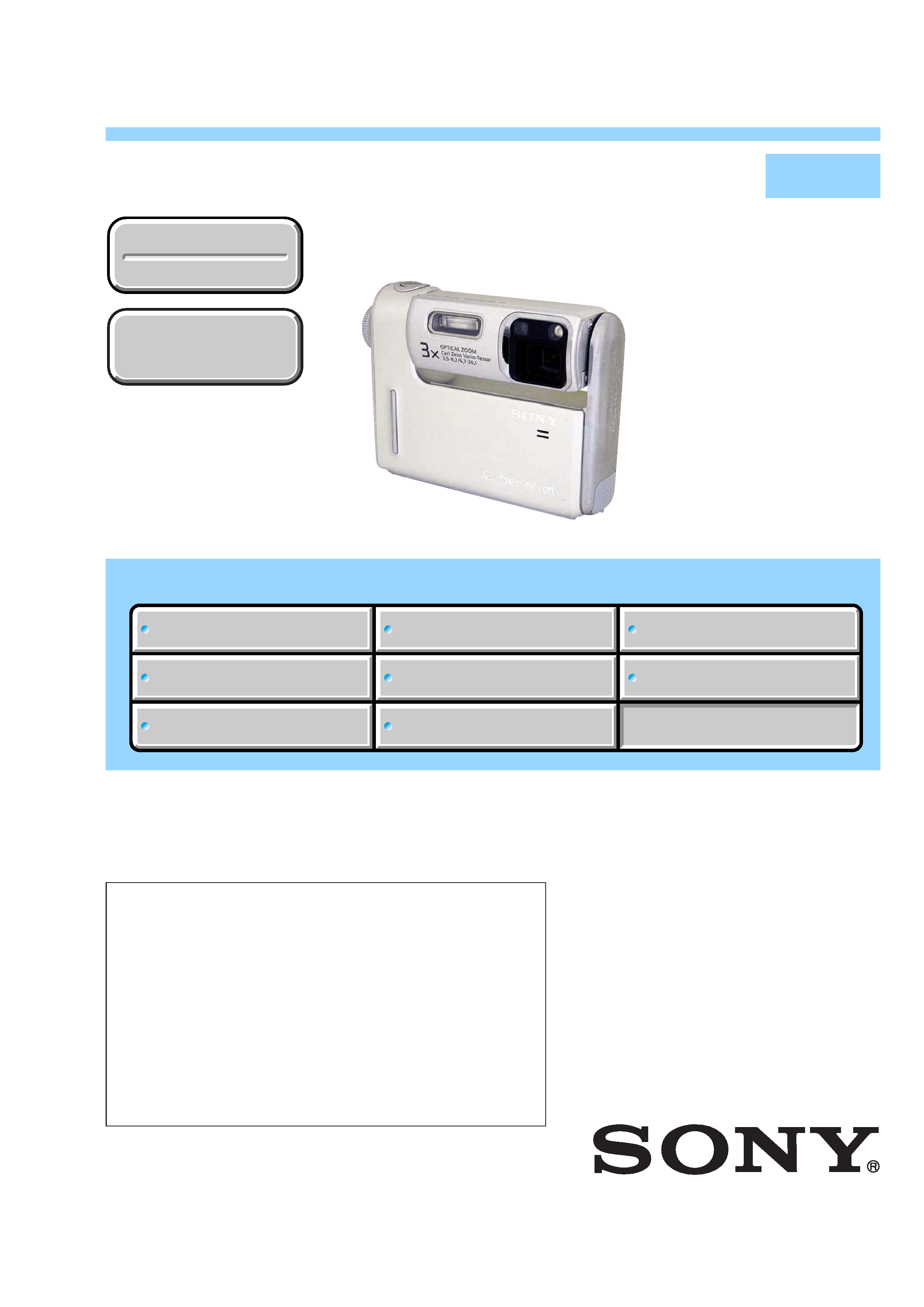
DIGITAL STILL CAMERA
On the CH-147 and SY-099 boards
This service manual procides the information that is premised the
circuit board replacement service and not intended repair inside the
CH-147 and SY-099 boards.
Therefore, schematic diagram, printed wiring board and electrical
parts list of the CH-147 and SY-099 boards are not shown.
The following pages are not shown.
Schematic diagram ................... Pages 4-9 to 4-28
Printed wiring board .................. Pages 4-43 to 4-46
Mounted parts location .............. Pages 4-54
Electrical parts list ..................... Pages 5-6 and 5-9 to 5-13
The above-described information is shown in service manual Level 3.
Photo: Silver
DSC-F88
2004E0500-1
©2004.5
Published by DI Technical Support Section
9-876-750-31
US Model
Canadian Model
AEP Model
UK Model
E Model
Hong Kong Model
Australian Model
Chinese Model
Korea Model
Tourist Model
Japanese Model

-- 2 --
DSC-F88
SPECIFICATIONS
[LCD screen]
LCD panel used
4.6 cm (1.8 type) TFT drive
Total number of dots
134 000 (560
×240) dots
[Input and Output connectors]
Multi connector
USB communication
Hi-Speed USB (USB 2.0 compliant)
[Power, general]
Used battery pack
NP-FR1
Power requirements
3.6 V
Power consumption (during shooting with LCD
screen on)
1.4 W
Operating temperature range
0
° to +40°C (32° to +104°F)
Storage temperature range
-20° to +60°C (-4° to +140°F)
Dimensions
97.8
× 74.4 × 25.6 mm
(3 7/8
× 3 × 1 1/16 inches)
(W/H/D, protruding portions not
included)
Mass
Approx. 163 g (5.7 oz) (battery pack
NP-FR1, "Memory Stick," wrist
strap, and so on included)
Microphone
Electret condenser microphone
Speaker
Dynamic speaker
Exif Print
Compatible
PRINT Image Matching II
Compatible
PictBridge
Compatible
x AC-LS5/LS5B AC Adaptor
Input rating
100 V to 240 V AC, 50/60 Hz, 11 W,
0.16 A to 0.09 A
Output rating 4.2 V DC, 1.5 A
Operating temperature range
0
° to +40°C (32° to +104°F)
Storage temperature range
-20° to +60°C (-4° to +140°F)
Dimensions (excluding projecting parts)
Approx. 48
× 29 × 81 mm
(1 15/16
× 1 3/16 × 3 1/4 inches)
(W/H/D)
Mass
Approx. 130 g (5 oz) excluding
power cord (mains lead)
x NP-FR1 battery pack
Used battery Lithium-ion battery
Maximum voltage
DC 4.2 V
Nominal voltage
DC 3.6 V
Capacity
4.4 Wh (1 220 mAh)
Accessories
· AC-LS5/LS5B AC Adaptor (1)
· Power cord (mains lead) (1)
· NP-FR1 battery pack (1)
· Battery case (1)
· USB multi cable (1)
· A/V multi cable (1)
· Wrist strap (1)
· "Memory Stick" (32MB) (1)
· CD-ROM (USB driver: SPVD-012) (1)
· Operating Instructions (1)
See page 5-14.
Design and specifications are subject to change
without notice.
x Camera
[System]
Image device 7.66 mm (1/2.4 type) color
CCD
Primary color filter
Total pixels number of camera
Approx. 5 255 000 pixels
Effective pixels number of camera
Approx. 5 090 000 pixels
Lens
Carl Zeiss Vario-Tessar
3
× zoom lens
f=6.7 to 20.1 mm (35 mm camera
conversion: 38 to 114 mm)
F3.5-4.2
Exposure control
Automatic, Manual exposure, Scene
selection (10 modes)
White balance
Automatic, Daylight, Cloudy,
Fluorescent, Incandescent
File format (DCF compliant)
Still images: Exif Ver. 2.2, JPEG
compliant, DPOF compatible
Movies: MPEG1 compliant
(Monaural)
Recording medium
"Memory Stick"
Flash
Recommended distance (when ISO
sensitivity is set to Auto)
0.15 to 2.2 m (6 inches to
7feet 2 5/8 inches) (W)
0.25 to 2 m (9 7/8 inches to
6feet 6 3/4 inches) (T)
-- 3 --
DSC-F88
SAFETY-RELATED COMPONENT WARNING!!
COMPONENTS IDENTIFIED BY MARK 0 OR DOTTED LINE WITH
MARK 0 ON THE SCHEMATIC DIAGRAMS AND IN THE PARTS
LIST ARE CRITICAL TO SAFE OPERATION. REPLACE THESE
COMPONENTS WITH SONY PARTS WHOSE PART NUMBERS
APPEAR AS SHOWN IN THIS MANUAL OR IN SUPPLEMENTS
PUBLISHED BY SONY.
ATTENTION AU COMPOSANT AYANT RAPPORT
À LA SÉCURITÉ!
LES COMPOSANTS IDENTIFÉS PAR UNE MARQUE 0 SUR LES
DIAGRAMMES SCHÉMATIQUES ET LA LISTE DES PIÈCES SONT
CRITIQUES POUR LA SÉCURITÉ DE FONCTIONNEMENT. NE
REMPLACER CES COMPOSANTS QUE PAR DES PIÈSES SONY
DONT LES NUMÉROS SONT DONNÉS DANS CE MANUEL OU
DANS LES SUPPÉMENTS PUBLIÉS PAR SONY.
1.
Check the area of your repair for unsoldered or poorly-soldered
connections. Check the entire board surface for solder splashes
and bridges.
2.
Check the interboard wiring to ensure that no wires are
"pinched" or contact high-wattage resistors.
3.
Look for unauthorized replacement parts, particularly
transistors, that were installed during a previous repair. Point
them out to the customer and recommend their replacement.
4.
Look for parts which, through functioning, show obvious signs
of deterioration. Point them out to the customer and
recommend their replacement.
5.
Check the B+ voltage to see it is at the values specified.
6.
Flexible Circuit Board Repairing
·Keep the temperature of the soldering iron around 270°C
during repairing.
· Do not touch the soldering iron on the same conductor of the
circuit board (within 3 times).
· Be careful not to apply force on the conductor when soldering
or unsoldering.
Unleaded solder
Boards requiring use of unleaded solder are printed with the lead-
free mark (LF) indicating the solder contains no lead.
(Caution: Some printed circuit boards may not come printed with
the lead free mark due to their particular size.)
: LEAD FREE MARK
Unleaded solder has the following characteristics.
· Unleaded solder melts at a temperature about 40
°C higher than
ordinary solder.
Ordinary soldering irons can be used but the iron tip has to be
applied to the solder joint for a slightly longer time.
Soldering irons using a temperature regulator should be set to
about 350
°C.
Caution: The printed pattern (copper foil) may peel away if the
heated tip is applied for too long, so be careful!
· Strong viscosity
Unleaded solder is more viscous (sticky, less prone to flow) than
ordinary solder so use caution not to let solder bridges occur such
as on IC pins, etc.
· Usable with ordinary solder
It is best to use only unleaded solder but unleaded solder may
also be added to ordinary solder.
SAFETY CHECK-OUT
After correcting the original service problem, perform the following
safety checks before releasing the set to the customer.
CAUTION
Danger of explosion if battery is incorrectly replaced.
Replace only with the same or equivalent type.

-- 4 --
DSC-F88
TABLE OF CONTENTS
1.
SERVICE NOTE
1-1.
Note for Repair ································································ 1-1
1-2.
Discharging of the DC-101 Flexible Board's Charging
Capacitor (C014) ····························································· 1-1
1-3.
Description on Self-diagnosis Display ···························· 1-2
2.
DISASSEMBLY
2-1.
Disassembly ····································································· 2-1
2-2.
Service Position ······························································· 2-5
2-3.
The Method of Attachment of FP-862 and FP-863
Flexible Boards ································································ 2-7
2-4.
Circuit Boards Location ·················································· 2-8
2-5.
Flexible Boards Location ················································ 2-8
3.
BLOCK DIAGRAMS
3-1.
Overall Block Diagram (1/2) ··········································· 3-1
3-2.
Overall Block Diagram (2/2) ··········································· 3-3
3-3.
Power Block Diagram (1/2) ············································· 3-5
3-4.
Power Block Diagram (2/2) ············································· 3-7
4.
PRINTED WIRING BOARDS AND
SCHEMATIC DIAGRAMS
4-1.
Frame Schematic Diagram ·············································· 4-1
4-2.
Schematic Diagrams ························································ 4-5
CD-495 FLEXIBLE (CCD IMAGER) ··························· 4-7
ST-094 FLEXIBLE (FLASH DRIVE) ························· 4-29
DC-101 FLEXIBLE (DC IN, FLASH CHARGE) ······· 4-31
JK-261 FLEXIBLE (MULTI CONNECTOR) ············· 4-33
KK-031 (LENS POSITION) ········································ 4-35
CONTROL SWITCH BLOCK (SW), (MODE) ··········· 4-35
FP-862 FLEXIBLE ······················································· 4-37
4-3.
Printed Wiring Boards ··················································· 4-39
CD-495 FLEXIBLE ······················································ 4-41
ST-094 FLEXIBLE ······················································· 4-47
DC-101 FLEXIBLE ······················································ 4-48
JK-261 FLEXIBLE ······················································· 4-49
KK-031 ·········································································· 4-50
4-4.
Mounted Parts Location ················································ 4-53
5.
REPAIR PARTS LIST
5-1.
Exploded Views ······························································· 5-2
5-1-1. Cabinet Block Section ····················································· 5-2
5-1-2. BT Holder Block Section ················································ 5-3
5-1-3. Lens Block Section ·························································· 5-4
5-2.
Electrical Parts List ························································· 5-5
Section
Title
Page
1-1
DSC-F88
1-2. DISCHARGING OF THE DC-101
FLEXIBLE BOARD'S CHARGING
CAPACITOR (C014)
The charging capacitor (C014) of the DC-101 flexible board is
charged up to the maximum 300 V potential.
There is a danger of electric shock by this high voltage when the
capacitor is handled by hand. The electric shock is caused by the
charged voltage which is kept without discharging when the main
power of the unit is simply turned off. Therefore, the remaining
voltage must be discharged as described below.
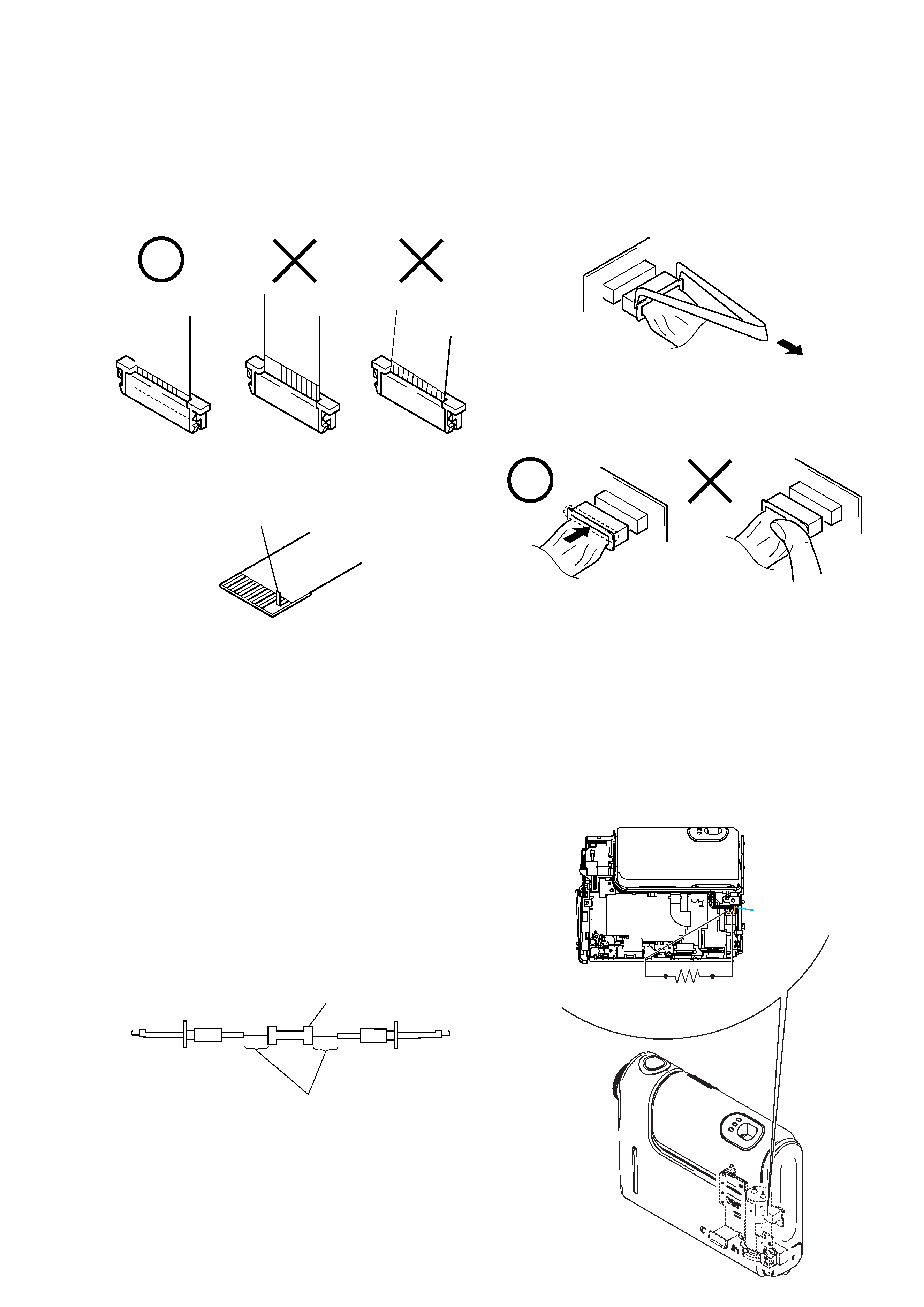
Preparing the Short Jig
To preparing the short jig, a small clip is attached to each end of a
resistor of 1 k
/1 W (1-215-869-11).
Wrap insulating tape fully around the leads of the resistor to prevent
electrical shock.
1 k
/1 W
Wrap insulating tape.
Discharging the Capacitor
Short-circuit between the positive and the negative terminals of
charged capacitor with the short jig about 10 seconds.
1-1. NOTE FOR REPAIR
Make sure that the flat cable and flexible board are not cracked of
bent at the terminal.
Do not insert the cable insufficiently nor crookedly.
Cut and remove the part of gilt
which comes off at the point.
(Be careful or some
pieces of gilt may be left inside)
When remove a connector, don't pull at wire of connector.
It is possible that a wire is snapped.
When installing a connector, don't press down at wire of connector.
It is possible that a wire is snapped.
SECTION 1
SERVICE NOTE
DC-101
(CN001)
R:1 k
/1 W
(Part code:
1-215-869-11)