SERVICE MANUAL
PORTABLE CD PLAYER
US Model
UK Model
D-NE330
E Model
D-NE330/NE331
SPECIFICATIONS
D-NE330/NE331
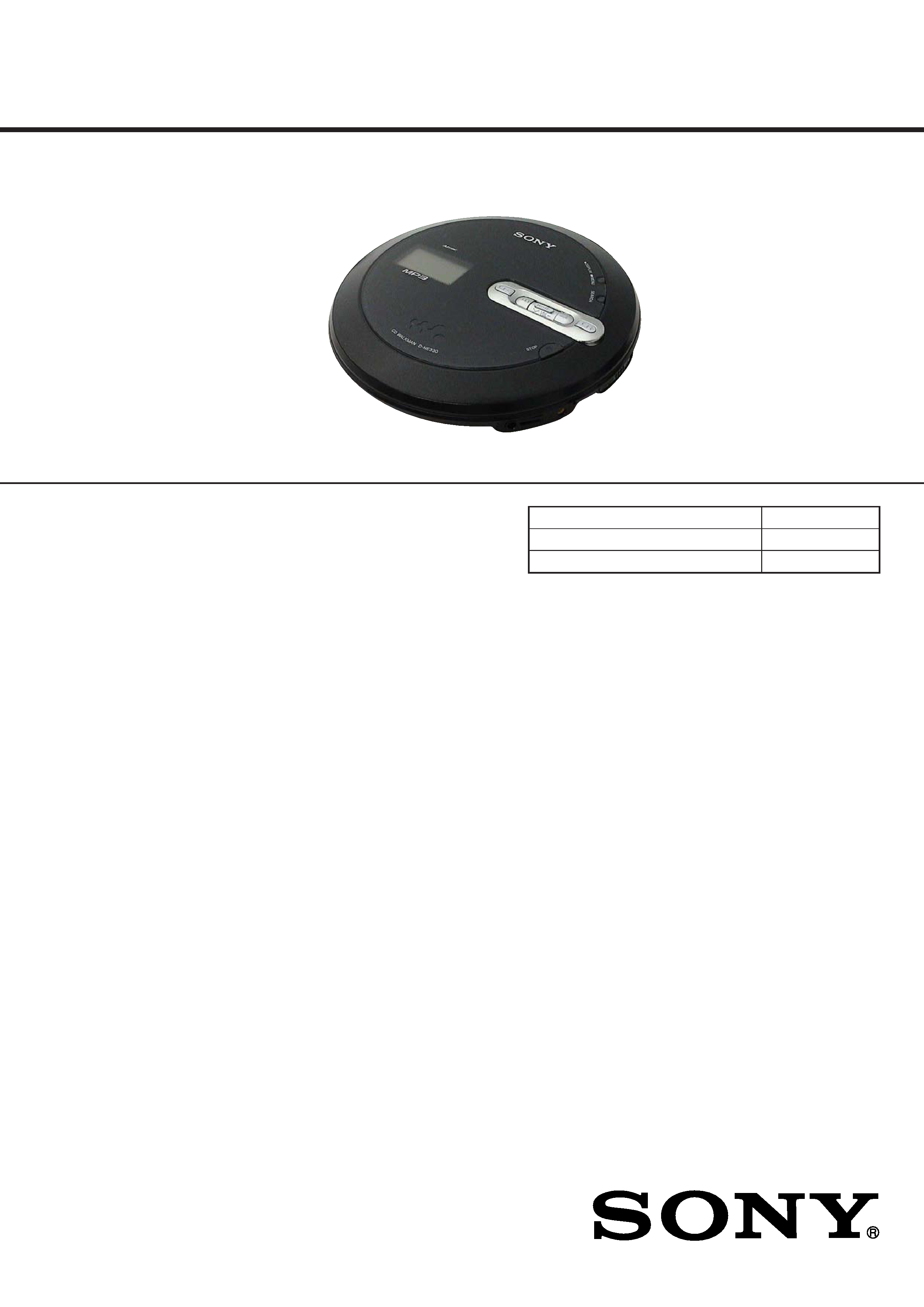
Photo: D-NE330
Ver. 1.0 2005.12
Model Name Using Similar Mechanism
D-NE320/NE321
CD Mechanism Type
CDM-3325ERV2
Optical Pick-up Name
DAX-25EV
9-879-984-01
2005L05-1
© 2005.12
Sony Corporation
Personal Audio Division
Published by Sony Engineering Corporation
Continued on next page
100 240 V 50/60
e area code of the model you
upper left side of the bar
AC power adaptor (Except NE330: US)
Earphones
REMOTE (NE330: US, UK/NE331)
Rechargeable battery (NE331)
Battery carring case (NE331)
Operating Instractions
Supplied Accessories
2
D-NE330/NE331
SAFETY-RELATED COMPONENT WARNING!!
COMPONENTS IDENTIFIED BY MARK 0 OR DOTTED LINE
WITH MARK 0 ON THE SCHEMATIC DIAGRAMS AND IN
THE PARTS LIST ARE CRITICAL TO SAFE OPERATION.
REPLACE THESE COMPONENTS WITH SONY PARTS WHOSE
PART NUMBERS APPEAR AS SHOWN IN THIS MANUAL OR
IN SUPPLEMENTS PUBLISHED BY SONY.
Notes on chip component replacement
· Never reuse a disconnected chip component.
· Notice that the minus side of a tantalum capacitor may be
damaged by heat.
Flexible Circuit Board Repairing
· Keep the temperature of the soldering iron around 270 °C
during repairing.
· Do not touch the soldering iron on the same conductor of the
circuit board (within 3 times).
· Be careful not to apply force on the conductor when soldering
or unsoldering.
CAUTION
Use of controls or adjustments or performance of procedures
other than those specified herein may result in hazardous radiation
exposure.

3
D-NE330/NE331
TABLE OF CONTENTS
1.
SERVICING NOTES ............................................... 4
2.
GENERAL ................................................................... 5
3.
DISASSEMBLY
3-1.
Disassembly Flow ...........................................................
6
3-2.
Cabinet Lower Sub Assy, Upper Lid Sub Assy ...............
6
3-3.
MAIN Board, Optical Pick-Up Assy
(CDM-3325ERV2) ..........................................................
7
3-4.
SWITCH Board ...............................................................
7
4.
DIAGRAMS
4-1.
Schematic Diagram MAIN Board (1/3) ....................
9
4-2.
Schematic Diagram MAIN Board (2/3) .................... 10
4-3.
Schematic Diagram MAIN Board (3/3) .................... 11
4-4.
Printed Wiring Board
MAIN Board (Component Side) .............................. 12
4-5.
Printed Wiring Board
MAIN Board (Conductor Side) ................................. 13
4-6.
Printed Wiring Board SWITCH Board ..................... 14
4-7.
Schematic Diagram SWITCH Board ........................ 15
5.
EXPLODED VIEWS
5-1.
Upper Lid Section ........................................................... 22
5-2.
Cabinet Lower Section .................................................... 23
5-3.
Optical Pick-Up Section (CDM-3325ERV2) .................. 24
6.
ELECTRICAL PARTS LIST ................................ 25
4
D-NE330/NE331
SECTION 1
SERVICING NOTES
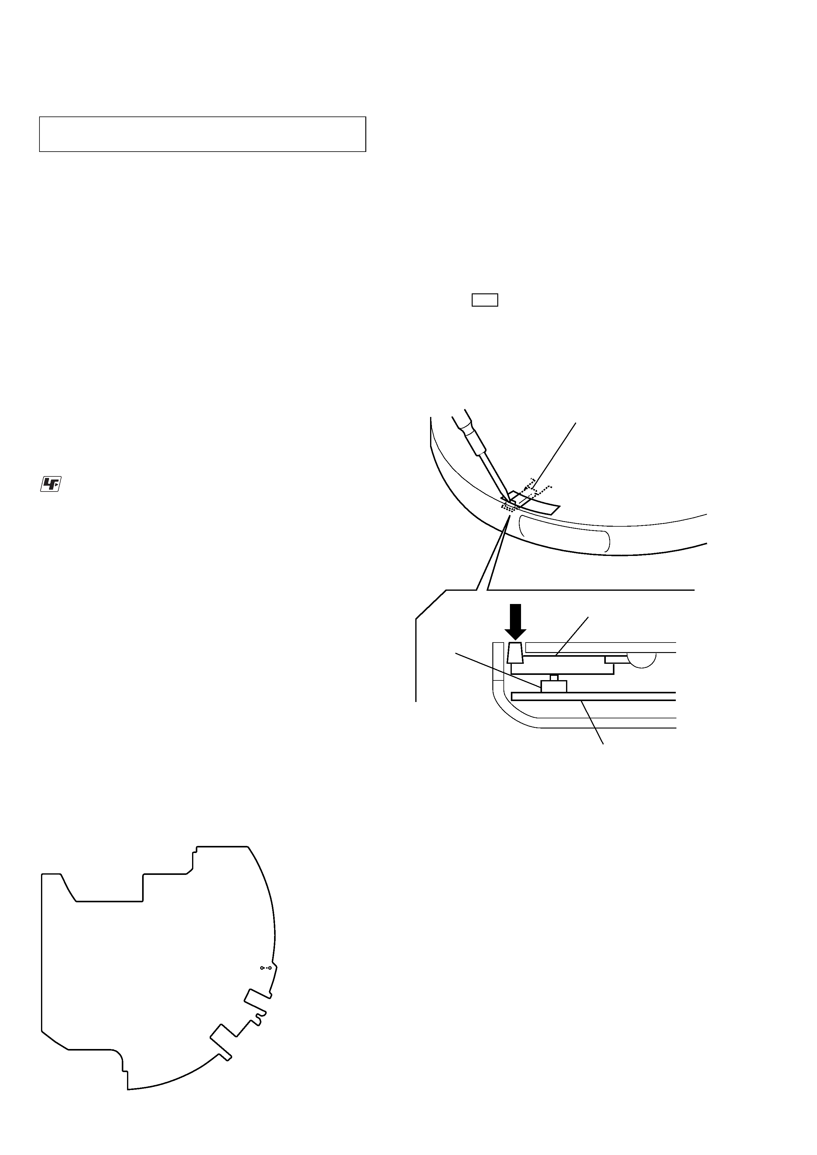
NOTES ON HANDLING THE OPTICAL PICK-UP
BLOCK OR BASE UNIT
The laser diode in the optical pick-up block may suffer electrostatic
break-down because of the potential difference generated by the
charged electrostatic load, etc. on clothing and the human body.
During repair, pay attention to electrostatic break-down and also
use the procedure in the printed matter which is included in the
repair parts.
The flexible board is easily damaged and should be handled with
care.
LASER DIODE AND FOCUS SEARCH OPERATION
CHECK
During normal operation of the equipment, emission of the laser
diode is prohibited unless the upper lid is closed while turning on
the S801. (push switch type)
The following checking method for the laser diode is operable.
· Method:
Emission of the laser diode is visually checked.
1. Open the upper lid.
2. With a disc not set, turn on the S801 with a screwdriver having
a thin tip as shown in Fig.1.
3. Press the u button.
4. Observing the objective lens, check that the laser diode emits
light.
When the laser diode does not emit light, automatic power
control circuit or optical pick-up is faulty.
In this operation, the objective lens will move up and down 2
times along with inward motion for the focus search.
NOTE ON REPLACEMENT OF MAIN BOARD OR
EEPROM (IC802)
When MAIN board is replaced or EEPROM (IC802) on the MAIN
board is replaced, patch processing is needed.
Confirm about information of patch processing to each service
headquarters.
NOTES ON LASER DIODE EMISSION CHECK
The laser beam on this model is concentrated so as to be focused on
the disc reflective surface by the objective lens in the optical pick-
up block. Therefore, when checking the laser diode emission,
observe from more than 30 cm away from the objective lens.
Fig. 1 Method to push the S801
UNLEADED SOLDER
Boards requiring use of unleaded solder are printed with the lead-
free mark (LF) indicating the solder contains no lead.
(Caution: Some printed circuit boards may not come printed with
the lead free mark due to their particular size)
: LEAD FREE MARK
Unleaded solder has the following characteristics.
· Unleaded solder melts at a temperature about 40 °C higher
than ordinary solder.
Ordinary soldering irons can be used but the iron tip has to be
applied to the solder joint for a slightly longer time.
Soldering irons using a temperature regulator should be set to
about 350
°C.
Caution: The printed pattern (copper foil) may peel away if
the heated tip is applied for too long, so be careful!
· Strong viscosity
Unleaded solder is more viscou-s (sticky, less prone to flow)
than ordinary solder so use caution not to let solder bridges
occur such as on IC pins, etc.
· Usable with ordinary solder
It is best to use only unleaded solder but unleaded solder may
also be added to ordinary solder.
OPERATION CHECK WHEN THE LID IS OPEN
In performing the repair with the power supplied to the set, removing
the MAIN board causes the set to be disabled.
In such a case, make a solder bridge to short SL805 (OPEN) on the
MAIN board in advance.
S801
lever (detector)
lever (detector)
MAIN board
SL805
(OPEN)
MAIN Board (Component Side)
5
D-NE330/NE331
SECTION 2
GENERAL
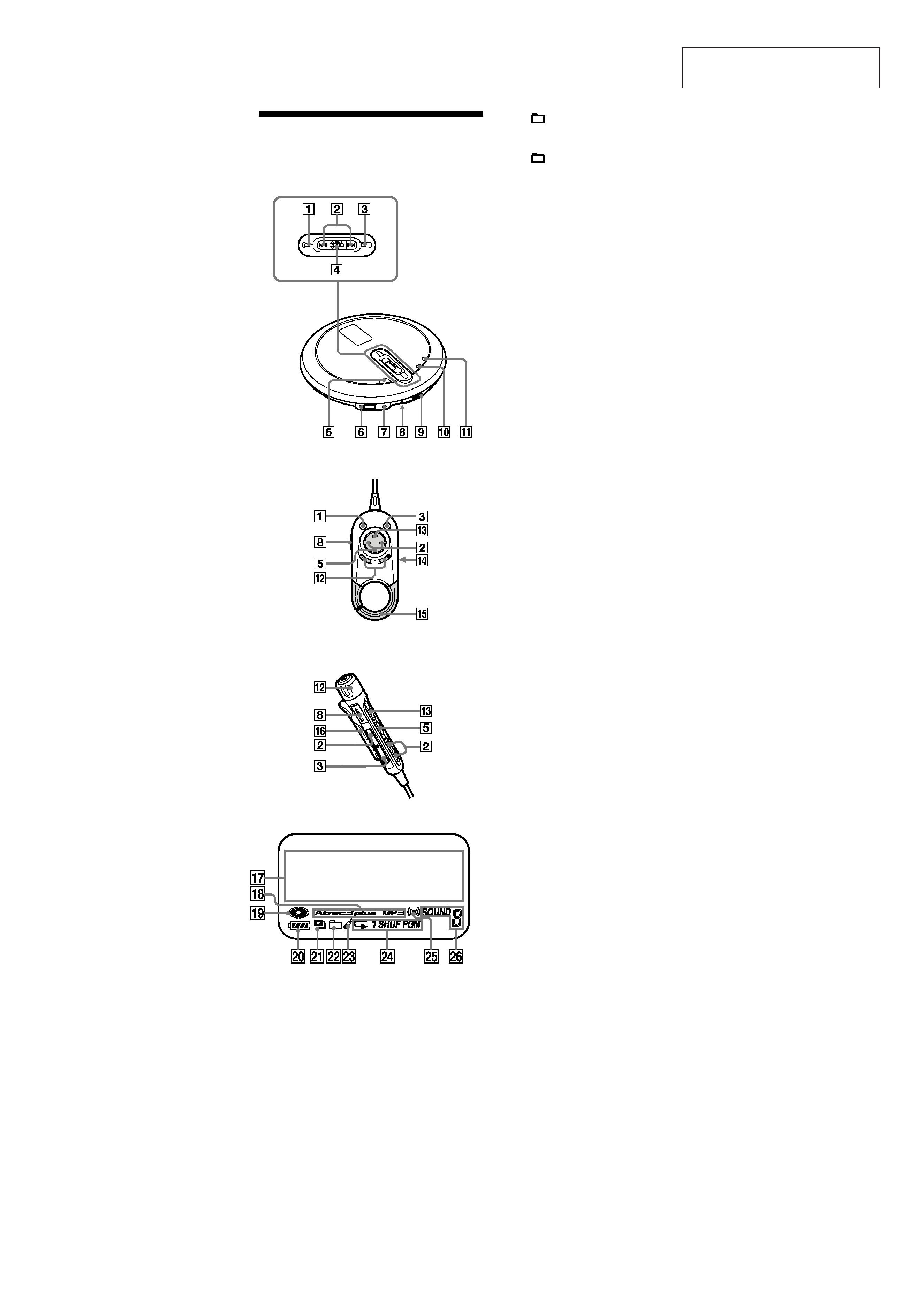
This section is extracted from
instruction manual.
NE330: US)
NE330: UK/NE331)
NE331)
NE330)
NE330: US)
NE330: UK/NE331)