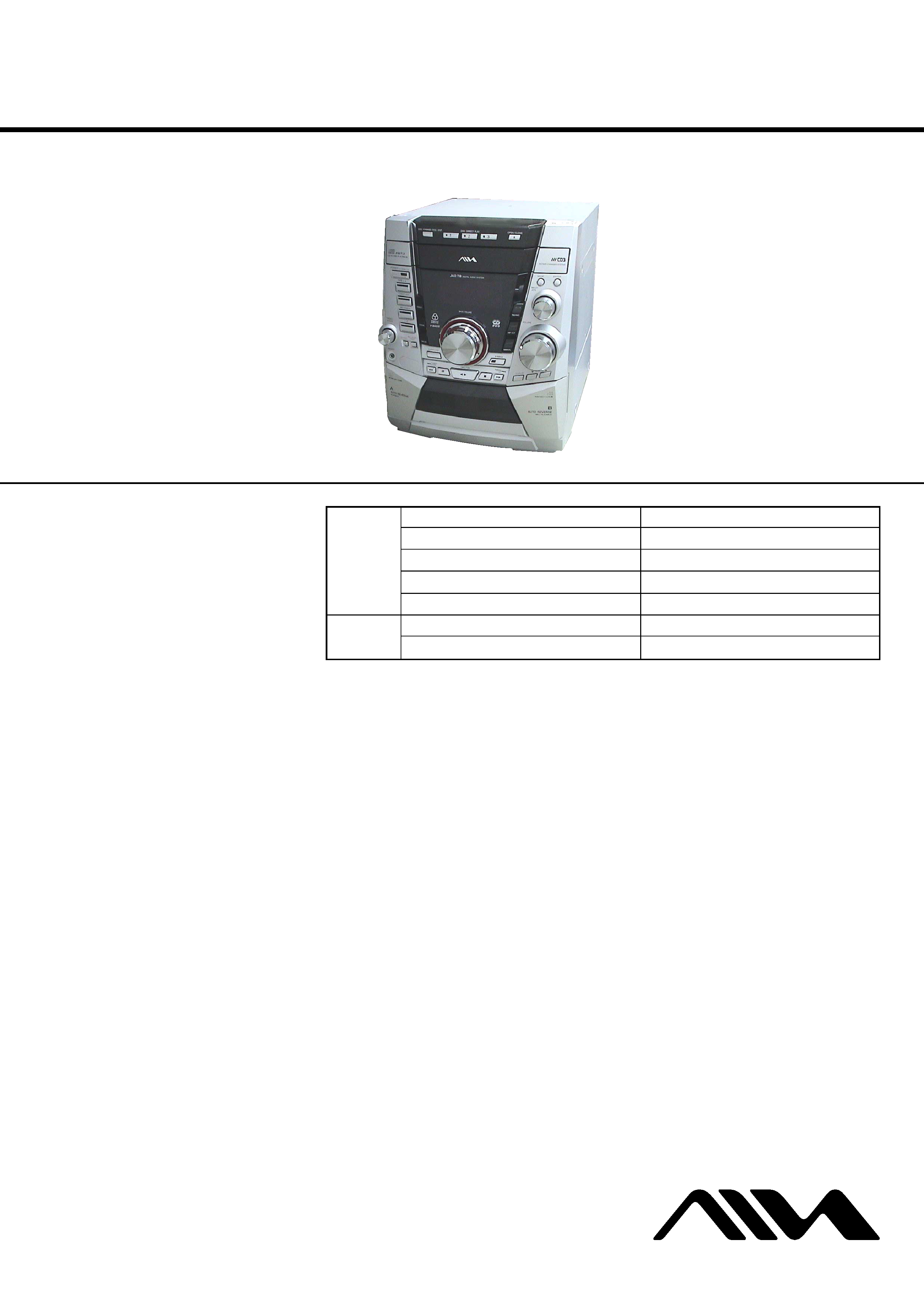
SERVICE MANUAL
COMPACT DISC DECK RECEIVER
E Model
CX-JT9
Ver 1.0 2003.05
9-877-262-01
Sony Corporation
2003E05-1
Home Audio Company
C
2003.05
Published by Sony Engineering Corporation
SPECIFICATIONS
CX-JT9 is the tuner, amplifier, cassette deck and
CD player section in JAX-PK9.
Model Name Using Similar Mechanism
NEW
CD
CD Mechanism Type
CDM74F-K6BD71A
Section
Base Unit Name
BU-K6BD71A
Optical Block Name
KSM-213DCP
Optical Pick-up Name
KSS-213D
Tape deck
Model Name Using Similar Mechanism
NEW
Section
Tape Transport Mechanism Type
CWM43RR23
TUNER
FM tuning range
87.5 MHz to 108 MHz
FM usable sensitivity (IHF)
13.2 dBf
FM antenna terminal
75 ohms (unbalanced)
AM tuning range
530 kHz to 1710 kHz (10 kHz step)
531 kHz to 1710 kHz (9 kHz step)
AM usable sensitivity
350 µV/m
AM antenna
Loop antenna
AMPLIFIER
Power output
Front:
Rated: 156 W + 156 W (6 ohms,
T.H.D. 1 %, 1 kHz)
Reference: 195 W + 195 W (6 ohms,
T.H.D. 10 %, 1 kHz)
Front and Surround:
320 W + 200 W (Front Speaker: 6
ohms, Surround Speaker: 8 ohms,
T.H.D. 10 %, 1 kHz/DIN AUDIO)
Total harmonic distortion
0.08 % (98 W, 1 kHz, 6 ohms, DIN
AUDIO)
Input
MD (VIDEO): 1.5 V
MIC: 1 mV (600 ohms)
Outputs
FRONT SPEAKER: 6 ohms or more
SURROUND SPEAKER: 8 ohms or
more
PHONES: 32 ohms or more
CASSETTE DECK
Track format
4 tracks, 2 channels stereo
Frequency response
50 Hz 8 kHz
Recording system
AC bias
Heads
Deck A: playback x 1
Deck B: recording/playback x 1,
erase x 1
CD PLAYER
Laser
Semiconductor laser
(
= 780 nm)
Emission duration:
continuous
D/A converter
1 bit dual
Signal-to-noise ratio
85 dB (1 kHz, 0 dB)
Harmonic distortion
0.05 % (1 kHz, 0 dB)
GENERAL
Power requirements
120 V/220 V/230 V-240 V AC
(Switchable), 50 Hz/60 Hz
Power consumption
255 W
Power consumption
With ECO mode on: 0.25 W
in standby mode
With ECO mode off: 28 W
Dimensions (W x H x D)
280 x 328 x 446 mm
Weight
11.2 kg
Specifications and external appearance are subject to change
without notice.
COPYRIGHT
Check copyright laws relevant to recordings from discs, tuner
or tape for the country where the unit is to be used.
Licensed by BBE Sound, Inc. under USP4638258, 5510752
and 5736897.
CX-JT9
2
Notes on chip component replacement
·Never reuse a disconnected chip component.
· Notice that the minus side of a tantalum capacitor may be dam-
aged by heat.
Flexible Circuit Board Repairing
·Keep the temperature of the soldering iron around 270 °C dur-
ing repairing.
· Do not touch the soldering iron on the same conductor of the
circuit board (within 3 times).
· Be careful not to apply force on the conductor when soldering
or unsoldering.
CAUTION
Use of controls or adjustments or performance of procedures
other than those specified herein may result in hazardous ra-
diation exposure.
SAFETY-RELATED COMPONENT WARNING!!
COMPONENTS IDENTIFIED BY MARK 0 OR DOTTED
LINE WITH MARK 0 ON THE SCHEMATIC DIAGRAMS
AND IN THE PARTS LIST ARE CRITICAL TO SAFE
OPERATION. REPLACE THESE COMPONENTS WITH
SONY PARTS WHOSE PART NUMBERS APPEAR AS
SHOWN IN THIS MANUAL OR IN SUPPLEMENTS PUB-
LISHED BY SONY.
CLASS 1 LASER PRODUCT
LUOKAN 1 LASER LAITE
KLASS 1 LASER APPARAT
This appliance is classified
as a CLASS 1 LASER
product.
This label is located on the
rear exterior.

CX-JT9
3
TABLE OF CONTENTS
1.
SERVICING NOTES ................................................ 4
2.
GENERAL
Location of Controls .......................................................
7
3.
DISASSEMBLY
3-1. Disassembly Flow ...........................................................
9
3-2. Case (SIDE-L/R) ............................................................. 10
3-3. Case (Top) ....................................................................... 10
3-4. Tray Panel ........................................................................ 11
3-5. CD Mechanism Deck (CDM74F-K6BD71A) ................ 11
3-6. Front Panel Section ......................................................... 12
3-7. Mechanical Deck ............................................................. 12
3-8. Rear Cabinet Section ...................................................... 13
3-9. Main Board ...................................................................... 13
3-10. Power Board .................................................................... 14
3-11. Transformer Board .......................................................... 14
3-12 Table Assy ....................................................................... 15
3-13. Motor (TB) Board ........................................................... 15
3-14. Motor (LD) Board ........................................................... 16
3-15. Base Unit (BU-K6BD71A) ............................................. 16
3-16. Motor Gear Assy (Sled) (M701), BD Board .................. 17
3-17. Optical Pick-up (KSS-213D) .......................................... 17
4.
TEST MODE .............................................................. 18
5.
ELECTRICAL ADJUSTMENTS
CD Section ...................................................................... 21
6.
DIAGRAMS
6-1. Block Diagram CD Section ..................................... 22
6-2. Block Diagram TUNER/TAPE/PANEL Section ..... 23
6-3. Block Diagram AMP/POWER SUPPLY Section ... 24
6-4. Note for Printed Wiring Boards and
Schematic Diagrams ....................................................... 25
6-5. Printed Wiring Board BD Board ............................. 26
6-6. Schematic Diagram BD Board ................................ 27
6-7. Printed Wiring Boards CHANGER Section ............ 28
6-8. Schematic Diagram CHANGER Section ................ 29
6-9. Schematic Diagram
MAIN Board (1/4) (Suffix-11) ................................. 30
6-10. Schematic Diagram
MAIN Board (2/4) (Suffix-11) ................................. 31
6-11. Schematic Diagram
MAIN Board (3/4) (Suffix-11) ................................. 32
6-12. Schematic Diagram
MAIN Board (4/4) (Suffix-11) ................................. 33
6-13. Printed Wiring Board MAIN Board (Suffix-11) ..... 34
6-14. Printed Wiring Board MAIN Board (Suffix-13) ..... 35
6-15. Schematic Diagram
MAIN Board (1/4) (Suffix-13) ................................. 36
6-16. Schematic Diagram
MAIN Board (2/4) (Suffix-13) ................................. 37
6-17. Schematic Diagram
MAIN Board (3/4) (Suffix-13) ................................. 38
6-18. Schematic Diagram
MAIN Board (4/4) (Suffix-13) ................................. 39
6-19. Printed Wiring Board Power Board (E51 model) ... 40
6-20. Printed Wiring Board Power Board (MX model) ... 41
6-21. Schematic Diagram Power Board (1/2) ................... 42
6-22. Schematic Diagram Power Board (2/2) ................... 43
6-23. Printed Wiring Boards CD BUTTON/
HEADPHONE/MICROPHONE Boards ..................... 44
6-24. Schematic Diagram CD BUTTON/
HEADPHONE/MICROPHONE Boards ..................... 45
6-25. Printed Wiring Board PANEL Board ...................... 46
6-26. Schematic Diagram PANEL Board ......................... 47
6-27. Printed Wiring Board TRANSFORMER Board
(E51 model) ..................................................................... 48
6-28. Printed Wiring Board TRANSFORMER Board
(MX model) ..................................................................... 49
6-29. Schematic Diagram TRANSFORMER Board
(E51 model) ..................................................................... 50
6-30. Schematic Diagram TRANSFORMER Board
(MX model) ..................................................................... 51
6-31. IC Pin Function Description ........................................... 55
7.
EXPLODED VIEWS
7-1. Case Section .................................................................... 61
7-2. Front Panel Section-1 ...................................................... 62
7-3. Front Panel Section-2 ...................................................... 63
7-4. Front Panel Section-3 ...................................................... 64
7-5. Front Panel Section-4 ...................................................... 65
7-6. Chassis Section-1 ............................................................ 66
7-7. Chassis Section-2 ............................................................ 67
7-8. CD Mechanism Deck Section-1
(CDM74F-K6BD71A) .................................................... 68
7-9. CD Mechanism Deck Section-2
(CDM74F-K6BD71A) .................................................... 69
7-10. CD Mechanism Deck Section-3
(CDM74F-K6BD71A) .................................................... 70
7-11. Base Unit Section (BU-K6BD71A) ............................... 71
8.
ELECTRICAL PARTS LIST ............................... 72
·Abbreviation
E51 : Chilean and Peruvian models
MX
: Mexican model
4
CX-JT9
SECTION 1
SERVICING NOTES
NOTES ON HANDLING THE OPTICAL PICK-UP
BLOCK OR BASE UNIT
The laser diode in the optical pick-up block may suffer electro-
static break-down because of the potential difference generated
by the charged electrostatic load, etc. on clothing and the human
body.
During repair, pay attention to electrostatic break-down and also
use the procedure in the printed matter which is included in the
repair parts.
The flexible board is easily damaged and should be handled with
care.
NOTES ON LASER DIODE EMISSION CHECK
The laser beam on this model is concentrated so as to be focused
on the disc reflective surface by the objective lens in the optical
pick-up block. Therefore, when checking the laser diode emis-
sion, observe from more than 30 cm away from the objective lens.
LASER DIODE AND FOCUS SEARCH OPERATION
CHECK
Carry out the "S curve check" in "CD section adjustment" and
check that the S curve waveforms is output three times.
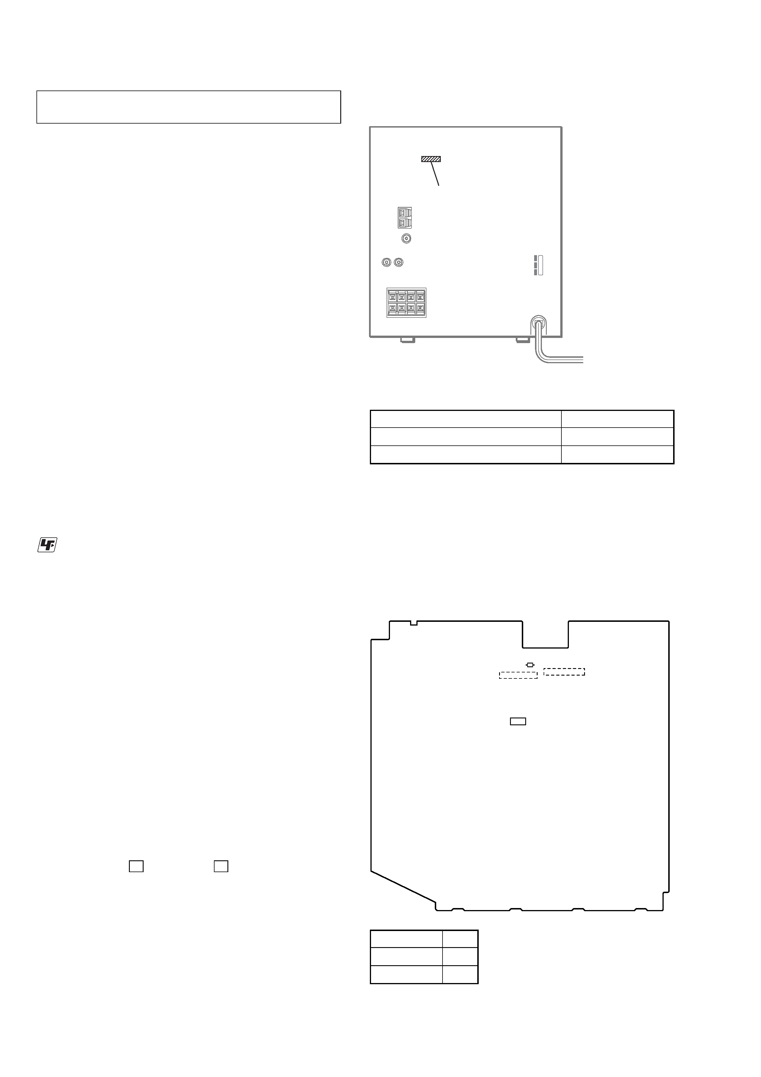
· MODEL IDENTIFICATION
Back Panel
MODEL
PART No.
Chilean and Peruvian models
4-245-109-0[]
Mexican model
4-245-109-2[]
PART No.
UNLEADED SOLDER
Boards requiring use of unleaded solder are printed with the lead-
free mark (LF) indicating the solder contains no lead.
(Caution: Some printed circuit boards may not come printed with
the lead free mark due to their particular size)
: LEAD FREE MARK
Unleaded solder has the following characteristics.
· Unleaded solder melts at a temperature about 40 °C higher than
ordinary solder.
Ordinary soldering irons can be used but the iron tip has to be
applied to the solder joint for a slightly longer time.
Soldering irons using a temperature regulator should be set to
about 350 °C.
Caution: The printed pattern (copper foil) may peel away if the
heated tip is applied for too long, so be careful!
· Strong viscosity
Unleaded solder is more viscou-s (sticky, less prone to flow)
than ordinary solder so use caution not to let solder bridges oc-
cur such as on IC pins, etc.
· Usable with ordinary solder
It is best to use only unleaded solder but unleaded solder may
also be added to ordinary solder.
D324
CN309
IC303
CN312
MAIN BOARD (Conductor Side)
· DISCRIMINATION
Either type of the MAIN board, Part No. 1-688-080-11 or 1-688-
080-13 is used for Chilean and Peruvian models.
Note: For Mexican model, only one type of the MAIN board, Part No. 1-
688-080-13 is used.
How to identify the type is described below.
D324
Suffix-11
×
Suffix-13
a
RELEASING THE DISC TRAY LOCK
The disc tray lock function for the antitheft of an demonstration
disc in the store is equipped.
Releasing Procedure :
While pressing the x key, press the Z key for 5 seconds. The
message "UNLOCKED" is displayed and the tray is unlocked.
Note: When "LOCKED" is displayed, the tray lock is not released by
turning power on/off with the [POWER] key.
5
CX-JT9
HOW TO OPEN THE DISC TRAY WHEN POWER SWITCH TURNS OFF.
2
Turn the loading gear
in the direction of arrow A.
1
Remove the case (side-L).
A
3
Pull-out the disc tray.