1
Ver 1.0 2001. 01
Model Name Using Similar Mechanism
NEW
CD Drive Mechanism Type
MG-393X-121//K
Optical Pick-up Name
KSS-720A
SERVICE MANUAL
US Model
Canadian Model
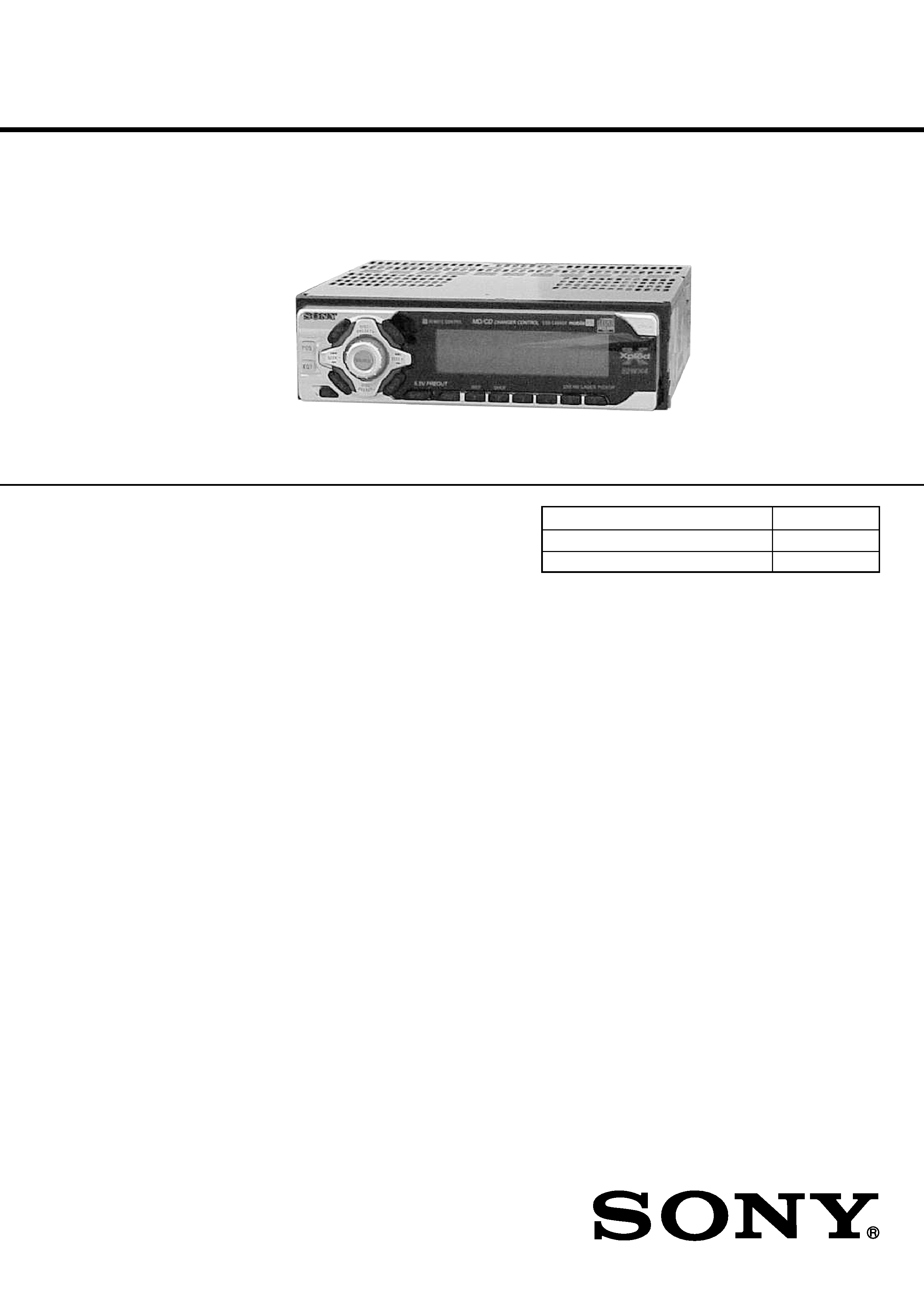
CDX-CA650X/CA660X
E Model
CDX-CA690X
CDX-CA650X/CA660X/CA690X
FM/AM COMPACT DISC PLAYER
AUDIO POWER SPECIFICATIONS (US Model)
POWER OUTPUT AND TOTAL HARMONIC DISTORTION
23 watts per channel minimum continuous average power into
4 ohms, 4 channels driven from 20 Hz to 20 kHz with no more
than 5% total harmonic distortion.
CD player section
Signal-to-noise ratio
90 dB
Frequency response
10 20,000 Hz
Wow and flutter
Below measurable limit
Laser Diode Properties (US, Canadian Model)
Material
GaAlAs
Wavelength
780 nm
Emission Duration
Continuous
Laser output power
Less than 44.6 µW*
* This output is the value measured at a distance
of 200 mm from the objective lens surface on the
Optical Pick-up Block.
Tuner section
FM
Tuning range
87.5 107.9 MHz (US, Canadian model)
FM tuning interval (E Model):
50 kHz/200 kHz switchable
87.5 108 MHz (at 50 kHz step)
87.5 107.9 MHz (at 200 kHz step)
Antenna terminal
External Antenna connector
Intermediate frequency 10.7 MHz/450 kHz
Usable sensitivity
8 dBf
Selectivity
75 dB at 400 kHz
Signal-to-noise ratio
66 dB (stereo),
72 dB (mono)
Harmonic distortion at 1 kHz
0.6% (stereo),
0.3% (mono)
Separation
35 dB at 1 kHz
Frequency response
30 15,000 Hz
AM
Tuning range
530 1,710 kHz (US, Canadian model)
AM tuning interval (E model):
9 kHz/10 kHz switchable
531 1,602 kHz (at 9 kHz step)
530 1,710 kHz (at 10 kHz step)
Antenna terminal
External Antenna connector
Intermediate frequency 10.7 MHz/450 kHz
Sensitivity
30 µV
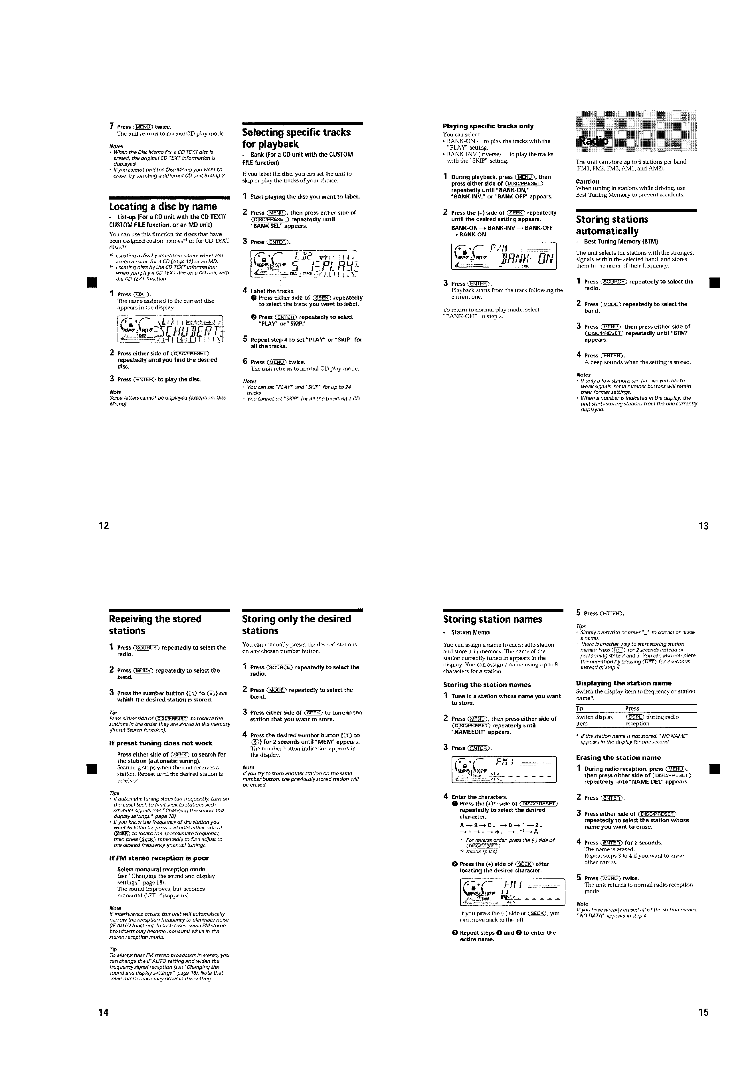
SPECIFICATIONS
Power amplifier section
Outputs
Speaker outputs
(sure seal connectors)
Speaker impedance
4 8 ohms
Maximum power output 50 W
× 4 (at 4 ohms)
General
Outputs
Audio outputs
Power Antenna relay control lead
Power amplifier control lead
Inputs
Telephone ATT control lead
Tone controls
Bass ±10 dB at 62 Hz (US, Canadian model)
Bass ±8 dB at 100 Hz (E model)
Treble ±10 dB at 16 kHz (US, Canadian model)
Treble ±8 dB at 10 kHz (E model)
Loudness (E model)
+8 dB at 100 Hz
+2 dB at 10 kHz
Power requirements
12 V DC car battery
(negative ground)
Dimensions
Approx. 178
× 50 × 176 mm
(7 1/8
× 2 × 7 in.) (w/h/d)
Mounting dimensions
Approx. 182
× 53 × 161 mm
(7 1/4
× 2 1/8 × 6 3/8 in.) (w/h/d)
Mass
Approx. 1.2 kg
(2 lb. 10 oz.)
Supplied accessories
Parts for installation and connections (1 set)
Front panel case (1)
Card remote commander
RM-X114
Note
This unit cannot be connected to a digital preamplifier or an equalizer.
Design and specifications are subject to change without
notice.
Photo: CDX-CA660X
· The tuner and CD sections have no adjustments.
Sony Corporation
Audio Entertainment Group
General Engineering Dept.
9-870-259-11
2001A0400-1
© 2001. 1
2
CDX-CA650X/CA660X/CA690X
SERVICE NOTES
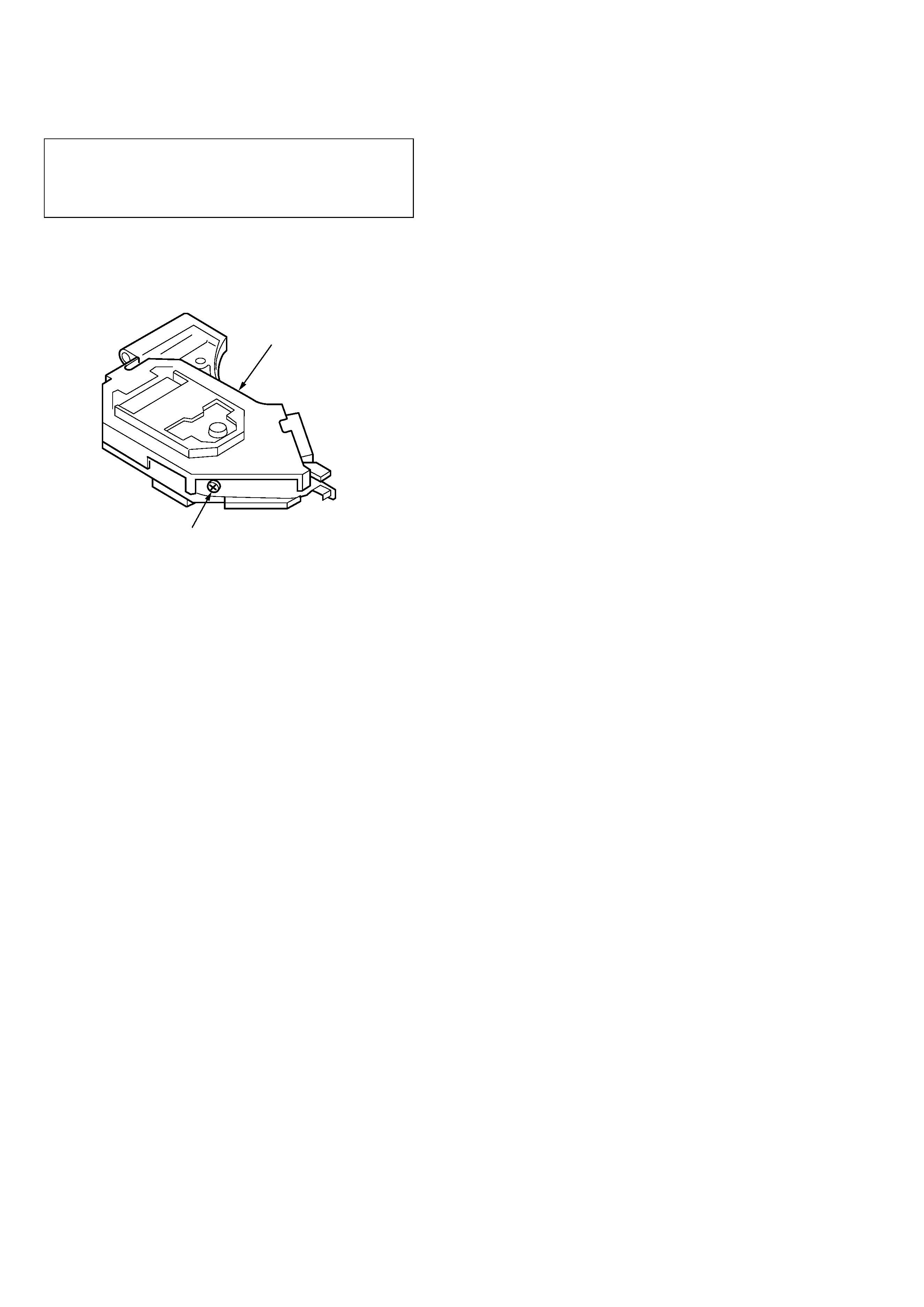
If the optical pick-up block is defective, please replace the whole
optical pick-up block.
Never turn the semi-fixed resistor located at the side of optical
pick-up block.
CAUTION
Use of controls or adjustments or performance of procedures
other than those specified herein may result in hazardous
radiation exposure.
NOTES ON HANDLING THE OPTICAL PICK-UP BLOCK
OR BASE UNIT
The laser diode in the optical pick-up block may suffer electrostatic
breakdown because of the potential difference generated by the
charged electrostatic load, etc. on clothing and the human body.
During repair, pay attention to electrostatic breakdown and also use
the procedure in the printed matter which is included in the repair
parts.
The flexible board is easily damaged and should be handled with
care.
NOTES ON LASER DIODE EMISSION CHECK
The laser beam on this model is concentrated so as to be focused on
the disc reflective surface by the objective lens in the optical pick-
up block. Therefore, when checking the laser diode emission, ob-
serve from more than 30 cm away from the objective lens.
Notes on Chip Component Replacement
· Never reuse a disconnected chip component.
· Notice that the minus side of a tantalum capacitor may be dam-
aged by heat.
TABLE OF CONTENTS
1. GENERAL
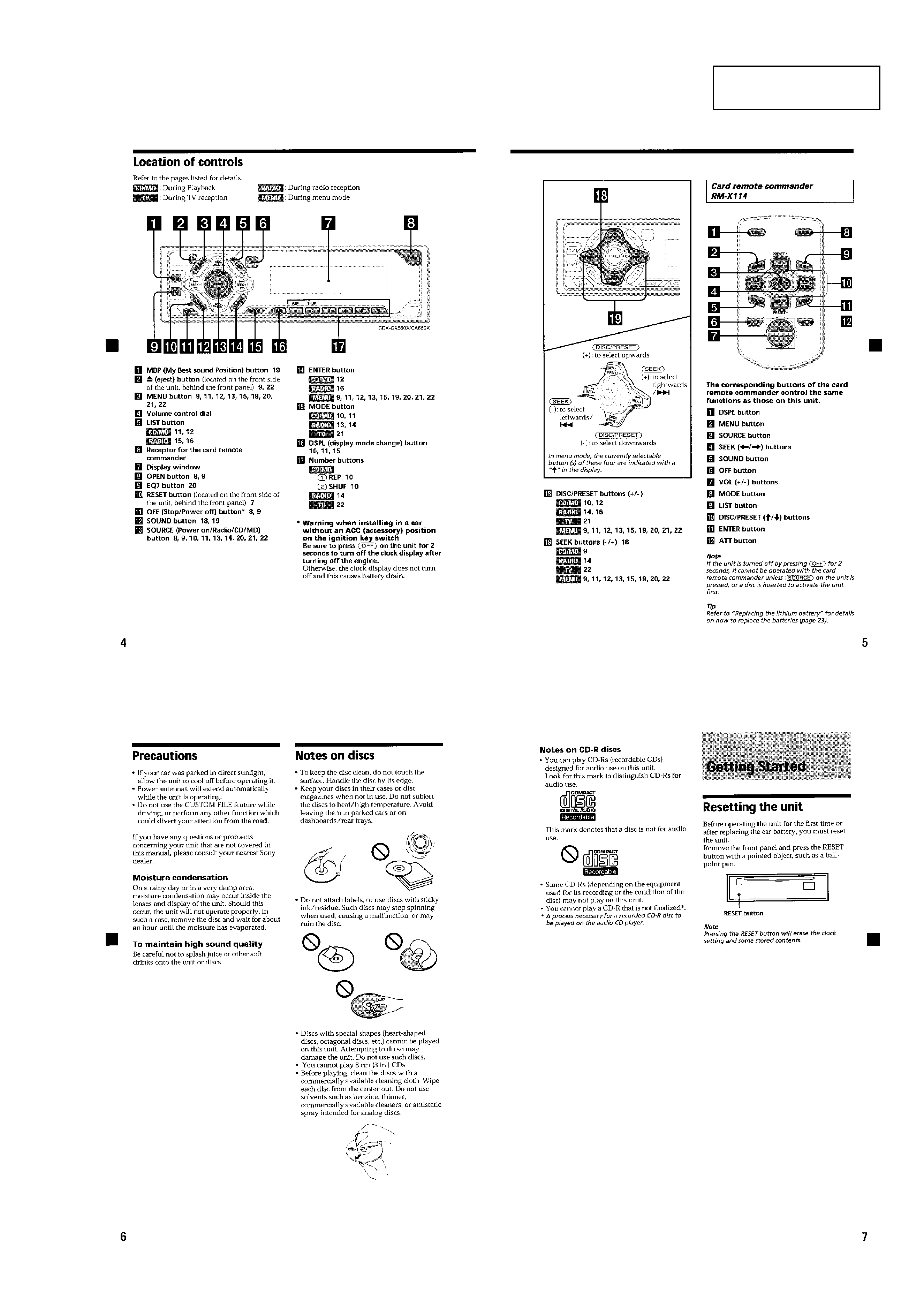
Location of controls ................................................................. 3
Getting Started ......................................................................... 3
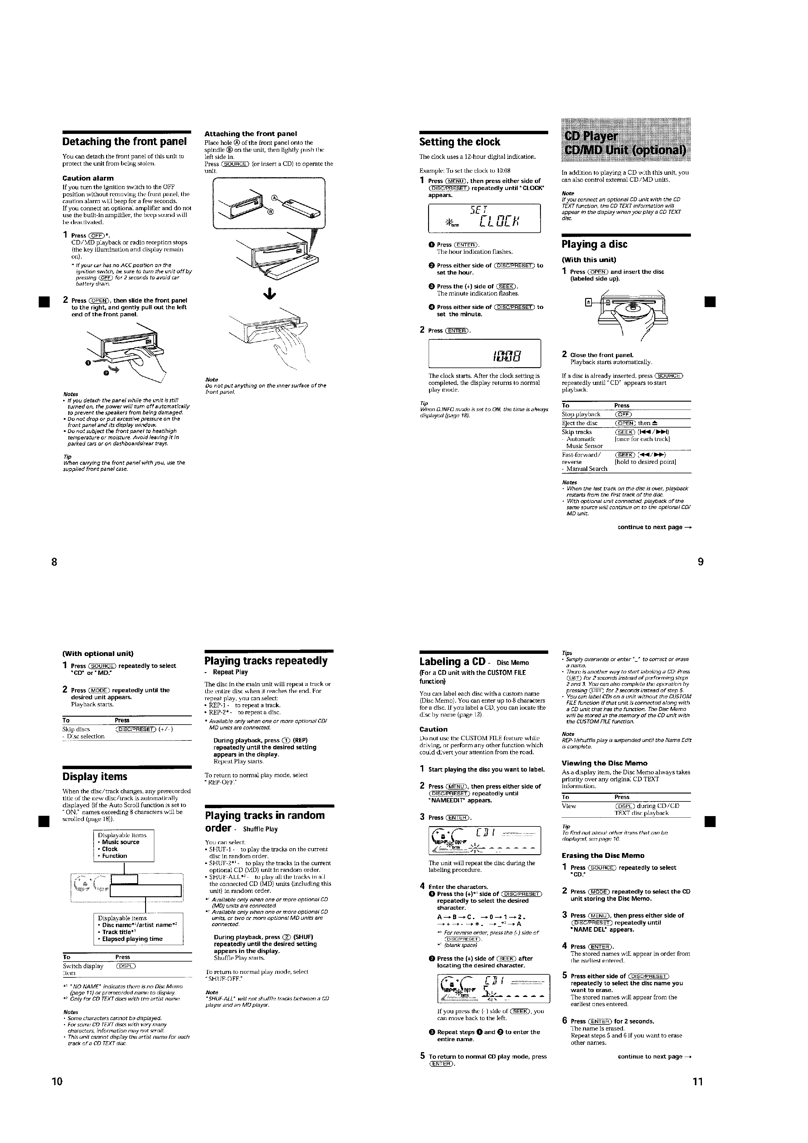
CD Player ................................................................................ 4
Radio ....................................................................................... 5
Other Functions ....................................................................... 6
Connection Diagram ................................................................ 7
2. DISASSEMBLY
2-1. Sub Panel (CD) Assy ........................................................... 8
2-2. CD Mechanism Block ......................................................... 8
2-3. Main Board ......................................................................... 8
2-4. Heat Sink (Main) ................................................................. 9
2-5. Chassis (T) Sub Assy .......................................................... 9
2-6. Lever Section .................................................................... 10
2-7. Servo Board ....................................................................... 10
2-8. Arm Roller Assy ................................................................ 11
2-9. Floating Block ................................................................... 11
2-10. Optical Pick-up Block ....................................................... 12
3. DIAGRAMS
3-1. IC Pin Descriptions ........................................................... 13
3-2. Block Diagram CD Section ........................................... 15
3-3. Block Diagram Tuner Section ....................................... 16
3-4. Block Diagram Display Section .................................... 17
3-5. Circuit Boards Location .................................................... 17
3-6. Printed Wiring Boards CD Mechanism Section ............ 18
3-7. Schematic Diagram CD Mechanism Section ................ 20
3-8. Printed Wiring Boards Main Section ............................ 21
3-9. Schematic Diagram Main Section (1/2) ........................ 22
3-10. Schematic Diagram Main Section (2/2) ........................ 23
3-11. Printed Wiring Board Relay Section ............................. 24
3-12. Schematic Diagram Relay Section ................................ 25
3-13. Schematic Diagram Display Section ............................. 26
3-14. Printed Wiring Board Display Section .......................... 27
4. EXPLODED VIEWS
4-1. Chassis Section ................................................................. 30
4-2. Front panel Section ........................................................... 31
4-3. CD Mechanism Section (1) ............................................... 32
4-4. CD Mechanism Section (2) ............................................... 33
4-5. CD Mechanism Section (3) ............................................... 34
5. ELECTRICAL PARTS LIST ........................................ 35
optical pick-up block
semi-fixed resistor
SAFETY-RELATED COMPONENT WARNING!!
COMPONENTS IDENTIFIED BY MARK 0 OR DOTTED LINE
WITH MARK 0 ON THE SCHEMATIC DIAGRAMS AND IN
THE PARTS LIST ARE CRITICAL TO SAFE OPERATION.
REPLACE THESE COMPONENTS WITH SONY PARTS WHOSE
PART NUMBERS APPEAR AS SHOWN IN THIS MANUAL OR
IN SUPPLEMENTS PUBLISHED BY SONY.
ATTENTION AU COMPOSANT AYANT RAPPORT
À LA SÉCURITÉ!!
LES COMPOSANTS IDENTIFIÉS PAR UNE MARQUE 0 SUR LES
DIAGRAMMES SCHÉMATIQUES ET LA LISTE DES PIÈCES
SONT CRITIQUES POUR LA SÉCURITÉ DE FONCTIONNEMENT.
NE REMPLACER CES COMPOSANTS QUE PAR DES PIÈCES
SONY DONT LES NUMÉROS SONT DONNÉS DANS CE MANUEL
OU DANS LES SUPPLÉMENTS PUBLIÉS PAR SONY.
3
CDX-CA650X/CA660X/CA690X
SECTION 1
GENERAL
This section is extracted
from instruction manual.
4
CDX-CA650X/CA660X/CA690X
5
CDX-CA650X/CA660X/CA690X