SERVICE MANUAL
US Model
Canadian Model
CDX-C7850
When performing service and inspection, check the suffix of the part number of
the main and relay boards.
(ECN-CSA00017)
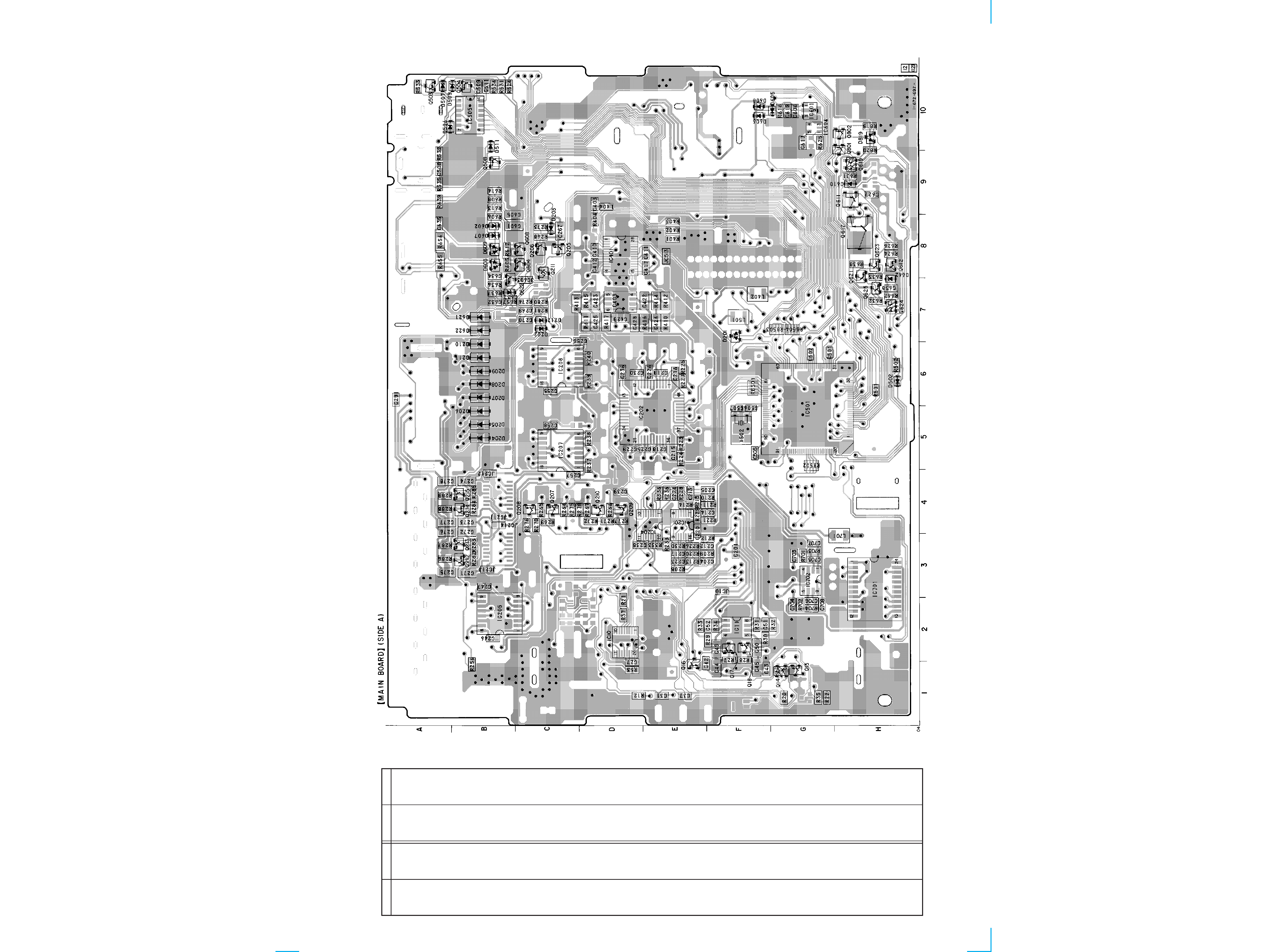
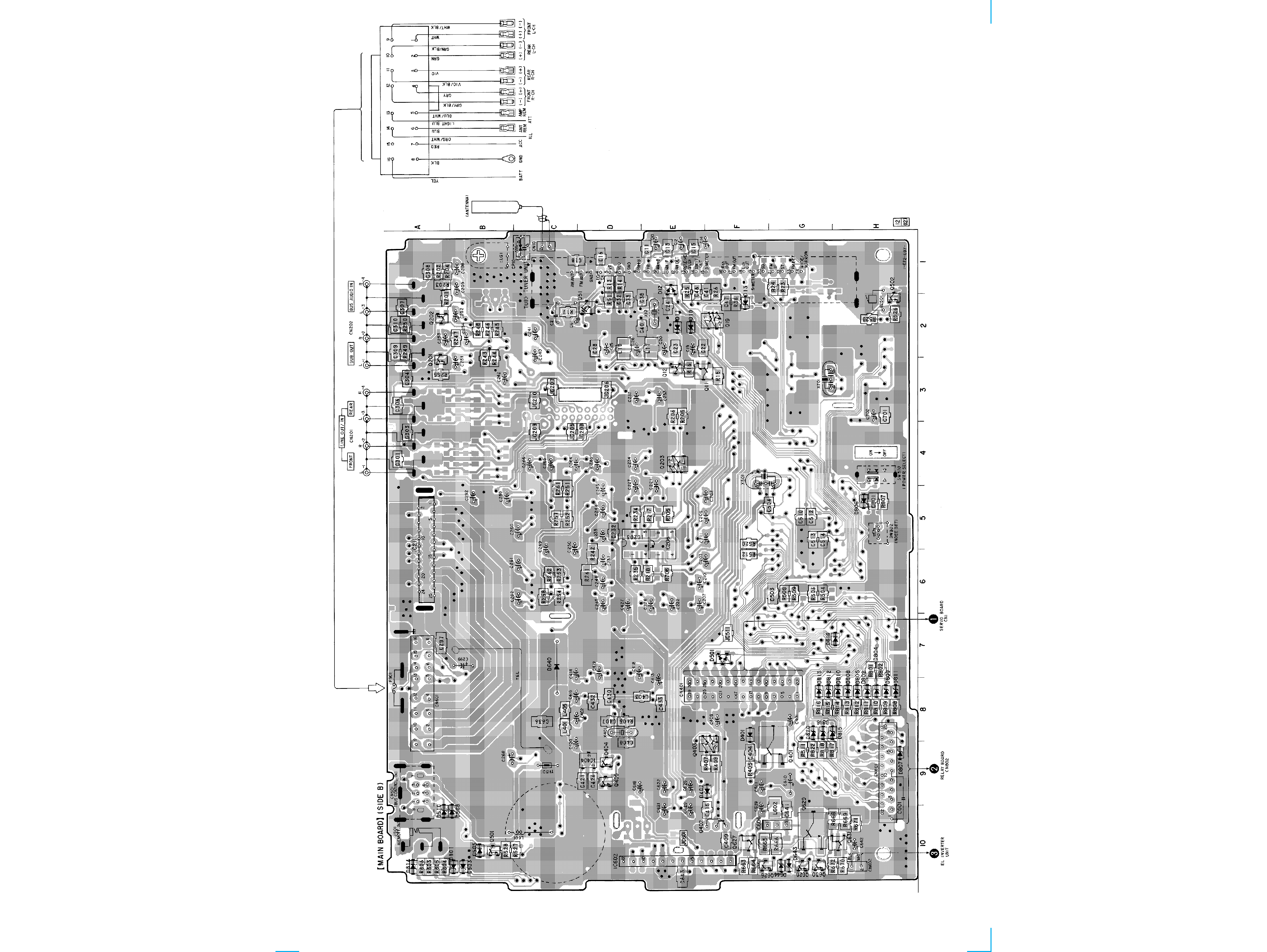
- RELAY BOARD - (SIDE A)
- MAIN BOARD - (SIDE A)
Main board Part No.
Former : 1-672-697-11
New
: 1-672-697-12
Relay board Part No.
Former : 1-672-698-11
New
: 1-672-698-12
2
For schematic diagrams
· All capacitors are in µF unless otherwise noted. pF: µµF
50 WV or less are not indicated except for electrolytics
and tantalums.
· All resistors are in
and 1/4 W or less unless otherwise
specified.
·
%
: indicates tolerance.
·
¢
: internal component.
· C : panel designation.
THIS NOTE IS COMMON FOR PRINTED WIRING BOARDS
AND SCHEMATIC DIAGRAMS.
(In addition to this, the necessary note is
printed in each block.)
· U : B+ Line.
· Power voltage is dc 14.4V and fed with regulated dc power
supply from ACC and BATT cords.
· Voltages are taken with a VOM (Input impedance 10 M
).
Voltage variations may be noted due to normal produc-
tion tolerances.
· Waveforms are taken with a oscilloscope.
Voltage variations may be noted due to normal produc-
tion tolerances.
· Circled numbers refer to waveforms.
· Signal path.
F
: FM
f
: AM
J
: CD
· ((
)) : Page of service manual.
<<
>> : Page of supplement-1.
For printed wiring boards
· X : parts extracted from the component side.
· Y : parts extracted from the conductor side.
·
r
: Through hole.
·
¢
: internal component.
· b : Pattern from the side which enables seeing.
(The other layer's patterns are not indicated.)
The components identified by
mark
! or dotted line with mark.
! are critical for safety.
Replace only with part number
specified.
Les composants identifiés par une
marque
! sont critiques pour la
sécurité.
Ne les remplacer que par une piéce
portant le numéro spécifié.
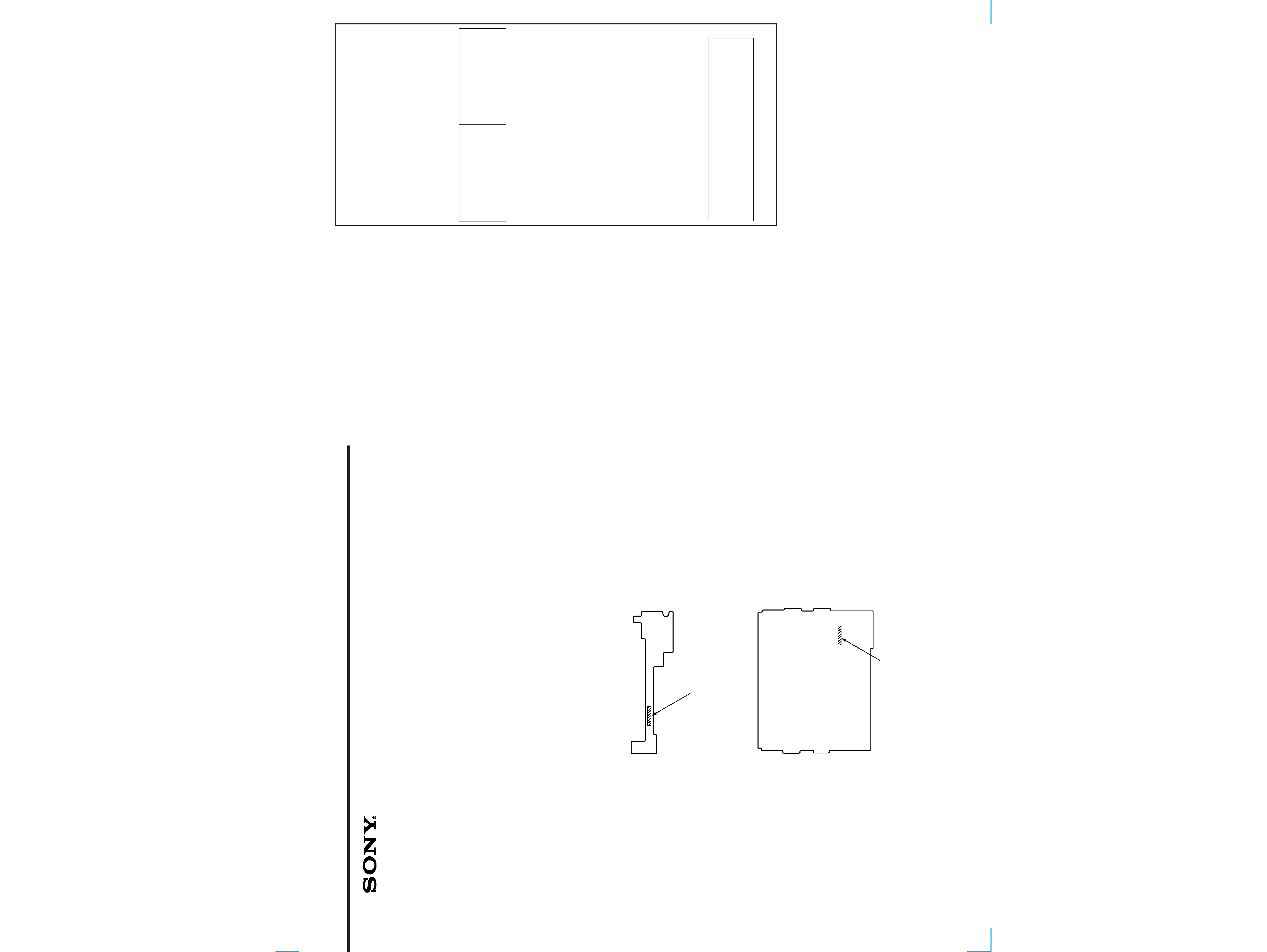
Caution:
Pattern face side: Parts on the pattern face side seen from the
(Side B)
pattern face are indicated.
Parts face side:
Parts on the parts face side seen from the
(Side A)
parts face are indicated.
· ((
)) : Page of service manual.
<<
>> : Page of supplement-1.
3
4
CDX-C7850
1. PRINTED WIRING BOARD -- MAIN SECTION --
(IC206)
E-5
IC207
C-5
IC208
C-6
(IC211)
A-6
IC401
D-8
IC403
D-7
(IC404)
D-9
IC501
G-5
IC505
B-10
IC601
G-10
(IC602)
D-10
IC604
G-10
(IC606)
G-10
IC701
H-3
IC702
G-3
(Q11)
F-3
(Q12)
E-3
Q14
G-1
Q15
G-1
Q16
E-1
Q17
F-1
Q18
F-1
(Q19)
F-2
(Q51)
D-2
(Q201)
A-3
(Q202)
A-2
(Q203)
E-4
Q205
C-8
Q206
C-8
Q207
C-4
Q208
B-4
Q209
D-4
Q210
D-4
Q211
C-8
Q212
B-3
Q213
B-3
Q214
B-4
Q215
B-4
(Q401)
G-9
(Q402)
F-10
(Q403)
E-9
(Q404)
D-9
(Q405)
D-9
(Q501)
B-10
(Q502)
H-1
Q503
A-10
Q504
B-10
Q508
B-9
Q604
B-8
Q608
B-8
Q611
G-9
Q612
H-8
Q617
H-8
Q619
H-9
Q621
H-8
Q622
C-8
Q623
H-8
Q624
H-7
Q625
H-7
(Q626)
F-10
(Q627)
F-10
(Q628)
G-10
(Q629)
G-9
(Q630)
G-10
(Q631)
H-10
Q801
H-10
Q802
H-10
(D10)
E-2
(D11)
E-2
(D12)
E-1
(D13)
F-2
D201
F-7
D202
C-7
D203
C-8
D204
B-5
D205
B-5
D206
B-5
D207
B-6
D208
B-6
D209
B-6
D210
B-6
D211
B-6
D212
C-7
(D401)
F-8
(D402)
E-9
(D501)
F-7
D502
H-6
(D505)
B-10
D506
B-10
D507
B-10
(D508)
B-10
D509
B-10
(D510)
A-10
D511
B-10
D602
B-8
D603
B-8
D605
G-10
D606
F-10
D607
B-8
D608
F-10
D609
B-8
D610
G-9
D621
B-7
D622
B-7
D637
B-7
(D640)
C-7
D642
H-8
(D643)
G-10
(D644)
G-10
(D801)
B-10
(D802)
H-8
(D803)
B-10
(D804)
H-8
(D805)
H-8
(D806)
H-5
(D807)
H-9
(D808)
H-8
(D809)
H-8
(D810)
H-8
(D811)
H-8
(D812)
G-8
(D813)
G-8
(D814)
A-10
(D815)
H-8
(D816)
G-8
(D818)
G-7
D819
H-10
(D820)
G-8
IC10
D-2
IC11
F-2
IC201
E-4
IC202
E-5
(IC203)
E-5
IC204
E-4
IC205
B-2
· Semiconductor Location
Ref. No.
Location
Ref. No.
Location
(
) : SIDE B
CDX-C7850
5
6
((Page 15))
((Page 16))
<<Page 45>>
7
8
CDX-C7850
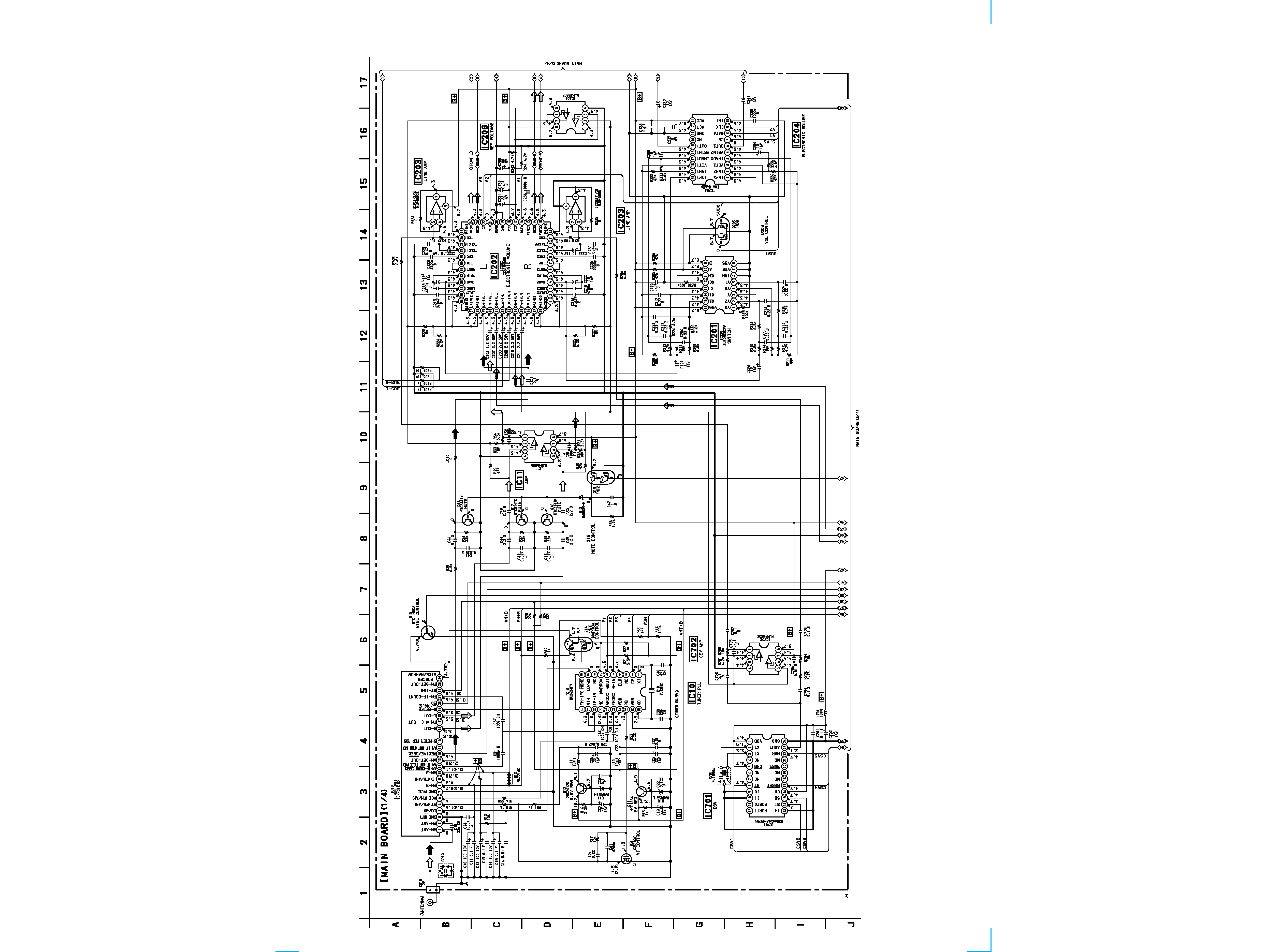
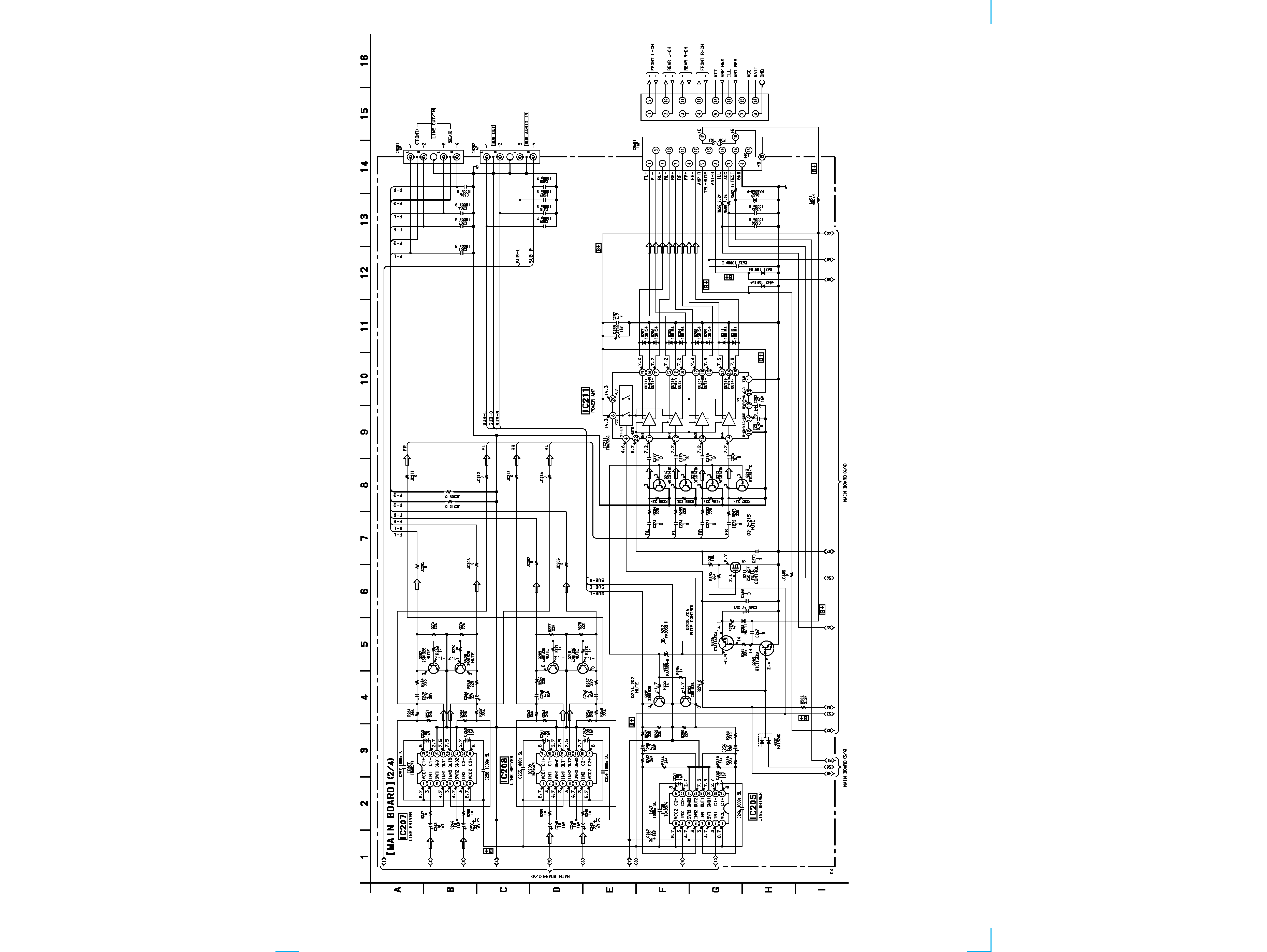
2. SCHEMATIC DIAGRAM -- MAIN SECTION (1/4) --
Note:
· Voltage is dc with respect to ground under
no-signal (detuned) condition.
no mark : FM
(
) : AM
((Page 12))
((P
age
9))
CDX-C7850
9
10
3. SCHEMATIC DIAGRAM -- MAIN SECTION (2/4) --
Note:
· Voltage is dc with respect to ground under
no-signal (detuned) condition.
no mark : FM
((P
age
8))
((Page 12))
((Page 13))