11
SERVICE MANUAL
E Model
CDX-3700
SUPPLEMENT-1
File this supplement with the service manual.
Subject : Change of Main and Key Boards
When performing service and inspection, check the suffix of the part number of
the main and key boards.
(ECN-CSB00629)
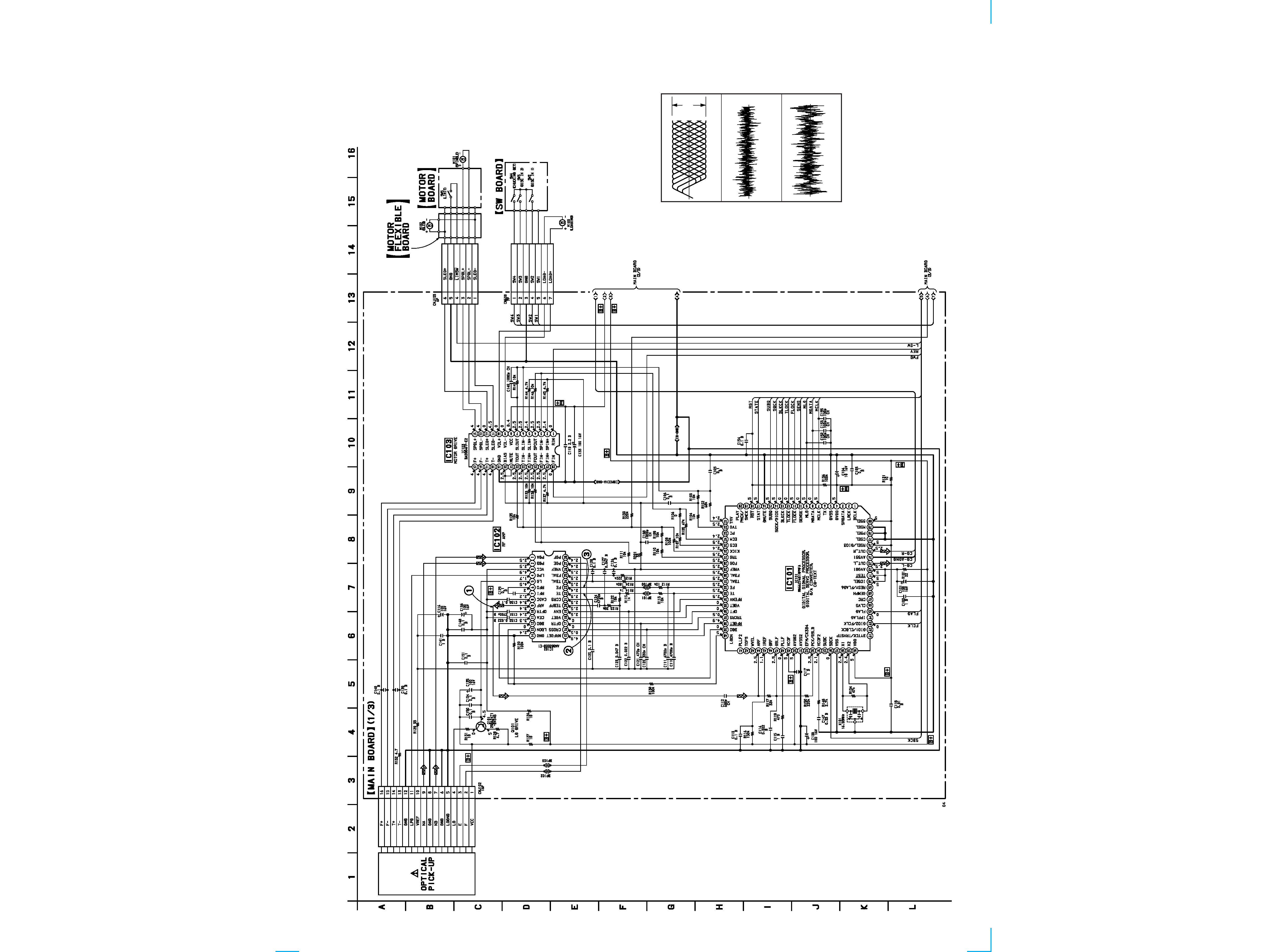
For schematic diagrams
· All capacitors are in µF unless otherwise noted. pF: µµF
50 WV or less are not indicated except for electrolytics
and tantalums.
· All resistors are in
and 1/4 W or less unless otherwise
specified.
·
%
: indicates tolerance.
·
¢
: internal component.
· C : panel designation.
THIS NOTE IS COMMON FOR PRINTED WIRING BOARDS
AND SCHEMATIC DIAGRAMS.
(In addition to this, the necessary note is
printed in each block.)
· U : B+ Line.
· Power voltage is dc 14.4V and fed with regulated dc power
supply from ACC and BATT cords.
· Voltages are taken with a VOM (Input impedance 10 M
).
Voltage variations may be noted due to normal produc-
tion tolerances.
· Waveforms are taken with a oscilloscope.
Voltage variations may be noted due to normal produc-
tion tolerances.
· Circled numbers refer to waveforms.
· Signal path.
F
: FM
f
: AM
J
: CD
· ((
)) : Page of supplement-1.
For printed wiring boards
· Y : parts extracted from the conductor side.
·
®
: Through hole.
·
¢
: internal component.
· b : Pattern from the side which enables seeing.
(The other layer's patterns are not indicated.)
· ((
)) : Page of supplement-1.
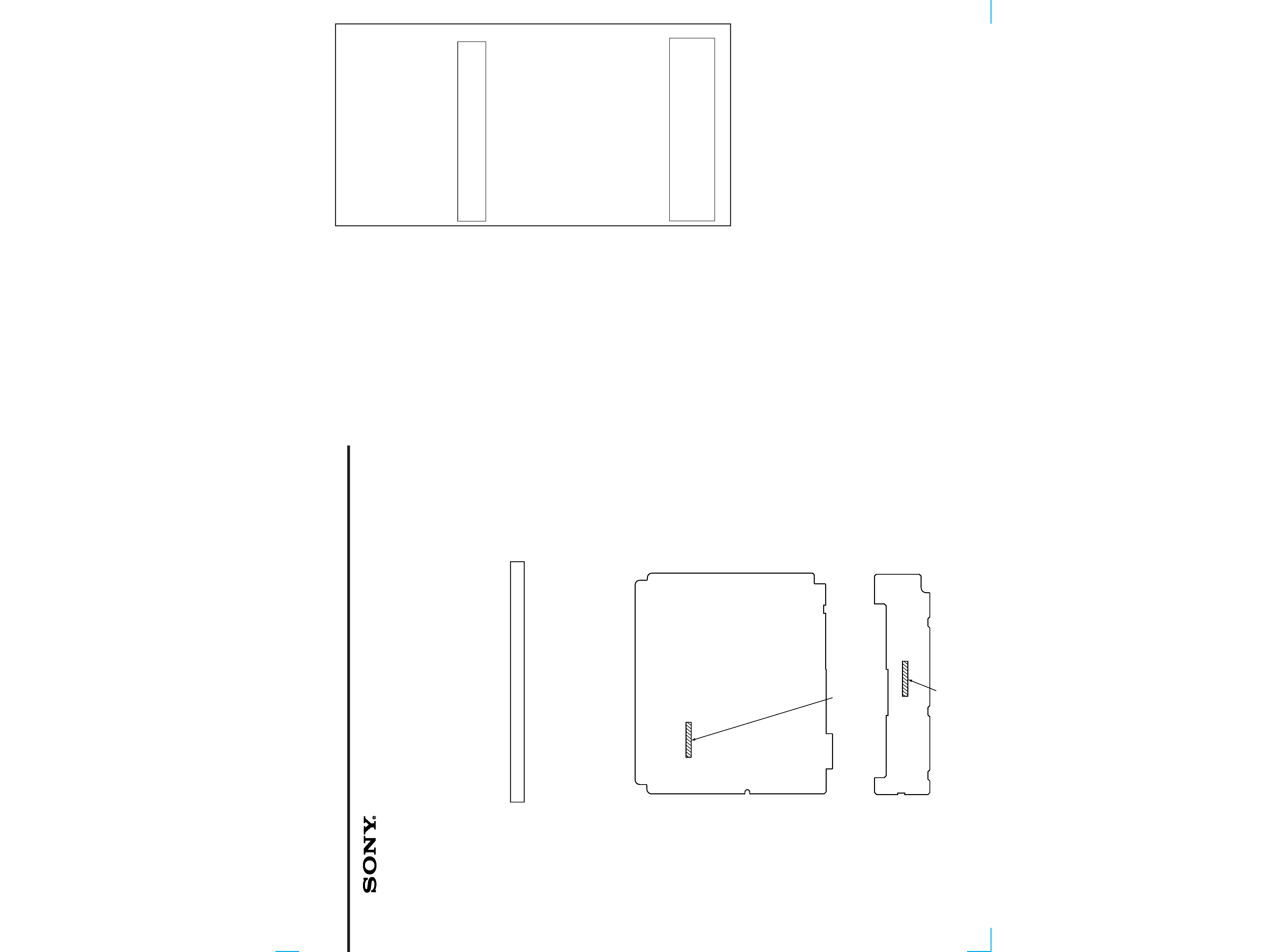
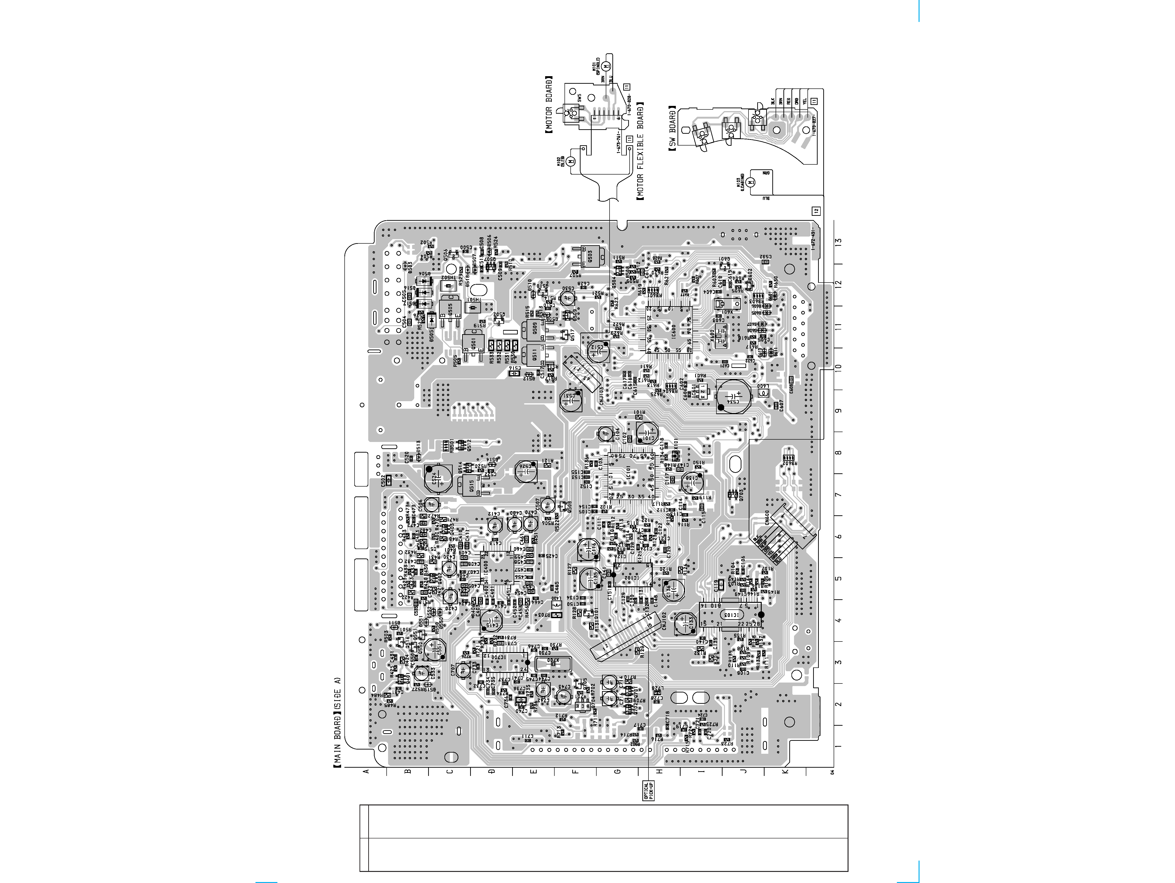
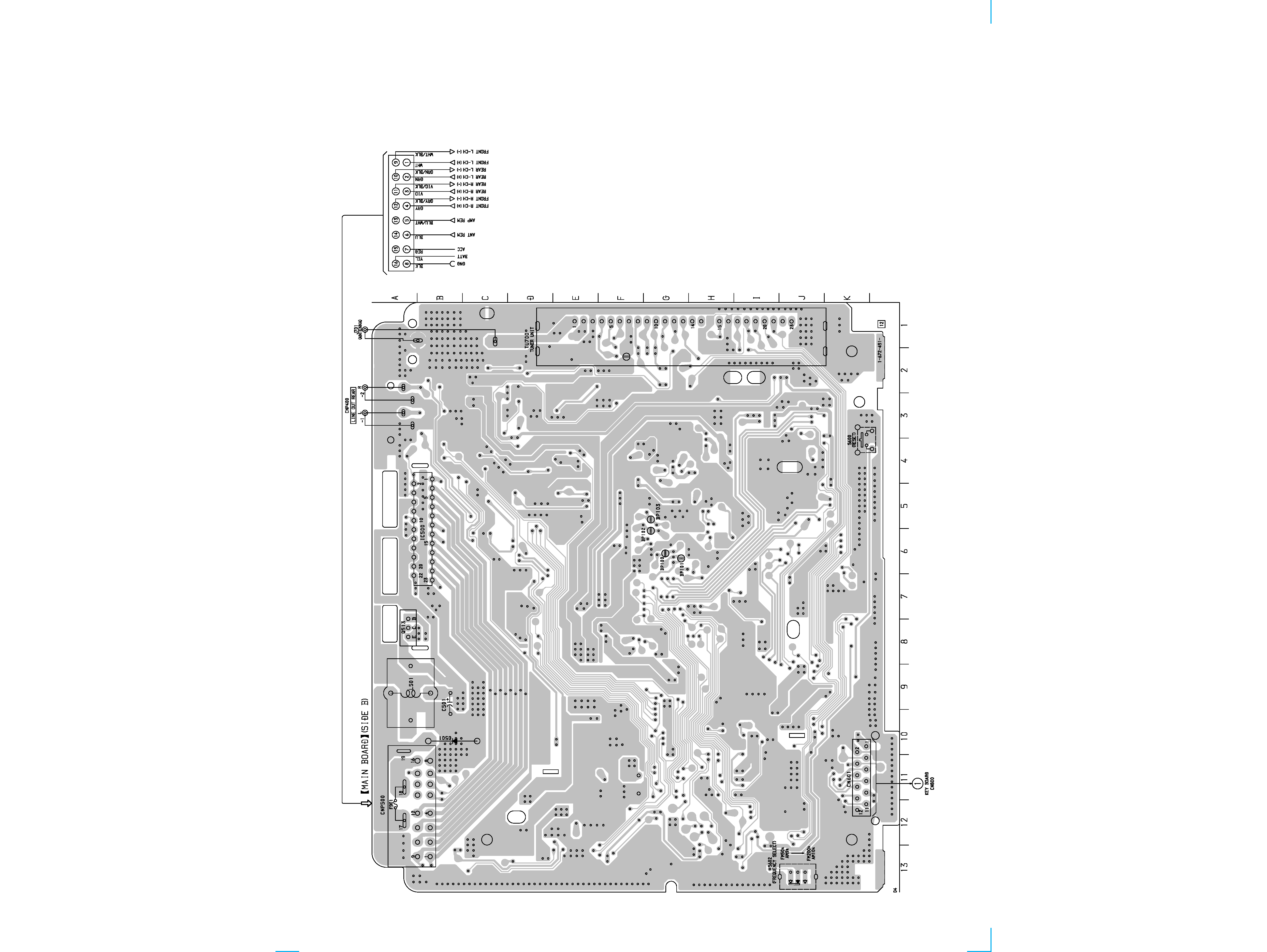
MAIN BOARD (SIDE B)
MAIN Board Part No.
Former : 1-672-491-11
New
: 1-672-491-12
KEY Board Part No.
Former : 1-672-492-11
New
: 1-672-492-12
KEY BOARD (SIDE B)
Note: The components identified by mark
! or dotted line
with mark
! are critical for safety.
Replace only with part number specified.
Caution:
Pattern face side: Parts on the pattern face side seen from the
(Side B)
pattern face are indicated.
Parts face side:
Parts on the parts face side seen from the
(Side A)
parts face are indicated.
1. DISCRIMINATION
22
CDX-3700
2. PRINTED WIRING BOARDS -- MAIN SECTION --
(LIMIT)
SW3
(DISC IN 2)
SW2
(DISC IN 1)
SW4
CHUCKING
DET
(
)
-
+
-
+
-
+
Ref. No.
Location
(D501)
B-10
D503
B-13
D504
B-12
D505
C-11
D506
D-13
D507
D-12
D508
E-11
D509
F-11
D510
E-12
D511
B-4
D512
E-10
D513
B-8
D514
D-8
D516
B-12
D517
B-12
D518
C-12
D519
C-2
D550
C-4
D551
B-4
D552
C-4
D601
K-12
D602
J-12
D605
J-11
D606
J-11
D607
J-11
D608
J-11
D610
J-10
D611
K-10
IC101
G-8
IC102
G-5
IC103
J-4
IC400
D-5
(IC500)
B-6
IC600
H-11
IC601
I-9
IC700
D-3
Q101
F-4
Q401
B-3
Q402
C-5
Q403
C-6
Q501
D-11
Q502
D-11
Q503
F-13
Q504
G-12
Q505
C-11
Q506
C-13
Q507
D-13
Q508
F-7
Q509
E-11
Q510
E-12
Q511
E-10
Q512
C-8
(Q513)
A-8
Q514
C-8
Q515
D-7
Q516
B-3
Q517
F-11
Q550
B-3
Q551
B-4
Q601
J-13
Q701
G-2
Q702
G-2
Q703
J-7
Q704
F-2
Q705
F-3
· Semiconductor
Location
(
) : SIDE B
33
CDX-3700
((Page 8))
44
CDX-3700
3. SCHEMATIC DIAGRAM -- MAIN SECTION (1/3) --
Note:
· Voltage and waveforms are dc with respect
to ground under no-signal conditions.
no mark : CD PLAY
((Page 5))
((Page 6))
· Waveforms
(MODE:PLAY)
3
1
2
Approx. 600mVp-p
IC102
@£ (FE)
0V
IC102
9 (ARF)
1.3Vp-p
Approx. 200mVp-p
IC102
@TM (TE)
0V
55
CDX-3700
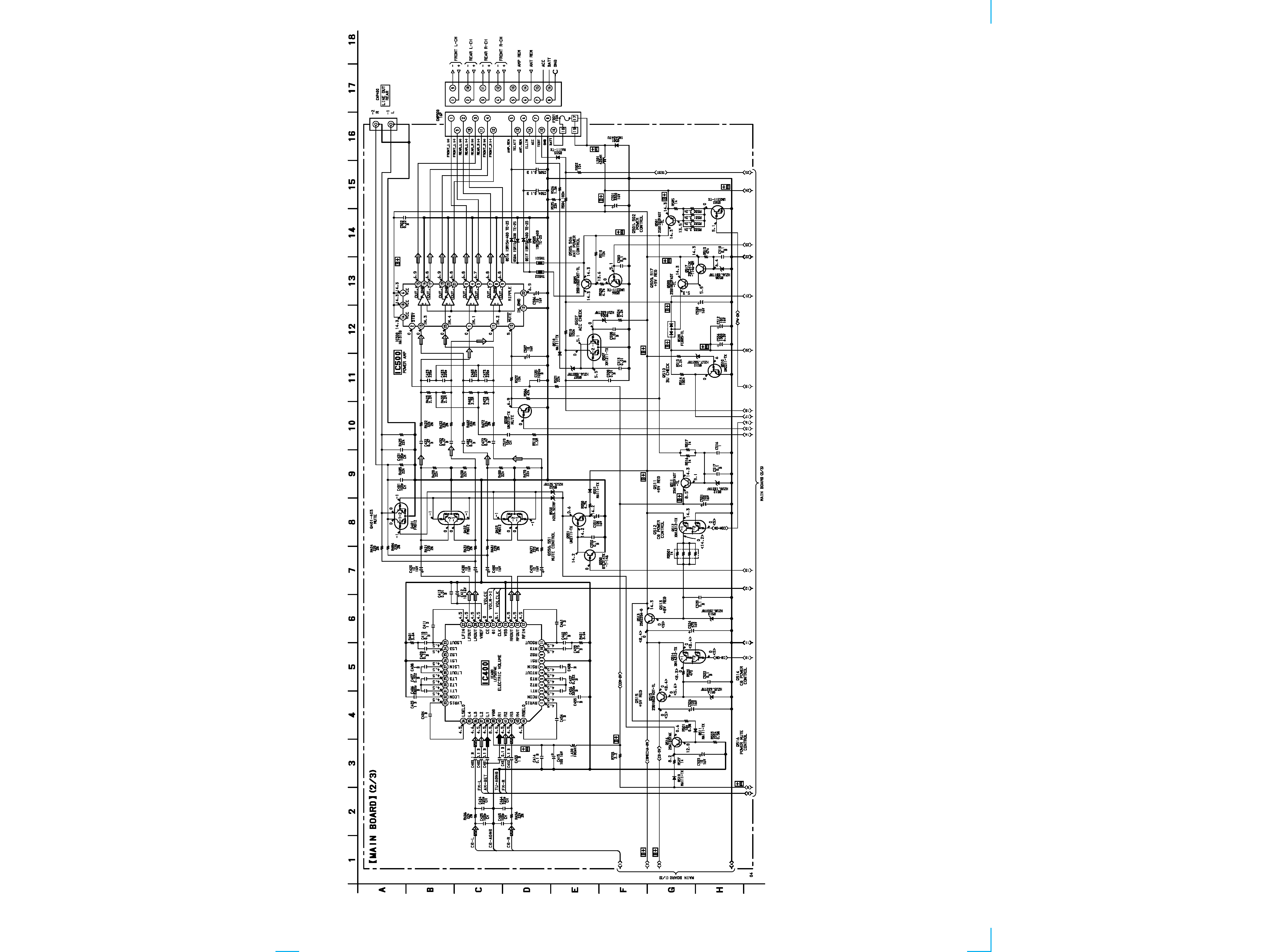
4. SCHEMATIC DIAGRAM -- MAIN SECTION (2/3) --
Note:
· Voltage is dc with respect to ground under no-signal
(detuned) condition.
no mark : FM
<
> : CD PLAY
((P
age
4))
((Page 6))