ORDER NO.
PIONEER CORPORATION 4-1, Meguro 1-chome, Meguro-ku, Tokyo 153-8654, Japan
PIONEER ELECTRONICS SERVICE, INC. P.O. Box 1760, Long Beach, CA 90801-1760, U.S.A.
PIONEER EUROPE NV Haven 1087, Keetberglaan 1, 9120 Melsele, Belgium
PIONEER ELECTRONICS ASIACENTRE PTE. LTD. 253 Alexandra Road, #04-01, Singapore 159936
PIONEER CORPORATION 2001
RRV2458
T ZZK MAY 2001 Printed in Japan
THIS MANUAL IS APPLICABLE TO THE FOLLOWING MODEL(S) AND TYPE(S).
Model No.
Order No.
Remarks
VSX-D810S/KUXJI
RRV2431
¶ This service manual should be used together with the following manual(s):
AUDIO/VIDEO MULTI-CHANNEL RECEIVER
VSX-D850S
CONTENTS
1. CONTRAST OF MISCELLANEOUS PARTS ........ 2
2. SCHEMATIC DIAGRAM ....................................... 5
Type
Model
Power Requirement
Remarks
VSX-D850S
KUXJI/CA
AC120V
VSX-D850S
2
1. CONTRAST OF MISCELLANEOUS PARTS
CONTRAST TABLE
Parts marked by "NSP" are generally unavailable because they are not in our Master Spare Parts List.
The
mark found on some component parts indicates the importance of the safety factor of the part.
Therefore, when replacing, be sure to use parts of identical designation.
Screws adjacent to
mark on product are used for disassembly.
Reference Nos. indicate the pages and Nos. in the service manual for the base model.
NOTES:
When ordering resistors, first convert resistance values into code form as shown in the following examples.
Ex.1 When there are 2 effective digits (any digit apart from 0), such as 560 ohm and 47k ohm (tolerance is shown by J=5%,
and K=10%).
Ex.2 When there are 3 effective digits (such as in high precision metal film resistors).
561
473
R50
1R0
5621
560
47k
0.5
1
RD1/4PU
J
RD1/4PU
J
RN2H
K
RS1P
K
56 x 101
47 x 103
R50
1R0
561
473
5.62k
RN1/4PC
F
562 x 101
5621
VSX-D850S/KUXJI/CA and VSX-D810S/KUXJI are constructed the same except for the following :
Part No.
Ref. No. Mark
Symbol and Description
VSX-D810S
VSX-D850S
Remarks
/KUXJI
/KUXJI/CA
PCB ASSEMBLIES
D.D & INPUT ASSY
XWK3027
XWK3029
P5- 1
D.D UCOM ASSY
XWZ3397
XWZ3399
P5-53
D.D DSP ASSY
XWZ3395
XWZ3396
NSP
AMP&PS ASSY
XWK3023
XWK3026
P5- 2
AMP&PRIMARY ASSY
XWZ3380
XWZ3383
NSP
COMPLEX ASSY
XWK3010
XWK3014
P5- 6
VIDEO&6CH IN ASSY
XWZ3335
XWZ3400
P5- 7
6CH IN ASSY
XWZ3350
XWZ3351
P5- 8
S. VISEO ASSY
XWZ3363
XWZ3364
P5- 9
COMPONENT ASSY
XWZ3366
XWZ3367
P6- 1
FRONT ASSY
XWZ3345
XWZ3349
P6- 3
R. ENCODER ASSY
XWZ3354
XWZ3355
PACKING SECTION
P3- 4
NSP
Dry Cell Battery (R6P, AA)
VEM-013
Not used
P3- 4
NSP
Alkaline Dry Cell Battery (LR6, AA)
Not used
VEM1021
P3- 6
Operating Instructions (French)
Not used
XRC3030
P3- 7
Remote Control Unit
XXD3028
XXD3031
P3-13
Packing Case
XHD3147
XHD3148
EXTERIOR SECTION
P5-37
Foot Assy
REC1263
Not used
P5-37
Insulator
Not used
PNW2766
P5-39
Rear Panel
XNC3077
XNC3078
FRONT PANEL SECTION
P6-18
Display Panel
XAK3172
XAK3216
P6-19
Button Cover
XAK3253
XAK3224
P6-21
Front Panel
XMB3033
XMB3034
B Lens R4
Not used
XAK3181
No. 1
Notes :
÷The numbers in the remarks column correspond to the numbers on the " EXPLODED VIEWS ".
÷ For PCB ASSEMBLIES, Refer to "CONTRAST OF PCB ASSEMBLIES" and "2. SCHEMATIC DIAGRAM".
VSX-D850S
3
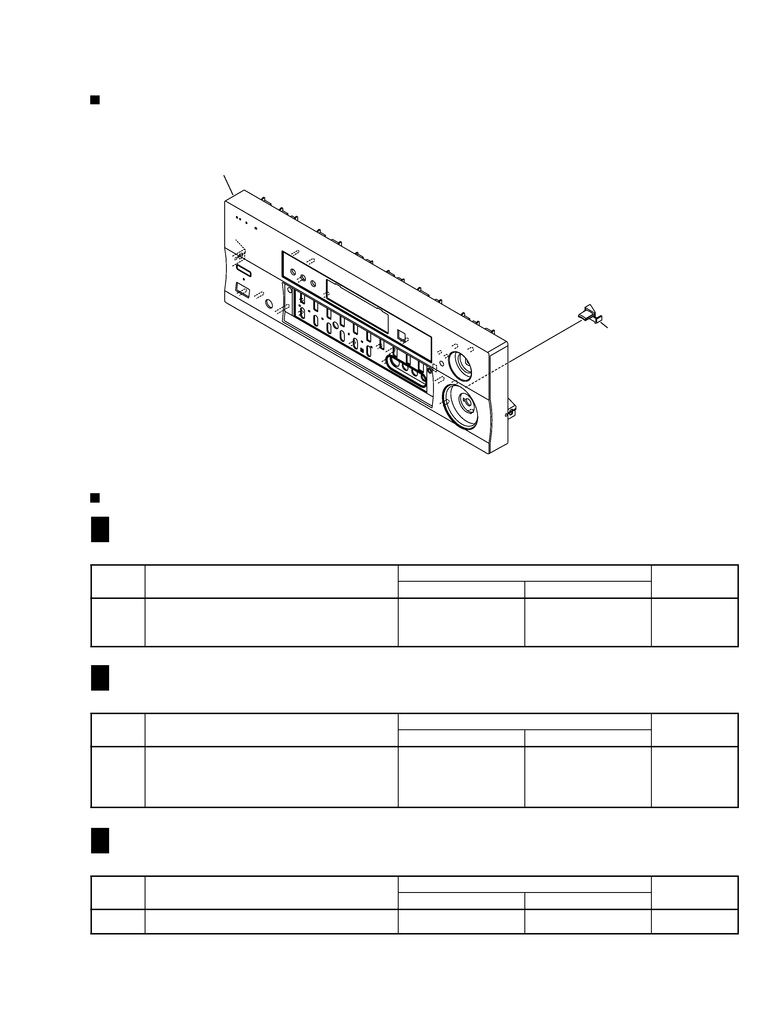
EXPLODED VIEWS
÷ FRONT PANEL SECTION
CONTRAST OF PCB ASSEMBLIES
D.D UCOM ASSY
XWZ3399 and XWZ3397 are constructed the same except for the following :
Mark
Symbol and Description
Part No.
Remarks
XWZ3397
XWZ3399
R153, R154, R159, R160
RS1/16S102J
RS1/16S911J
R165, R208
RS1/16S182J
RS1/16S162J
R189, R190, R197, R198
RS1/16S242J
RS1/16S222J
JA101JA104 (4P PIN JACK)
AKB7048
AKB7108
D.D DSP ASSY
XWZ3396 and XWZ3395 are constructed the same except for the following :
Mark
Symbol and Description
Part No.
Remarks
XWZ3395
XWZ3396
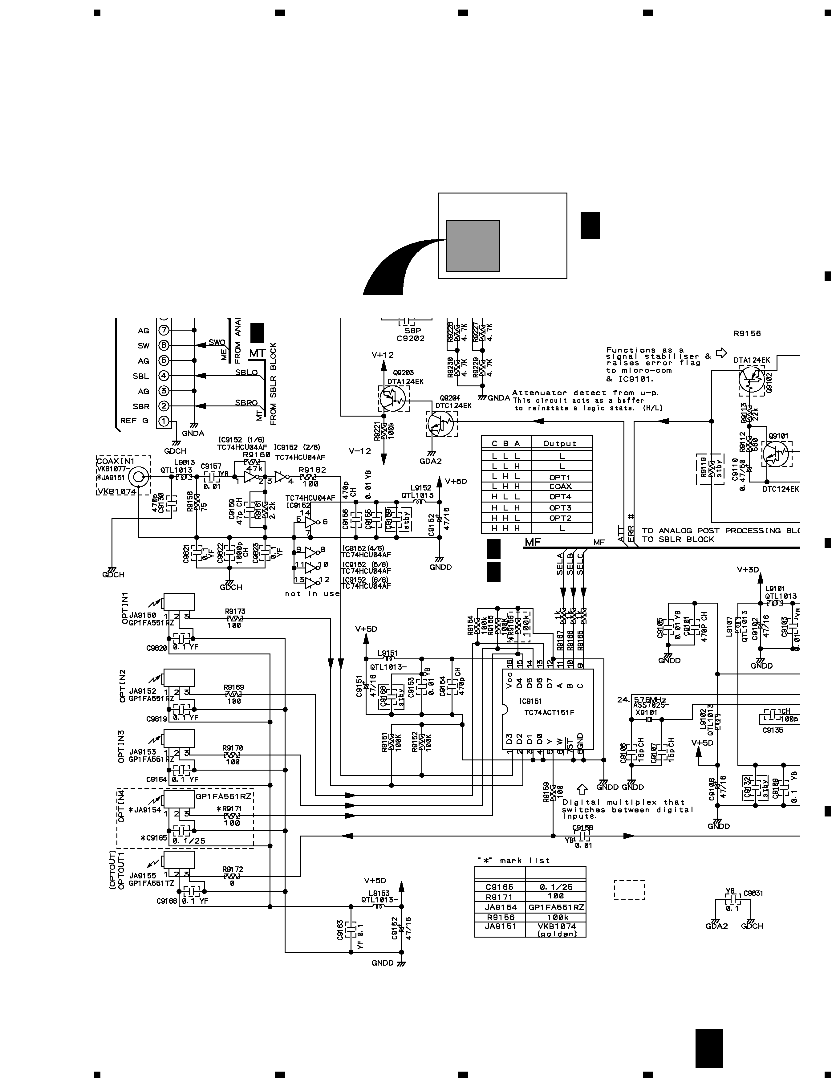
C9165
Not used
CKSRYF104Z25
R9156
RS1/16S0R0J
RS1/16S104J
R9171
Not used
RS1/16S101J
JA9151 (1P PIN JACK)
VKB1077
VKB1074
JA9154 (OPTICAL LINK IN)
Not used
GP1FA551RZ
F
A
F
B
AMP&PRIMARY ASSY
XWZ3383 and XWZ3380 are constructed the same except for the following :
Mark
Symbol and Description
Part No.
Remarks
XWZ3380
XWZ3383
C701, C702 (4700
µF/71V)
ACH7137
Not used
C701, C702 (5600
µF/71V)
Not used
XCH3005
F
C
Front Panel
1
VSX-D850S
4
FRONT ASSY
XWZ3349 and XWZ3345 are constructed the same except for the following :
F
N
COMPONENT ASSY
XWZ3367 and XWZ3366 are constructed the same except for the following :
Mark
Symbol and Description
Part No.
Remarks
XWZ3366
XWZ3367
1575 (6P PINJACK)
AKB7089
AKB7088
JA551 (6P RCA PINJACK)
AKB7128
AKB7127
JA553 (3P RCA PINJACK)
AKB7124
XKB3015
R.ENCODER ASSY
XWZ3355 and XWZ3354 are constructed the same except for the following :
F
M
F
O
Mark
Symbol and Description
Part No.
Remarks
XWZ3335
XWZ3400
CN305 (6P PINJACK)
AKB7123
XKB3014
Mark
Symbol and Description
Part No.
Remarks
XWZ3345
XWZ3349
R428
Not used
RS1/16S472J
R429
RS1/16S0R0J
RS1/16S622J
Mark
Symbol and Description
Part No.
Remarks
XWZ3354
XWZ3355
D511
Not used
UDZS5.6B
D512
Not used
E1L4E-7B1A(2345)
R512
Not used
RS1/16S391J
512 (LED HOLDER)
Not used
XAK3154
VIDEO&6CH IN ASSY
XWZ3400 and XWZ3335 are constructed the same except for the following :
F
Q
Mark
Symbol and Description
Part No.
Remarks
XWZ3350
XWZ3351
308 (6P PINJACK)
AKB7089
AKB7088
6CH IN ASSY
XWZ3351 and XWZ3350 are constructed the same except for the following :
F
S
S. VIDEO ASSY
XWZ3364 and XWZ3363 are constructed the same except for the following :
F
T
Mark
Symbol and Description
Part No.
Remarks
XWZ3363
XWZ3364
CN352/JA352 (3-4P MINI DIN SOCKET)
XKP3045
AKP7049
CN353 (2-4P MINI DIN SOCKET)
XKP3044
AKP7023
VSX-D850S
5
A
B
C
D
1
23
4
1
2
3
4
2/4F
B
2. SCHEMATIC DIAGRAM
2.1 D.D DSP ASSY (2/4)
Note : When ordering service parts, be sure to refer to "EXPLODED VIEWS and PARTS LIST" or "PCB PARTS LIST"
VSX-D850S
different parts
B 1/4
B 1/4
B 3/4
D.D DSP ASSY
(XWZ3396)
B 2/4 F