ORDER NO.
PIONEER ELECTRONIC CORPORATION 4-1, Meguro 1-Chome, Meguro-ku, Tokyo 153-8654, Japan
PIONEER ELECTRONICS SERVICE, INC. P.O. Box 1760, Long Beach, CA 90801-1760, U.S.A.
PIONEER ELECTRONIC (EUROPE) N.V. Haven 1087, Keetberglaan 1, 9120 Melsele, Belgium
PIONEER ELECTRONICS ASIACENTRE PTE. LTD. 501 Orchard Road, #10-00 Wheelock Place, Singapore 238880
PIONEER ELECTRONIC CORPORATION 1998
RRV2020
T ZZK SEPT. 1998 Printed in Japan
CONTENTS
1. CONTRAST OF MISCELLANEOUS PARTS ........ 2
2. SCHEMATIC DIAGRAM ....................................... 5
3. PCB CONNECTION DIAGRAM .......................... 11
¶ Refer to the service manual RRV1769 for VSX-806RDS/HYXJI.
THHYANUAL IS APPLICABLE TO THE FOLLOWING MODEL(S) AND TYPE(S).
Model
VSX-708RDS
Type
Power Requirement
The voltage can be converted by
the following method.
HYXJI
HYXJIGR
AUDIO/VIDEO MULTI-CHANNEL RECEIVER
VSX-708RDS
AC220 230V
AC220 230V
:Alter the wiring of the Power-supply block at the primary winding of Power-transformer referring to the "Line Voltage Selection" described
in Service Manual.
AC240V
AC240V
VSX-708RDS
2
1. CONTRAST OF MISCELLANEOUS PARTS
Parts marked by "NSP" are generally unavailable because they are not in our Master Spare Parts List.
The
mark found on some component parts indicates the importance of the safety factor of the part.
Therefore, when replacing, be sure to use parts of identical designation.
Screws adjacent to
mark on product are used for disassembly.
Reference Nos. indicate the pages and Nos. in the service manual for the base model.
NOTES:
When ordering resistors, first convert resistance values into code form as shown in the following examples.
Ex.1 When there are 2 effective digits (any digit apart from 0), such as 560 ohm and 47k ohm (tolerance is shown by J=5%,
and K=10%).
Ex.2 When there are 3 effective digits (such as in high precision metal film resistors).
561
473
R50
1R0
5621
560
47k
0.5
1
RD1/4PU
J
RD1/4PU
J
RN2H
K
RS1P
K
56 x 101
47 x 103
R50
1R0
561
473
5.62k
RN1/4PC
F
562 x 101
5621
CONTRAST TABLE
VSX-708RDS/HYXJI, HYXJIGR and VSX-806RDS/HYXJI are constructed the same except for the following :
Notes:
÷ The numbers in the remarks column correspond to the numbers on "EXPLOEDED VIEWS".
÷ For ASSEMBLIES, refer to "CONTRAST OF PCB ASSEMBLIES" and "2. SCHEMATIC DIAGRAM".
.
f
e
R
.
o
N
k
r
a
Mn
o
i
t
p
i
r
c
s
e
D
d
n
a
l
o
b
m
y
S
.
o
N
t
r
a
P
s
k
r
a
m
e
R
S
D
R
6
0
8
-
X
S
V
I
J
X
Y
H
/
S
D
R
8
0
7
-
X
S
V
I
J
X
Y
H
/
S
D
R
8
0
7
-
X
S
V
R
G
I
J
X
Y
H
/
S
E
I
L
B
M
E
S
S
A
P
S
NY
S
S
A
X
E
L
P
M
O
C7
5
3
7
K
W
A3
9
4
7
K
W
A3
9
4
7
K
W
A
8
-
6
PY
S
S
A
R
S
/
O
E
D
I
V5
4
8
8
Z
W
A9
6
2
7
X
W
A9
6
2
7
X
W
A
9
-
6
PY
S
S
A
E
M
U
L
O
V4
4
8
8
Z
W
A8
6
2
7
X
W
A8
6
2
7
X
W
A
P
S
NY
S
S
A
P
M
A
C
R
&
T
N
O
R
F6
5
3
7
K
W
A4
9
4
7
K
W
A4
9
4
7
K
W
A
0
1
-
6
PY
S
S
A
R
E
K
A
E
P
S
C
/
R9
2
6
8
Z
W
A0
7
2
7
X
W
A0
7
2
7
X
W
A
3
-
7
PY
S
S
A
M
O
C
-
U
/
L
F5
2
6
8
Z
W
A1
9
2
7
X
W
A1
9
2
7
X
W
A
P
S
NY
S
S
A
N
I
H
C
6d
e
s
u
t
o
N8
8
4
7
K
W
A8
8
4
7
K
W
A1
.
o
N
G
N
I
K
C
A
P
3
-
3
Ps
n
o
i
t
c
u
r
t
s
n
I
g
n
i
t
a
r
e
p
O0
0
1
7
E
R
Ad
e
s
u
t
o
Nd
e
s
u
t
o
N
)
n
a
il
a
t
I
/
n
a
m
r
e
G
/
h
c
n
e
r
F
/
h
s
il
g
n
E
(
)
h
c
n
e
r
F
/
h
s
il
g
n
E
(
s
n
o
i
t
c
u
r
t
s
n
I
g
n
i
t
a
r
e
p
Od
e
s
u
t
o
N6
8
1
7
E
R
Ad
e
s
u
t
o
N
)
n
a
m
r
e
G
(
s
n
o
i
t
c
u
r
t
s
n
I
g
n
i
t
a
r
e
p
Od
e
s
u
t
o
Nd
e
s
u
t
o
N9
0
2
7
C
R
A
5
-
3
PP
S
Nd
r
a
C
y
t
n
a
r
r
a
W9
0
0
7
Y
R
A2
2
0
7
Y
R
A2
2
0
7
Y
R
A
8
-
3
Ps
n
o
i
t
c
u
r
t
s
n
I
g
n
i
t
a
r
e
p
O3
6
1
7
C
R
Ad
e
s
u
t
o
Nd
e
s
u
t
o
N
)
e
s
e
u
g
u
t
r
o
P
/
h
s
i
n
a
p
S
/
h
s
i
d
e
w
S
/
h
c
t
u
D
(
)
h
s
i
n
a
p
S
/
n
a
il
a
t
I
/
n
a
m
r
e
G
(
s
n
o
i
t
c
u
r
t
s
n
I
g
n
i
t
a
r
e
p
Od
e
s
u
t
o
N8
0
2
7
C
R
Ad
e
s
u
t
o
N
)
e
s
e
u
g
u
t
r
o
P
/
h
s
i
d
e
w
S
/
h
c
t
u
D
(
s
n
o
i
t
c
u
r
t
s
n
I
g
n
i
t
a
r
e
p
Od
e
s
u
t
o
N5
2
2
7
C
R
Ad
e
s
u
t
o
N
9
-
3
P)
8
1
1
X
S
V
-
U
C
(
t
i
n
U
l
o
r
t
n
o
C
e
t
o
m
e
R9
2
1
7
D
X
Ad
e
s
u
t
o
Nd
e
s
u
t
o
N
9
-
3
P)
3
4
1
X
S
V
-
U
C
(
t
i
n
U
l
o
r
t
n
o
C
e
t
o
m
e
Rd
e
s
u
t
o
N4
8
1
7
D
X
A4
8
1
7
D
X
A
2
1
-
3
Pe
s
a
C
g
n
i
k
c
a
P5
0
4
7
D
H
A4
5
6
7
D
H
A4
5
6
7
D
H
A
R
O
I
R
E
T
X
E
1
2
-
6
Pr
o
t
a
l
u
s
n
I2
1
9
1
W
N
P6
6
7
2
W
N
P6
6
7
2
W
N
P
3
2
-
6
Pl
e
n
a
P
r
a
e
R7
3
5
7
C
N
A8
2
7
7
C
N
A8
2
7
7
C
N
A
2
4
-
6
Pe
t
a
l
P
e
m
a
N8
0
6
1
M
A
P6
7
7
1
M
A
P6
7
7
1
M
A
P
P
S
Nr
e
c
a
p
Sd
e
s
u
t
o
N2
9
0
7
B
E
A2
9
0
7
B
E
A2
.
o
N
N
O
I
T
C
E
S
L
E
N
A
P
T
N
O
R
F
0
1
-
7
Pl
e
n
a
P
L
F3
9
2
7
K
A
A9
0
6
7
K
A
A9
0
6
7
K
A
A
2
1
-
7
Pl
e
n
a
P
b
u
S7
2
0
7
P
A
A5
5
0
7
P
A
A5
5
0
7
P
A
A
3
1
-
7
Pl
e
n
a
P
t
n
o
r
F2
2
4
7
B
M
A4
5
5
7
B
M
A4
5
5
7
B
M
A
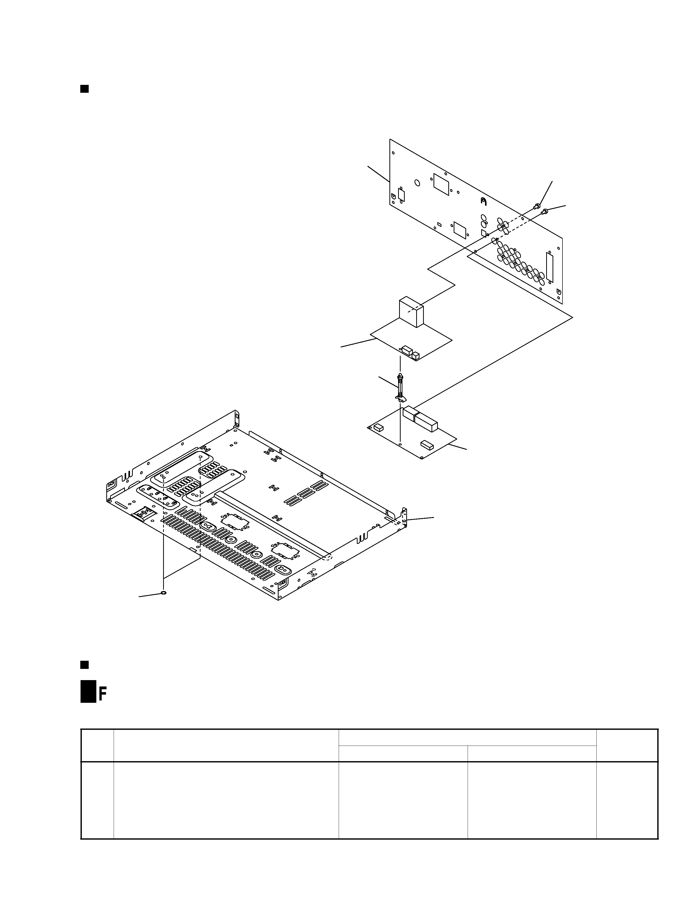
VSX-708RDS
3
No.2
Shassis
No.1
PCB Support
(AEC7056)
Rear Panel
Screw
BBZ30P080FZK
Screw
BBZ30P080FZK
VIDEO/SR ASSY
EXPLODED VIEWS
÷ EXTERIOR SECTION
CONTRAST OF PCB ASSEMBLIES
AWX7291 and AWZ8625 are constructed the same except for the following :
FL/U-COM ASSY
A
k
r
a
Mn
o
i
t
p
i
r
c
s
e
D
d
n
a
l
o
b
m
y
S
.
o
N
t
r
a
P
s
k
r
a
m
e
R
5
2
6
8
Z
W
A1
9
2
7
X
W
A
1
0
9
C
I
A
3
0
2
G
D
PA
3
3
2
G
D
P
2
5
9
Q
5
1
1
1
A
S
23
9
9
1
A
S
2
4
2
9
D
,
3
2
9
D
,
8
1
9
D
4
1
9
D
,
2
1
9
D
1
0
9
D
2
5
2
S
S
14
5
2
S
S
1
8
2
9
R
,
7
2
9
R
d
e
s
u
t
o
NJ
3
0
1
U
P
4
/
1
D
R
3
1
J
1
5
6
2
-
0
0
6
-
7
0
A
5
1
D1
5
6
2
-
0
0
6
-
0
1
A
5
1
D
VSX-708RDS
4
AWX7268 and AWZ8844 are constructed the same except for the following :
VOLUME ASSY
I
AWX7270 and AWZ8629 are constructed the same except for the following :
R/C SPEAKER ASSY
J
AWX7269 and AWZ8845 are constructed the same except for the following :
VIDEO/SR ASSY
L
k
r
a
Mn
o
i
t
p
i
r
c
s
e
D
d
n
a
l
o
b
m
y
S
.
o
N
t
r
a
P
s
k
r
a
m
e
R
4
4
8
8
Z
W
A8
6
2
7
X
W
A
6
0
7
Q
,
5
0
7
Q
5
1
1
1
A
S
23
9
9
1
A
S
2
5
0
7
D
,
3
0
7
D
,
1
0
7
D
2
5
2
S
S
14
5
2
S
S
1
0
1
7
C
,
9
0
7
C
0
5
K
1
5
1
B
Y
U
P
K
C0
5
J
0
8
6
L
S
U
P
C
C
3
1
7
C
d
e
s
u
t
o
N0
5
M
7
R
4
T
A
E
C
6
1
7
C
0
5
K
1
0
1
B
Y
U
P
K
C0
5
J
0
7
4
L
S
U
P
C
C
7
1
7
C
d
e
s
u
t
o
N0
5
M
0
2
2
T
A
E
C
1
6
0
9
C
,
0
6
0
9
C
d
e
s
u
t
o
N0
5
M
0
0
1
T
A
E
C
3
1
7
R
d
e
s
u
t
o
NJ
4
0
1
U
P
4
/
1
D
R
5
1
7
R
d
e
s
u
t
o
NJ
2
7
2
U
P
4
/
1
D
R
7
1
7
R
d
e
s
u
t
o
NJ
3
0
1
U
P
4
/
1
D
R
0
2
J
1
5
6
2
-
0
0
3
-
5
1
A
5
1
D1
5
6
2
-
0
0
4
-
5
1
A
5
1
D
k
r
a
Mn
o
i
t
p
i
r
c
s
e
D
d
n
a
l
o
b
m
y
S
.
o
N
t
r
a
P
s
k
r
a
m
e
R
9
2
6
8
Z
W
A0
7
2
7
X
W
A
4
5
1
D
1
5
1
D
2
5
2
S
S
14
5
2
S
S
1
6
5
1
R
J
1
5
7
U
P
4
/
1
D
RJ
2
2
1
U
P
4
/
1
D
R
9
7
1
R
d
e
s
u
t
o
NJ
2
7
2
U
P
4
/
1
D
R
k
r
a
Mn
o
i
t
p
i
r
c
s
e
D
d
n
a
l
o
b
m
y
S
.
o
N
t
r
a
P
s
k
r
a
m
e
R
5
4
8
8
Z
W
A9
6
2
7
X
W
A
3
5
8
D
1
5
8
D
,
2
0
8
D
,
1
0
8
D
2
5
2
S
S
14
5
2
S
S
1
2
0
8
N
C7
E
P
K0
1
E
P
K
4
2
J
d
e
s
u
t
o
N1
5
6
2
-
0
0
1
-
3
0
A
5
1
D
)
P
9
(
R
E
D
L
O
H
E
L
B
A
C
1
9
8
1
d
e
s
u
t
o
N5
0
9
0
-
3
6
0
1
5
SEMICONDUCTORS
IC101, IC102
NJM2058D
IC103, IC104
TC4053BP
D101, D102
MTZJ6.2B
CAPACITORS
C109C112
CEAT2R2M50
C119C122, C141, C142
CEAT470M16
C127C130, C135C138
CEAT4R7M50
C113, C114, C123C126
CGCYX473M25
C139, C140, C165
CGCYX473M25
C106C108
CKPUYB101K50
C144, C145
CKPUYB102K50
C115C118
CKPUYB331K50
C143
CKPUYB681K50
C101, C105
CKPUYF473Z16
RESISTORS
All Resistors
RD1/4PU
&&&J
OTHERS
102
15P CABLE HOLDER
51063-1505
CN103
PIN JACK(4P)
AKB7087
J20
JUMPER WIRE
D15A15-150-2651
CN101
CONNECTOR(15P)
KPE15
CN104
CONNECTOR(3P)
KPE3
PCB PARTS LIST
6CH IN ASSY
P
Mark No.
Description
Part No.
Mark No.
Description
Part No.
VSX-708RDS
5
A
B
C
D
1
23
4
1
2
3
4
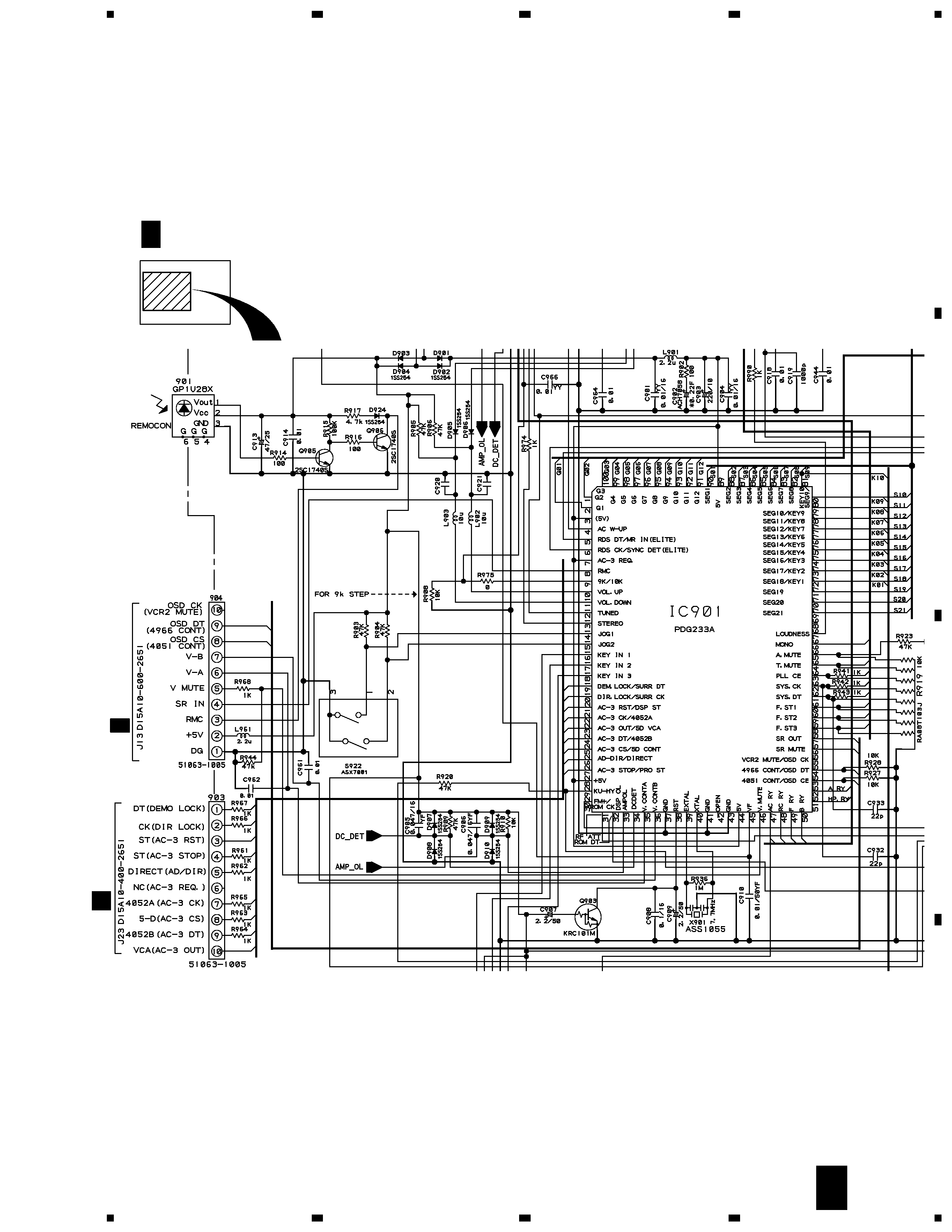
2. SCHEMATIC DIAGRAM
Note : When ordering service parts, be sure to refer to "EXPLODED VIEWS and PARTS LIST" or "PCB PARTS LIST"
2.1 FL/U-COM ASSY
F
A
L
CN802
H
CN3003
F
L
A F FL/U-COM ASSY (AWX7291)