ORDER NO.
PIONEER CORPORATION 4-1, Meguro 1-chome, Meguro-ku, Tokyo 153-8654, Japan
PIONEER ELECTRONICS (USA) INC. P.O. Box 1760, Long Beach, CA 90801-1760, U.S.A.
PIONEER EUROPE NV Haven 1087, Keetberglaan 1, 9120 Melsele, Belgium
PIONEER ELECTRONICS ASIACENTRE PTE. LTD. 253 Alexandra Road, #04-01, Singapore 159936
PIONEER CORPORATION 2008
2008 Printed in Japan
TIMER
DISPLAY OFF
STANDBY/ON
USB
SOUND RETRIEVER
PHONES
F. AUDIO IN
VOLUME
Z9
PDX-Z9
RRV3755
SUPER AUDIO CD RECEIVER
PDX-Z9
THIS MANUAL IS APPLICABLE TO THE FOLLOWING MODEL(S) AND TYPE(S).
Model
Type
Power Requirement
Remarks
PDX-Z9
WYVSXJ5
AC 220 V to 240 V
For details, refer to "Important Check Points for good servicing".
T-ZZV MAY
2
PDX-Z9
1
2
3
4
A
B
C
D
E
F
1
2
3
4
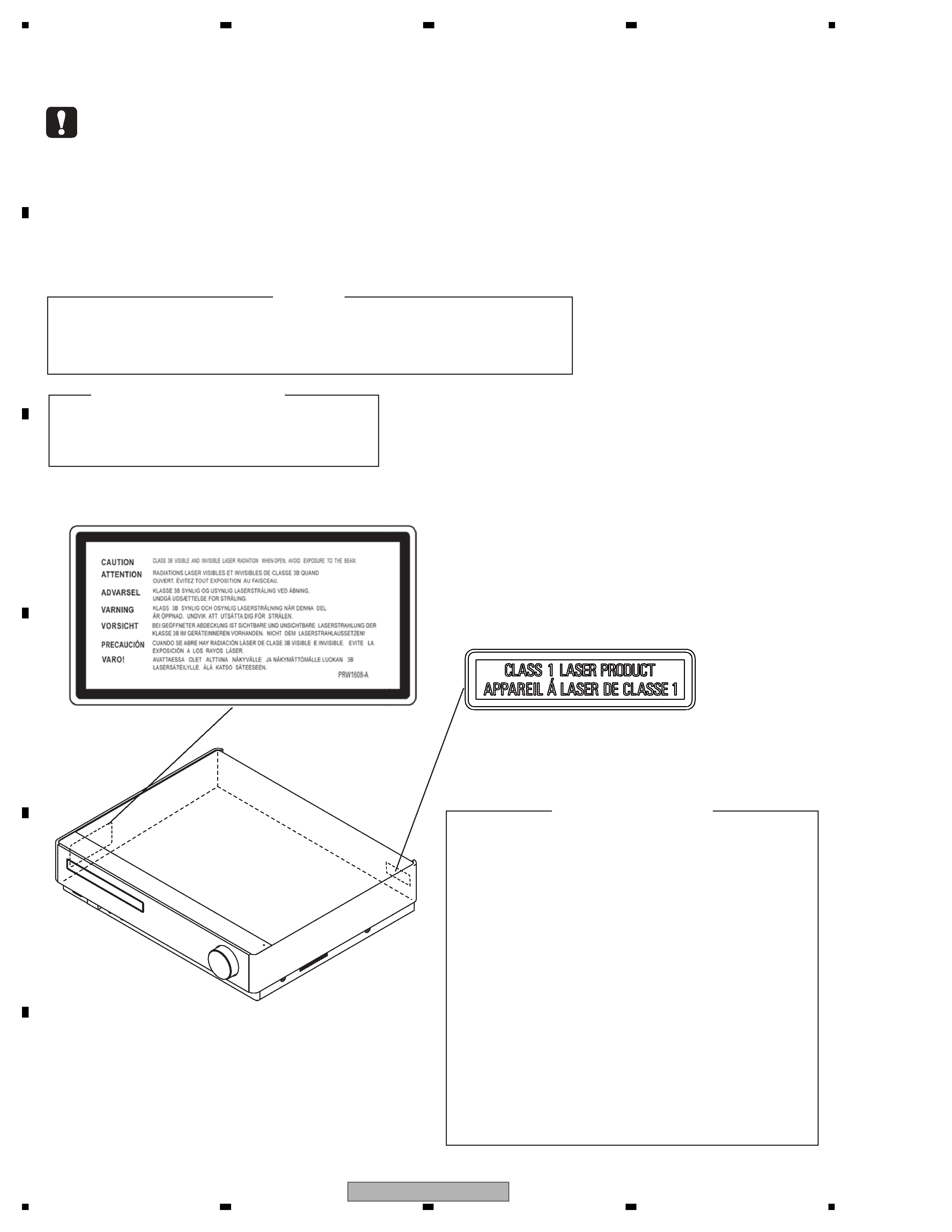
SAFETY INFORMATION
WARNING !
THE AEL (ACCESSIBLE EMISSION LEVEL) OF THE LASER POWER OUTPUT IS LESS THAN CLASS 1
BUT THE LASER COMPONENT IS CAPABLE OF EMITTING RADIATION EXCEEDING THE LIMIT FOR
CLASS 1.
A SPECIALLY INSTRUCTED PERSON SHOULD DO SERVICING OPERATION OF THE APPARATUS.
LASER DIODE CHARACTERISTICS
FOR CD :
MAXIMUM OUTPUT POWER : 7 mW Continuous
WAVELENGTH : 780 nm
FOR SACD :MAXIMUM OUTPUT POWER : 5 mW Continuous
WAVELENGTH : 650 nm
Additional Laser Caution
1. Laser Interlock Mechanism
· Loading switch (S101 on the LOAB Assy) is used for interlock
mechanism of the laser.
When this switch turned ON in SW2 (CLOSE) side (OPEN signal is
0V and CLOSE signal is 3.5V), a laser becomes the status which can
completely oscillation.
Furthermore, the laser completely oscillates in the disc judgment and
disc playback.
When player is power ON state and laser diode is not completely
oscillating, 780nm laser diode is always oscillating by half power.
· Laser diode is driving with Q307 (650nm LD) and Q308 (780nm LD)
on the DVDM Assy.
Therefore, when short-circuit between the emitter and collector of these
transistors or the base voltage is supplied for transistors turn on, the
laser oscillates. (failure mode)
· In the test mode *, there is the mode that the laser oscillates except
for the disc judgment and playback. LD ON mode in the test mode
oscillates with the laser forcibly.
The interlock mechanism mentioned above becomes invalid in this
mode.
2. When the cover is open, close viewing through the objective lens with
the naked eye will cause exposure to the laser beam.
LABEL CHECK
(Printed on the Rear Panel )
* : Refer to page 47.
PRW1608
This service manual is intended for qualified service technicians ; it is not meant for the casual
do-it-yourselfer. Qualified technicians have the necessary test equipment and tools, and have been
trainedto properly and safely repair complex products such as those covered by this manual.
Improperly performed repairs can adversely affect the safety and reliability of the product and may
void the warranty. If you are not qualified to perform the repair of this product properly and safely,
you should not risk trying to do so and refer the repair to a qualified service technician.
3
PDX-Z9
5
6
7
8
5
6
7
8
A
B
C
D
E
F
[Important Check Points for Good Servicing]
In this manual, procedures that must be performed during repairs are marked with the below symbol.
Please be sure to confirm and follow these procedures.
1. Product safety
Please conform to product regulations (such as safety and radiation regulations), and maintain a safe servicing environment by
following the safety instructions described in this manual.
1 Use specified parts for repair.
Use genuine parts. Be sure to use important parts for safety.
2 Do not perform modifications without proper instructions.
Please follow the specified safety methods when modification(addition/change of parts) is required due to interferences such as
radio/TV interference and foreign noise.
3 Make sure the soldering of repaired locations is properly performed.
When you solder while repairing, please be sure that there are no cold solder and other debris.
Soldering should be finished with the proper quantity. (Refer to the example)
4 Make sure the screws are tightly fastened.
Please be sure that all screws are fastened, and that there are no loose screws.
5 Make sure each connectors are correctly inserted.
Please be sure that all connectors are inserted, and that there are no imperfect insertion.
6 Make sure the wiring cables are set to their original state.
Please replace the wiring and cables to the original state after repairs.
In addition, be sure that there are no pinched wires, etc.
7 Make sure screws and soldering scraps do not remain inside the product.
Please check that neither solder debris nor screws remain inside the product.
8 There should be no semi-broken wires, scratches, melting, etc.on the coating of the power cord.
Damaged power cords may lead to fire accidents, so please be sure that there are no damages.
If you find a damaged power cord, please exchange it with a suitable one.
9 There should be no spark traces or similar marks on the power plug.
When spark traces or similar marks are found on the power supply plug, please check the connection and advise on secure
connections and suitable usage. Please exchange the power cord if necessary.
a Safe environment should be secured during servicing.
When you perform repairs, please pay attention to static electricity, furniture, household articles, etc. in order to prevent injuries.
Please pay attention to your surroundings and repair safely.
2. Adjustments
To keep the original performance of the products, optimum adjustments and confirmation of characteristics within specification.
Adjustments should be performed in accordance with the procedures/instructions described in this manual.
4. Cleaning
For parts that require cleaning, such as optical pickups, tape deck heads, lenses and mirrors used in projection monitors, proper
cleaning should be performed to restore their performances.
3. Lubricants, Glues, and Replacement parts
Use grease and adhesives that are equal to the specified substance.
Make sure the proper amount is applied.
5. Shipping mode and Shipping screws
To protect products from damages or failures during transit, the shipping mode should be set or the shipping screws should be
installed before shipment. Please be sure to follow this method especially if it is specified in this manual.

4
PDX-Z9
1
2
3
4
A
B
C
D
E
F
1
2
3
4
CONTENTS
SAFETY INFORMATION ..........................................................................................................................................................2
1. SERVICE PRECAUTIONS ....................................................................................................................................................5
1.1 NOTES ON SOLDERING ...............................................................................................................................................5
1.2 NOTES ON BTL DRIVE ..................................................................................................................................................5
2. SPECIFICATIONS .................................................................................................................................................................6
2.1 ACCESSORIES ..............................................................................................................................................................6
2.2 SPECIFICATIONS...........................................................................................................................................................6
2.3 DISC CONTENT FORMAT .............................................................................................................................................7
2.4 PANEL FACILITIES .........................................................................................................................................................8
3. BASIC ITEMS FOR SERVICING.........................................................................................................................................12
3.1 CHECK POINTS AFTER SERVICING..........................................................................................................................12
3.2 PCB LOCATIONS .........................................................................................................................................................13
3.3 JIGS LIST (INCLUDE GREASE) ..................................................................................................................................14
4. BLOCK DIAGRAM...............................................................................................................................................................16
4.1 LOAB ASSY and OVERALL WIRING DIAGRAM .........................................................................................................16
4.2 OVERALL BLOCK DIAGRAM.......................................................................................................................................18
5. DIAGNOSIS.........................................................................................................................................................................20
5.1 METHOD FOR DIAGNOSING DEGRADATION OF THE LDS ON THE PICKUP ASSY .............................................20
5.2 TROUBLESHOOTING OF THE SACD .........................................................................................................................21
5.3 TROUBLESHOOTING OF THE NETWORK ASSY ......................................................................................................23
5.4 CIRCUIT DESCRIPTION OF DIGITAL AMP. SECTION ...............................................................................................29
5.5 SPECIFICATIONS FOR THE PROTECTION CIRCUITS FOR THE DIGITAL AMPLIFIER ..........................................30
6. SERVICE MODE .................................................................................................................................................................32
6.1 SERVICE TEST MODE ................................................................................................................................................32
7. DISASSEMBLY....................................................................................................................................................................36
8. EACH SETTING AND ADJUSTMENT ................................................................................................................................45
8.1 ADJUSTMENT ..............................................................................................................................................................45
9. EXPLODED VIEWS AND PARTS LIST...............................................................................................................................50
9.1 PACKING SECTION .....................................................................................................................................................50
9.2 EXTERIOR SECTION...................................................................................................................................................52
9.3 FRONT PANEL SECTION ............................................................................................................................................54
9.4 05 LOADER ASSY........................................................................................................................................................56
9.5 Traverse Mechanism Assy-S.........................................................................................................................................58
10. SCHEMATIC DIAGRAM ....................................................................................................................................................60
10.1 DVDM ASSY (1/2).......................................................................................................................................................60
10.2 DVDM ASSY (2/2).......................................................................................................................................................62
10.3 MAIN ASSY (1/3) ........................................................................................................................................................64
10.4 MAIN ASSY (2/3) ........................................................................................................................................................66
10.5 MAIN ASSY (3/3) ........................................................................................................................................................68
10.6 AMP ASSY..................................................................................................................................................................70
10.7 NETWORK ASSY .......................................................................................................................................................72
10.8 CONNECTOR ASSY ..................................................................................................................................................74
10.9 FRONT ASSY .............................................................................................................................................................76
10.10 DISPLAY ASSY.........................................................................................................................................................78
10.11 KEY AND LED ASSYS .............................................................................................................................................80
10.12 POWER SUPPLY UNIT.............................................................................................................................................82
10.13 WAVEFORMS ...........................................................................................................................................................84
11. PCB CONNECTION DIAGRAM ........................................................................................................................................85
11.1 LOAB ASSY ................................................................................................................................................................85
11.2 DVDM ASSY ...............................................................................................................................................................86
11.3 MAIN ASSY ................................................................................................................................................................88
11.4 AMP ASSY..................................................................................................................................................................90
11.5 NETWORK ASSY .......................................................................................................................................................92
11.6 CONNECTOR ASSY ..................................................................................................................................................94
11.7 FRONT ASSY .............................................................................................................................................................95
11.8 DISPLAY ASSY...........................................................................................................................................................96
11.9 KEY and LED ASSYS .................................................................................................................................................98
11.10 POWER SUPPLY UNIT...........................................................................................................................................100
12. PCB PARTS LIST ............................................................................................................................................................102
5
PDX-Z9
5
6
7
8
5
6
7
8
A
B
C
D
E
F
1. SERVICE PRECAUTIONS
1.1 NOTES ON SOLDERING
1.2 NOTES ON BTL DRIVE
· For environmental protection, lead-free solder is used on the printed circuit boards mounted in this unit.
Be sure to use lead-free solder and a soldering iron that can meet specifications for use with lead-free solders for repairs
accompanied by reworking of soldering.
· Compared with conventional eutectic solders, lead-free solders have higher melting points, by approximately 40 ºC.
Therefore, for lead-free soldering, the tip temperature of a soldering iron must be set to around 373 ºC in general, although
the temperature depends on the heat capacity of the PC board on which reworking is required and the weight of the tip of
the soldering iron.
Do NOT use a soldering iron whose tip temperature cannot be controlled.
Compared with eutectic solders, lead-free solders have higher bond strengths but slower wetting times and higher melting
temperatures (hard to melt/easy to harden).
The following lead-free solders are available as service parts:
· Parts numbers of lead-free solder:
GYP1006 1.0 in dia.
GYP1007 0.6 in dia.
GYP1008 0.3 in dia.
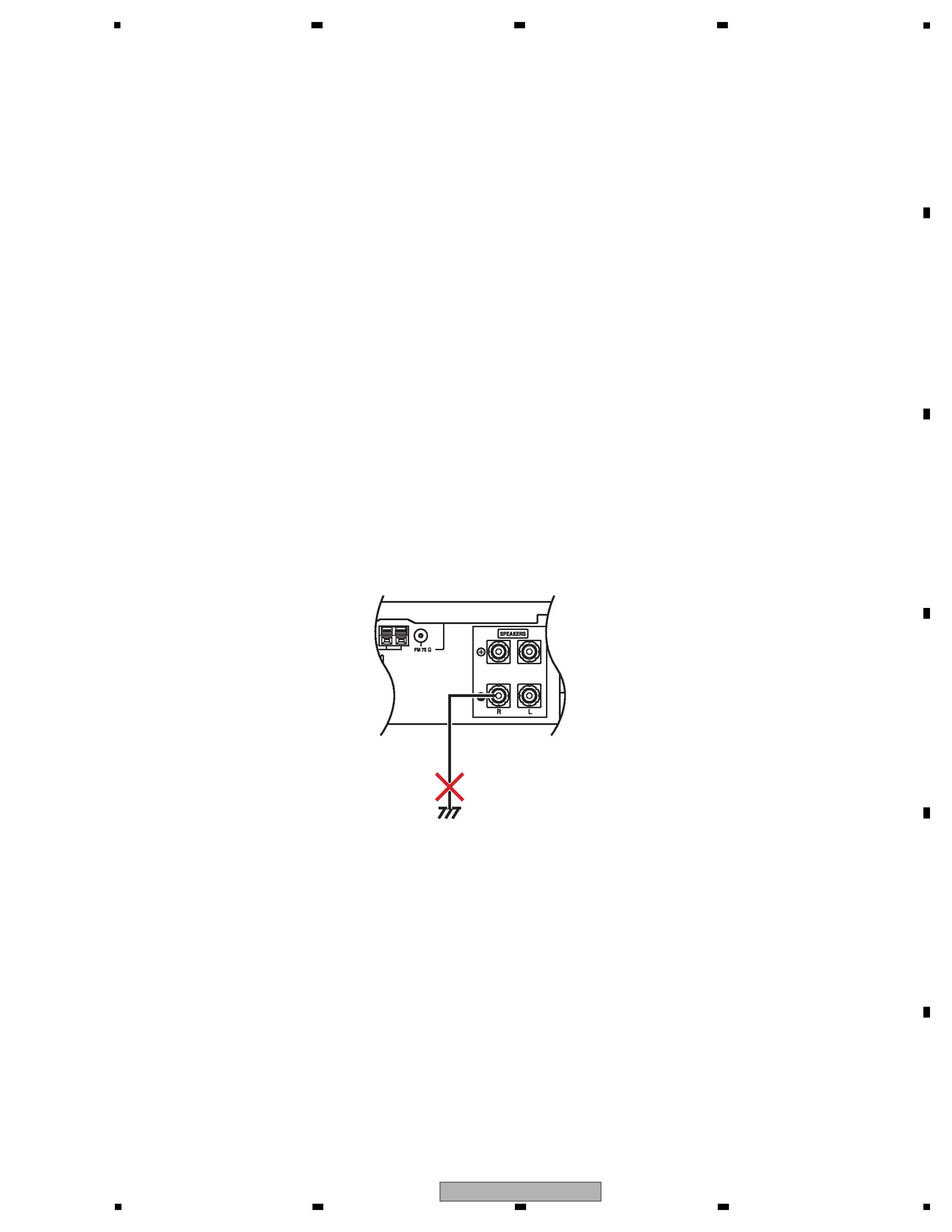
Negative Speaker Terminal
Ground (Chassis)
Do not short-circuit
As a signal to drive the BTL is output from the negative speaker terminal, DO NOT short-circuit between the
negative speaker terminal and ground, such as the chassis.