ORDER NO.
PIONEER CORPORATION 4-1, Meguro 1-chome, Meguro-ku, Tokyo 153-8654, Japan
PIONEER ELECTRONICS (USA) INC. P.O. Box 1760, Long Beach, CA 90801-1760, U.S.A.
PIONEER EUROPE NV Haven 1087, Keetberglaan 1, 9120 Melsele, Belgium
PIONEER ELECTRONICS ASIACENTRE PTE. LTD. 253 Alexandra Road, #04-01, Singapore 159936
PIONEER CORPORATION 2008
2008 Printed in Japan
KRP-M01
ARP3509
MEDIA RECEIVER
KRP-M01
THIS MANUAL IS APPLICABLE TO THE FOLLOWING MODEL(S) AND TYPE(S).
This service manual should be used together with the following manual(s).
Model
Type
Power Requirement
Remarks
KRP-M01
WYSIXK5
AC 220 V to 240 V
KRP-M01
WYSXJ5
AC 220 V to 240 V
Model No.
Order No.
Remarks
KRP-M01
ARP3508
EXPLODED VIEWS, BLOCK DIAGLAM, ADJUSTMENT, etc
For details, refer to "Important Check Points for good servicing".
T-ZZS-001 SEPT.
2
KRP-M01
1
2
3
4
A
B
C
D
E
F
1
2
3
4
[Important Check Points for Good Servicing]
In this manual, procedures that must be performed during repairs are marked with the below symbol.
Please be sure to confirm and follow these procedures.
1. Product safety
Please conform to product regulations (such as safety and radiation regulations), and maintain a safe servicing environment by
following the safety instructions described in this manual.
1 Use specified parts for repair.
Use genuine parts. Be sure to use important parts for safety.
2 Do not perform modifications without proper instructions.
Please follow the specified safety methods when modification(addition/change of parts) is required due to interferences such as
radio/TV interference and foreign noise.
3 Make sure the soldering of repaired locations is properly performed.
When you solder while repairing, please be sure that there are no cold solder and other debris.
Soldering should be finished with the proper quantity. (Refer to the example)
4 Make sure the screws are tightly fastened.
Please be sure that all screws are fastened, and that there are no loose screws.
5 Make sure each connectors are correctly inserted.
Please be sure that all connectors are inserted, and that there are no imperfect insertion.
6 Make sure the wiring cables are set to their original state.
Please replace the wiring and cables to the original state after repairs.
In addition, be sure that there are no pinched wires, etc.
7 Make sure screws and soldering scraps do not remain inside the product.
Please check that neither solder debris nor screws remain inside the product.
8 There should be no semi-broken wires, scratches, melting, etc.on the coating of the power cord.
Damaged power cords may lead to fire accidents, so please be sure that there are no damages.
If you find a damaged power cord, please exchange it with a suitable one.
9 There should be no spark traces or similar marks on the power plug.
When spark traces or similar marks are found on the power supply plug, please check the connection and advise on secure
connections and suitable usage. Please exchange the power cord if necessary.
a Safe environment should be secured during servicing.
When you perform repairs, please pay attention to static electricity, furniture, household articles, etc. in order to prevent injuries.
Please pay attention to your surroundings and repair safely.
2. Adjustments
To keep the original performance of the products, optimum adjustments and confirmation of characteristics within specification.
Adjustments should be performed in accordance with the procedures/instructions described in this manual.
4. Cleaning
For parts that require cleaning, such as optical pickups, tape deck heads, lenses and mirrors used in projection monitors, proper
cleaning should be performed to restore their performances.
3. Lubricants, Glues, and Replacement parts
Use grease and adhesives that are equal to the specified substance.
Make sure the proper amount is applied.
5. Shipping mode and Shipping screws
To protect products from damages or failures during transit, the shipping mode should be set or the shipping screws should be
installed before shipment. Please be sure to follow this method especially if it is specified in this manual.

3
KRP-M01
5
6
7
8
5
6
7
8
A
B
C
D
E
F
CONTENTS
10. SCHEMATIC DIAGRAM ...................................................................................................................................................... 4
10.1 OVERALL CONNECTION DIAGRAM........................................................................................................................... 4
10.2 MAIN BLOCK ASSY (1/33) [BOARD_IF_0 BLOCK] .................................................................................................... 6
10.3 MAIN BLOCK ASSY (2/33) [BOARD_IF_1 BLOCK] .................................................................................................... 8
10.4 MAIN BLOCK ASSY (3/33) [BOARD_IF_2 BLOCK] .................................................................................................. 10
10.5 MAIN BLOCK ASSY (4/33) [POWER_0 BLOCK] ....................................................................................................... 12
10.6 MAIN BLOCK ASSY (5/33) [POWER_1 BLOCK] ....................................................................................................... 14
10.7 MAIN BLOCK ASSY (6/33) [POWER_2 BLOCK] ....................................................................................................... 16
10.8 MAIN BLOCK ASSY (7/33) [POWER_3 BLOCK] ....................................................................................................... 18
10.9 MAIN BLOCK ASSY (8/33) [VDEC BLOCK] .............................................................................................................. 20
10.10 MAIN BLOCK ASSY (9/33) [ADC BLOCK] ............................................................................................................... 22
10.11 MAIN BLOCK ASSY (10/33) [HDMI_RX BLOCK] .................................................................................................... 24
10.12 MAIN BLOCK ASSY (11/33) [HDMI_SW BLOCK] ................................................................................................... 26
10.13 MAIN BLOCK ASSY (12/33) [AV_SW BLOCK] ........................................................................................................ 28
10.14 MAIN BLOCK ASSY (13/33) [RGB_SW BLOCK] ..................................................................................................... 30
10.15 MAIN BLOCK ASSY (14/33) [MSP BLOCK]............................................................................................................. 32
10.16 MAIN BLOCK ASSY (15/33) [DVB_S_TUNER BLOCK] .......................................................................................... 34
10.17 MAIN BLOCK ASSY (16/33) [DVB_T_TUNER BLOCK]........................................................................................... 36
10.18 MAIN BLOCK ASSY (17/33) [COFDM BLOCK] ....................................................................................................... 38
10.19 MAIN BLOCK ASSY (18/33) [TS_SELECT BLOCK]................................................................................................ 40
10.20 MAIN BLOCK ASSY (19/33) [CIMAX BLOCK] ......................................................................................................... 42
10.21 MAIN BLOCK ASSY (20/33) [CI_CARD_1 BLOCK]................................................................................................. 44
10.22 MAIN BLOCK ASSY (21/33) [VBI_SLICER BLOCK]................................................................................................ 46
10.23 MAIN BLOCK ASSY (22/33) [7404_0 BLOCK] ........................................................................................................ 48
10.24 MAIN BLOCK ASSY (23/33) [7404_1 BLOCK] ........................................................................................................ 50
10.25 MAIN BLOCK ASSY (24/33) [7404_DDR BLOCK]................................................................................................... 52
10.26 MAIN BLOCK ASSY (25/33) [7404_FLASH BLOCK] ............................................................................................... 54
10.27 MAIN BLOCK ASSY (26/33) [AV_IO BLOCK] .......................................................................................................... 56
10.28 MAIN BLOCK ASSY (27/33) [ARIA_0 BLOCK] ........................................................................................................ 58
10.29 MAIN BLOCK ASSY (28/33) [ARIA_1 BLOCK] ........................................................................................................ 60
10.30 MAIN BLOCK ASSY (29/33) [ARIA_DDR BLOCK] .................................................................................................. 62
10.31 MAIN BLOCK ASSY (30/33) [IF_UCOM BLOCK] .................................................................................................... 64
10.32 MAIN BLOCK ASSY (31/33) [EMMA2 BLOCK]........................................................................................................ 66
10.33 MAIN BLOCK ASSY (32/33) [EMMA2_MEM BLOCK] ............................................................................................. 68
10.34 MAIN BLOCK ASSY (33/33) [DP_TX BLOCK] ......................................................................................................... 70
10.35 FRONT_HDM_USB ASSY ....................................................................................................................................... 72
10.36 REAR IO ASSY (1/3) [BOARD_IF BLOCK] .............................................................................................................. 74
10.37 REAR IO ASSY (2/3) [IO_0 BLOCK] ........................................................................................................................ 76
10.38 REAR IO ASSY (3/3) [IO_1 BLOCK] ........................................................................................................................ 78
10.39 LED AND KEY ASSYS ............................................................................................................................................. 80
10.40 FRONT IO ASSY ...................................................................................................................................................... 82
10.41 CI CARD ASSY ........................................................................................................................................................ 84
10.42 VOLTAGES AND WAVEFORMS............................................................................................................................... 86
11. PCB CONNECTION DIAGRAM ........................................................................................................................................ 90
11.1 MAIN BLOCK AND FRONT_HDM_USB ASSYS ....................................................................................................... 90
11.2 REAR IO, LED, FRONT IO, CI CARD AND KEY ASSYS ........................................................................................... 94
12. PCB PARTS LIST .............................................................................................................................................................. 98
4
KRP-M01
1
2
3
4
A
B
C
D
E
F
1
2
3
4
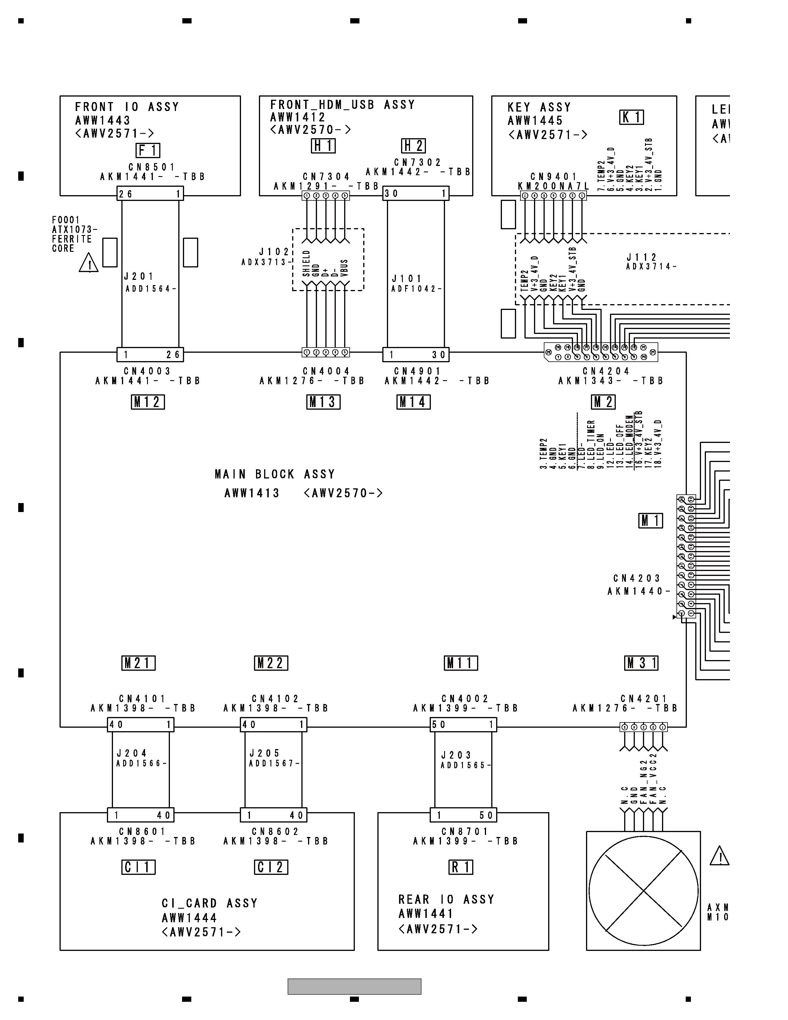
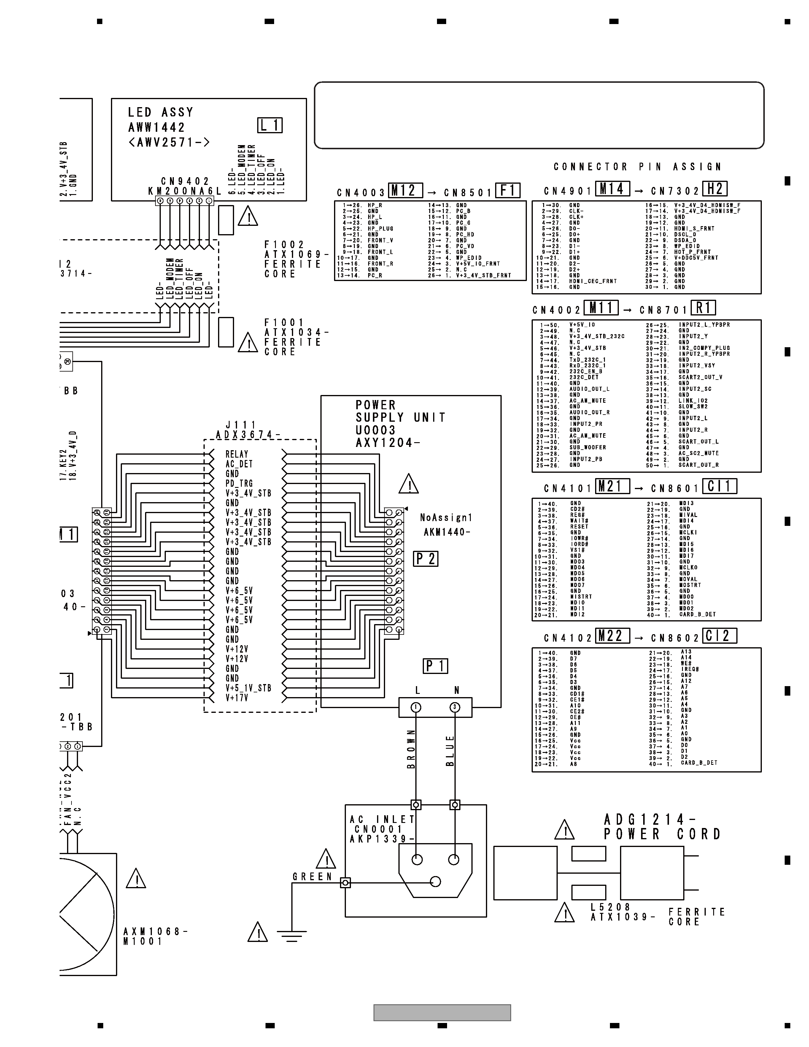
10. SCHEMATIC DIAGRAM
10.1 OVERALL CONNECTION DIAGRAM
5
KRP-M01
5
6
7
8
5
6
7
8
A
B
C
D
E
F
OVERALL DIAGRAM
k When ordering service parts, be sure to refer to "EXPLODED VIEWS and PARTS LIST" or
"PCB PARTS LIST".
k The
> mark found on some component parts indicates the importance of the safety factor
of the part. Therefore, when replacing, be sure to use parts of identical designation.
OVERALL DIAGRAM
KRP-M01
k When ordering service parts, be sure to refer to "EXPLODED VIEWS and PARTS LIST" or
"PCB PARTS LIST".
k The
> mark found on some component parts indicates the importance of the safety factor
of the part. Therefore, when replacing, be sure to use parts of identical designation.