ORDER NO.
PIONEER ELECTRONIC CORPORATION 4-1, Meguro 1-Chome, Meguro-ku, Tokyo 153-8654, Japan
PIONEER ELECTRONICS SERVICE, INC. P.O. Box 1760, Long Beach, CA 90801-1760, U.S.A.
PIONEER ELECTRONIC (EUROPE) N.V. Haven 1087, Keetberglaan 1, 9120 Melsele, Belgium
PIONEER ELECTRONICS ASIACENTRE PTE. LTD. 501 Orchard Road, #10-00 Wheelock Place, Singapore 238880
PIONEER ELECTRONIC CORPORATION 1998
RRV1980
DVD PLAYER
DV-606D
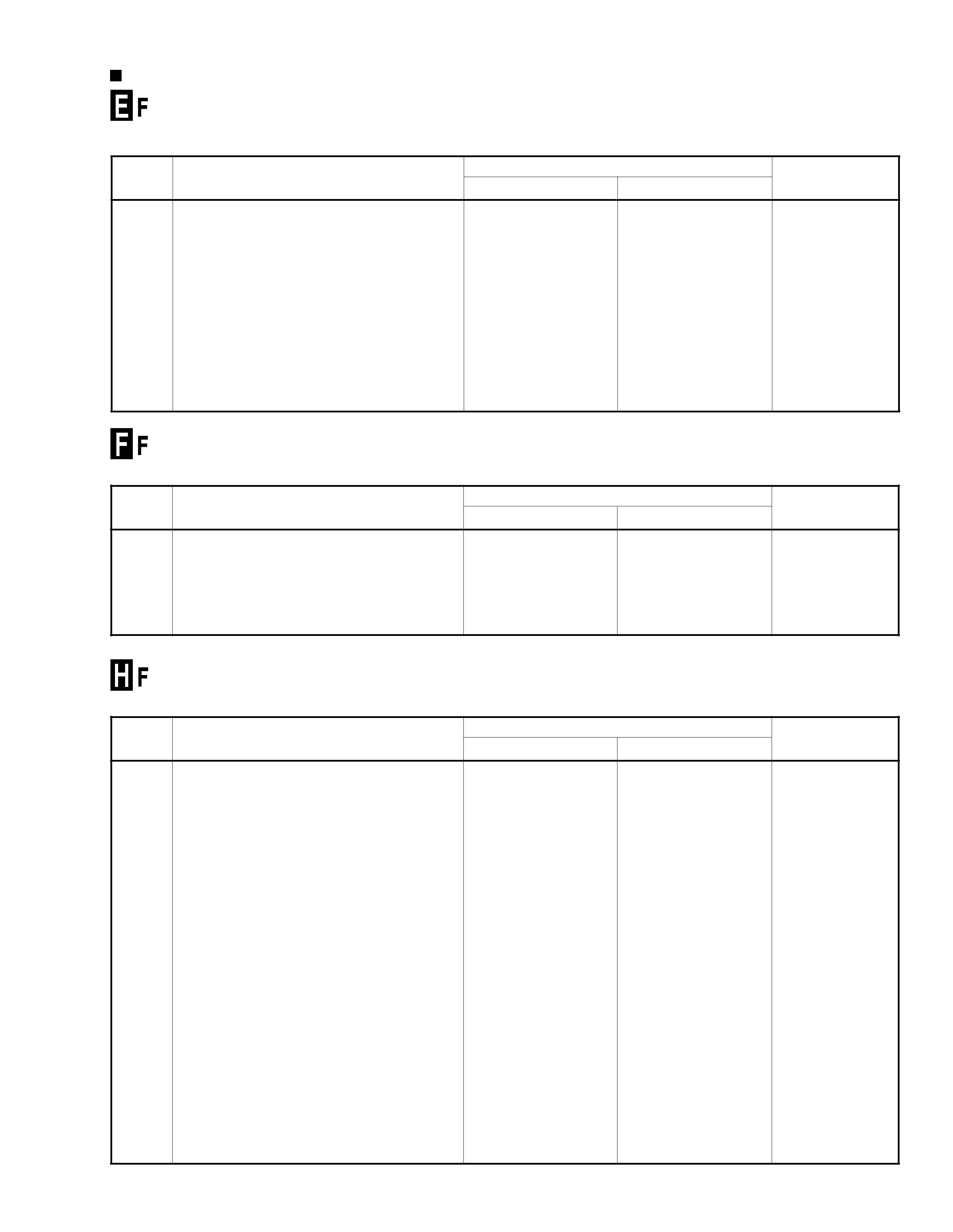
1. CONTRAST OF MISCELLANEOUS PARTS ........ 2
2. SCHEMATIC DIAGRAM ....................................... 8
3. PCB CONNECTION DIAGRAM .......................... 16
4. ADJUSTMENT .................................................... 18
5. IC INFORMATION .............................................. 19
CONTENTS
T ZZE JUNE 1998 Printed in Japan
÷ Refer to the service manual RRV1889 for DV-505/KU.
THIS MANUAL IS APPLICABLE TO THE FOLLOWING MODEL(S) AND TYPE(S).
Remarks
Power Requirement
Type
Model
DV-606D
L/TA
AC110V
3
Regional restriction
codes (region number)
DV-606D
2
1. CONTRAST OF MISCELLANEOUS PARTS
PCB ASSEMBLIES
FLKY Assy
VWM1789
VWM1793
P5 - 1
FLKB Assy
VWG1873
VWG1877
P5 - 2
NSP
PWSB Assy
VWG1879
VWG1939
P6 - 2
DVDM Assy
VWS1326
VWS1327
P6 - 3
AVJB Assy
VWV1572
VWV1606
PACKING
P3 - 1
Power Cord
ADG1126
ADG7002
P3 - 3
NSP
Warranty Card
ARY1044
Not used
P3 - 6
NSP
Dry Cell Battery (R6P, AA)
VEM-013
Not used
P3 - 6
NSP
Dry Cell Battery (R03, AAA)
Not used
VEM-022
P3 - 7
Operating Instructions (English)
VRB1183
Not used
Operating Instructions
Not used
VRC1073
No.1
(Trad. Chinese Language)
P3 - 9
Remote Control Unit (CU-DV008)
VXX2540
Not used
P3 -12
Battery Cover
VNK3703
Not used
Remote Control Unit (CU-DV019)
Not used
VXX2572
No.2
Battery Cover
Not used
VNK3684
No.3
Upper Cover
Not used
VNK3685
No.4
P3 -15
Packing Case
VHG1716
VHG1760
Remote Control Holder
Not used
VHC1044
No.5
EXTERIOR SECTION
P4 -18
65 Label
ORW1069
Not used
FRONT PANEL SECTION
P5 - 4
Front Panel
VNK4091
VNK4290
P5 - 5
FL Lens
VNK4149
VEC1985
Display Button
Not used
VNK3649
No.6
Button
Not used
VNK4287
No.7
NSP
DTS Label
Not used
VRW1732
No.8
Earth Plate
Not used
VNE2085
No.9
Ref.
No.
Remarks
DV-505/KU
DV-606D/L/TA
Part No.
Mark
Symbol and Description
7 CONTRAST TABLE
DV-606D/L/TA and DV-505/KU are constructed the same except for the following:
NOTES :
÷ Parts marked by " NSP " are generally unavailable because they are not in our Master Spare Parts List.
÷ The
mark found on some component parts indicates the importance of the safety factor of the part.
Therefore, when replacing, be sure to use parts of identical designation.
÷ Reference Nos. indicate the pages and Nos. in the service manual for the base model.
÷ When ordering resistors, first convert resistance values into code form as shown in the following examples.
Ex. 1
When there are 2 effective digits (any digit apart from 0), such as 560 ohm and 47k ohm (tolerance is shown by
J = 5%, and K = 10%).
560
= 56 × 101= 561 ................................................... RD1/4PU 5 6 1 J
47k
= 47 × 10 3 = 473 .................................................. RD1/4PU 4 7 3 J
0.5
= R50 ...................................................................... RN2H Â 5 0 K
1
= 1R0 ......................................................................... RS1P 1 Â 0 K
Ex. 2
When there are 3 effective digits (such as in high precision metal film resistors).
5.62k
= 562 × 10 1 = 5621 ........................................... RN1/4PC 5 6 2 1 F
DV-606D
3
BOTTOM VIEW SECTION
P6 -19
Flexible Cable (14P)
VDA1646
VDA1684
No.10
P6 -21
Rear Panel
VNA1903
VNA2009
P6 -22
Housing Assy (4P)
VKP2157
VKP2190
P6 -26
Fuse Caution Label
VRW1693
Not used
Flexible Cable (7P)
Not used
VDA1685
No.11
(AVJB CN102 DVDM CN804)
Ref.
No.
Remarks
DV-505/KU
DV-606D/L/TA
Part No.
Mark
Symbol and Description
Note:
÷ The numbers in the remarks column correspond to the numbers on " EXPLODED VIEWS ".
÷ For PCB ASSEMBLIES, refer to " CONTRAST OF PCB ASSEMBLIES " , " PCB PARTS LIST " , " 2. SCHEMATIC DIAGRAM "
and " 3. PCB CONNECTION DIAGRAM ".
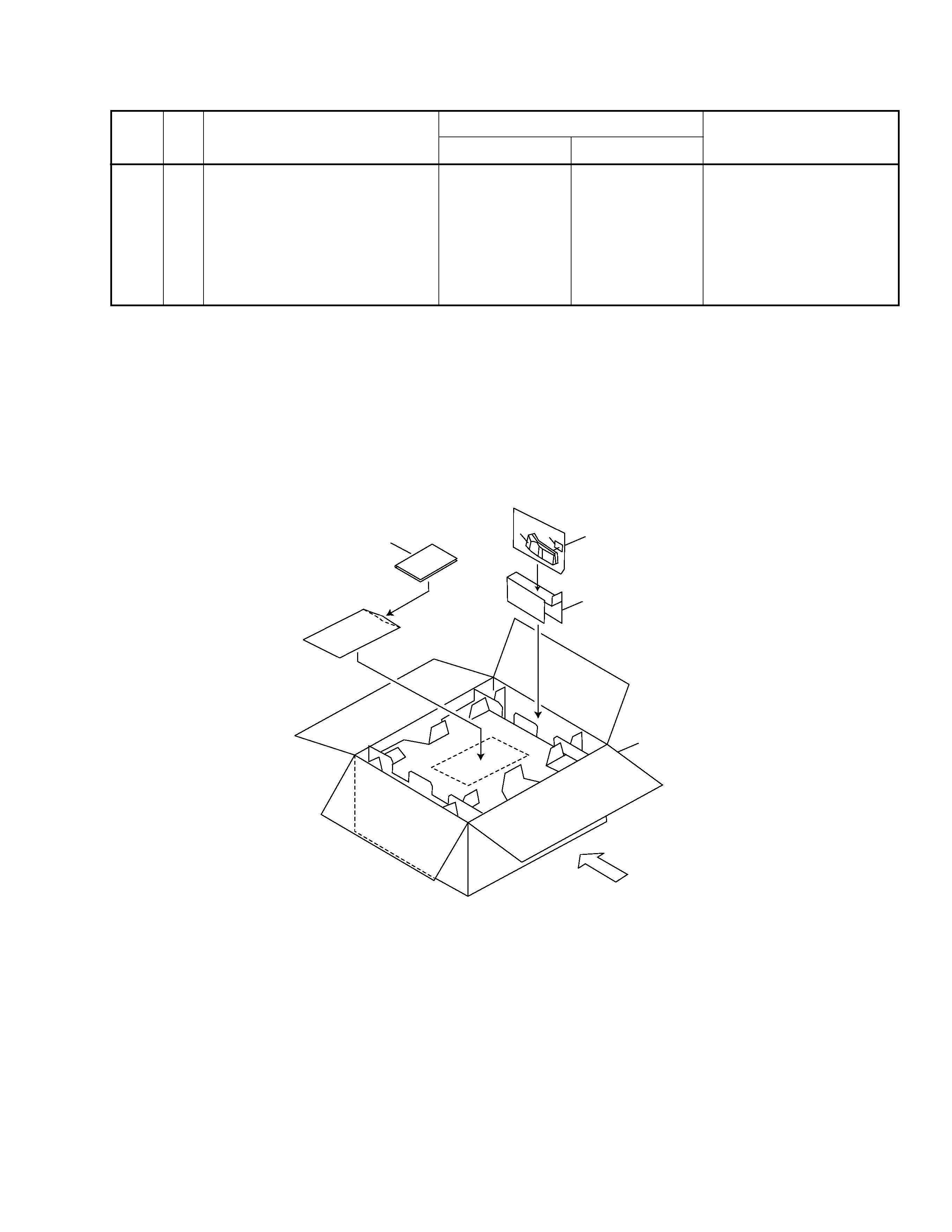
2
5
FRONT
PACKING CASE
1
3
4
÷ PACKING SECTION
7 EXPLODED VIEWS
DV-606D
4
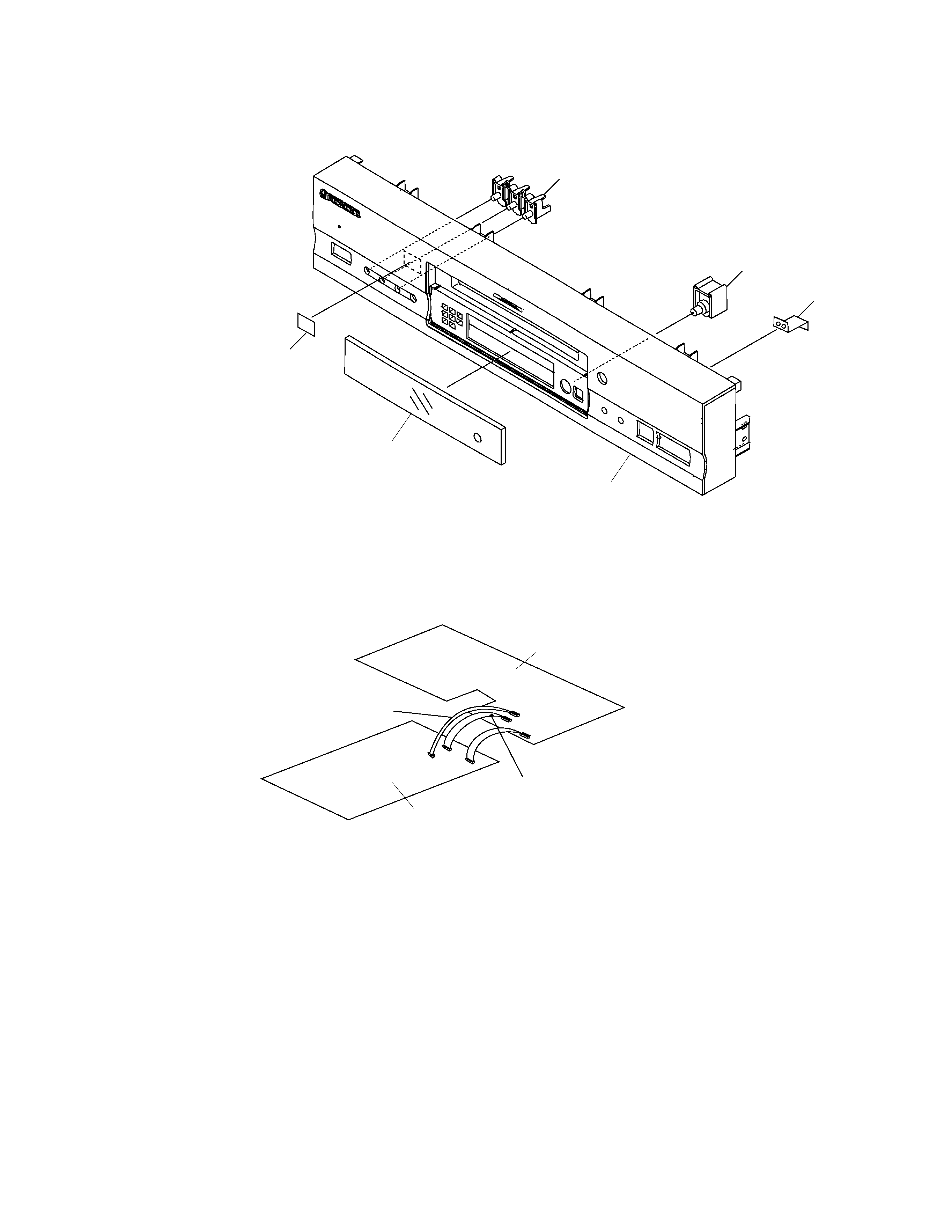
7
FL Lens
6
8
FRONT PANEL
9
÷ FRONT PANEL SECTION
÷ BOTTOM VIEW SECTION
CN804
CN803
CN802
CN104
CN101
CN102
DVDM ASSY
AVJB ASSY
10
(Set the marking side to the AVJB ASSY CN101.)
11
DV-606D
5
CONTRAST OF PCB ASSEMBLIES
VWG1877 and VWG1873 are constructed the same except for the following :
FLKB ASSY
VWG1939 and VWG1879 are constructed the same except for the following :
PWSB ASSY
k
r
a
Mn
o
i
t
p
i
r
c
s
e
D
d
n
a
l
o
b
m
y
S
.
o
N
t
r
a
P
s
k
r
a
m
e
R
9
7
8
1
G
W
V9
3
9
1
G
W
V
2
0
2
RJ
1
8
1
S
0
1
/
1
S
RJ
1
3
3
S
0
1
/
1
S
R
3
1
2
Rd
e
s
u
t
o
NJ
2
3
4
S
0
1
/
1
S
R
4
1
2
Rd
e
s
u
t
o
NJ
2
2
6
S
0
1
/
1
S
R
5
1
2
Rd
e
s
u
t
o
NJ
3
0
1
S
0
1
/
1
S
R
5
0
2
S
-
3
0
2
Sd
e
s
u
t
o
N0
3
0
1
G
S
R
VWS1327 and VWS1326 are constructed the same except for the following :
DVDM ASSY
k
r
a
Mn
o
i
t
p
i
r
c
s
e
D
d
n
a
l
o
b
m
y
S
.
o
N
t
r
a
P
s
k
r
a
m
e
R
6
2
3
1
S
W
V7
2
3
1
S
W
V
2
0
6
C
Id
e
s
u
t
o
NC
6
2
0
K
D
P
3
0
0
6
C
I5
6
5
1
W
Y
V1
7
5
1
W
Y
V
1
2
9
9
F
,
1
4
1
9
Fd
e
s
u
t
o
N6
9
0
1
F
T
V
1
3
9
9
L
,
0
3
9
9
L
,
3
4
1
9
Ld
e
s
u
t
o
N1
1
0
1
L
T
Q
7
0
6
C
,
6
0
6
Cd
e
s
u
t
o
N6
1
Z
4
0
1
F
Y
R
S
K
C
1
Rd
e
s
u
t
o
NJ
3
2
2
S
6
1
/
1
S
R
2
RJ
3
0
1
S
6
1
/
1
S
RJ
3
3
3
S
6
1
/
1
S
R
5
3
9
R
,
1
2
9
R
,
0
2
9
R
,
1
4
1
RJ
0
R
0
S
0
1
/
1
S
Rd
e
s
u
t
o
N
3
4
1
RJ
0
R
0
S
6
1
/
1
S
Rd
e
s
u
t
o
N
1
4
6
Rd
e
s
u
t
o
NJ
0
R
0
S
6
1
/
1
S
R
2
4
6
Rd
e
s
u
t
o
NJ
3
0
1
S
6
1
/
1
S
R
0
3
8
Rd
e
s
u
t
o
NJ
1
0
2
S
6
1
/
1
S
R
5
2
9
R
,
6
6
8
R
-
4
6
8
Rd
e
s
u
t
o
NJ
1
0
1
S
6
1
/
1
S
R
2
3
9
R
,
6
2
9
R
,
4
2
9
R
,
3
2
9
RJ
0
2
2
S
6
1
/
1
S
RJ
1
0
1
S
6
1
/
1
S
R
2
6
9
R
,
1
3
9
R
,
0
3
9
RJ
0
2
2
S
6
1
/
1
S
Rd
e
s
u
t
o
N
7
3
9
RJ
1
3
3
S
6
1
/
1
S
RJ
1
7
2
S
6
1
/
1
S
R
8
3
9
RJ
0
2
2
S
6
1
/
1
S
RJ
1
6
5
S
6
1
/
1
S
R
0
4
9
RJ
0
2
2
S
6
1
/
1
S
RJ
1
3
3
S
6
1
/
1
S
R
4
0
8
N
Cd
e
s
u
t
o
N1
1
4
1
N
K
V
k
r
a
Mn
o
i
t
p
i
r
c
s
e
D
d
n
a
l
o
b
m
y
S
.
o
N
t
r
a
P
s
k
r
a
m
e
R
3
7
8
1
G
W
V7
7
8
1
G
W
V
8
0
1
Q
-
6
0
1
Q
,
4
0
1
Q
,
1
0
1
Qd
e
s
u
t
o
NK
E
4
2
1
C
T
D
P
8
0
1
D
-
1
0
1
Dd
e
s
u
t
o
NH
1
5
C
8
1
1
4
P
L
S
8
0
1
R
-
1
0
1
Rd
e
s
u
t
o
NJ
1
3
3
S
0
1
/
1
S
R
4
2
1
RJ
0
R
0
S
0
1
/
1
S
Rd
e
s
u
t
o
N
6
0
6
R
,
6
2
1
Rd
e
s
u
t
o
NJ
0
R
0
S
0
1
/
1
S
R
7
2
1
RJ
0
R
0
S
0
1
/
1
S
RJ
3
7
2
S
0
1
/
1
S
R
8
2
1
RJ
2
2
6
S
0
1
/
1
S
RJ
3
2
1
S
0
1
/
1
S
R
7
3
1
Rd
e
s
u
t
o
NJ
3
8
6
S
0
1
/
1
S
R
8
3
1
RJ
3
6
3
S
0
1
/
1
S
RJ
2
7
4
S
0
1
/
1
S
R
1
0
1
Sd
e
s
u
t
o
N0
3
0
1
G
S
R