
Model
Service Manual
CD Mechanism Module
DEH-P90DAB/EW, ES
CRT2556
CXK5301
PIONEER CORPORATION
4-1, Meguro 1-Chome, Meguro-ku, Tokyo 153-8654, Japan
PIONEER ELECTRONICS SERVICE INC.
P.O.Box 1760, Long Beach, CA 90801-1760 U.S.A.
PIONEER EUROPE NV
Haven 1087 Keetberglaan 1, 9120 Melsele, Belgium
PIONEER ELECTRONICS ASIACENTRE PTE.LTD. 253 Alexandra Road, #04-01, Singapore 159936
C PIONEER CORPORATION 2000
K-ZZA. NOV. 2000 Printed in Japan
ORDER NO.
CRT2503
CD MECHANISM MODULE
CX-961
Service
Manual
- This service manual describes the operation of the CD mechanism module incorporated in models
listed in the table below.
- When performing repairs use this manual together with the specific manual for model under repair.
CONTENTS
1. CIRCUIT DESCRIPTIONS ...........................................2
2. MECHANISM DESCRIPTIONS.................................15
3. DISASSEMBLY .........................................................17
2
CX-961
1. CIRCUIT DESCRIPTIONS
This unit is roughly divided into the preamplifier stage, servo unit, power supply unit and loading control unit. This
LSI (large scale integrated circuit) implements eight automatic adjustments according to the combination of the
preamplifier stage and servo unit used.
Besides, because this system conforms to the single power supply (+5 V) specifications, the reference voltages of
servo systems (preamplifier, servo DSP and pickup) are all Vref (2. 1 V).
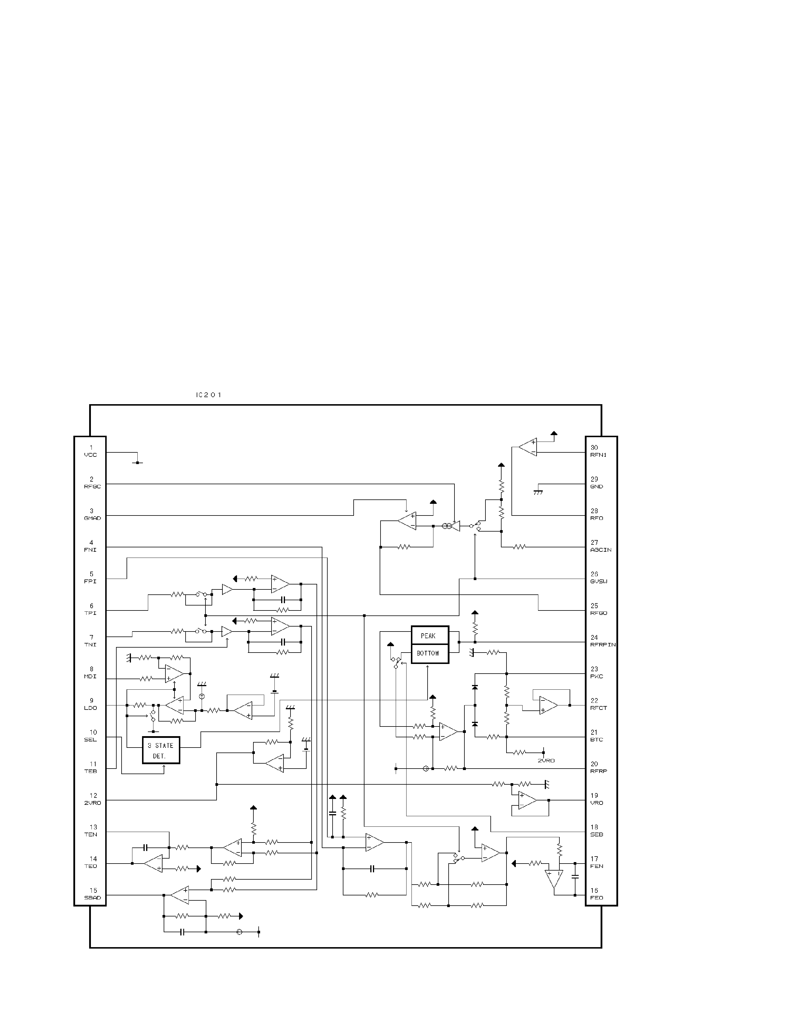
1.1 Preamplifier (TA2150FN; IC201)
The preamplifier processes output signal from the
pickup, then generates signals to the servo unit,
demodulator unit and control unit at the next stage, and
controls power for the pickup's laser diode. The signal
from the pickup is I-V converted by the preamplifier
built into the pickup's photodetector, then added by the
RF amplifier to obtain such signals as RF, FE and TE.
Reference voltage Vref (2.1 V) is output from pin 19 of
this IC and 2 Vref (4.2 V) is supplied as the reference
voltage which determines the D range of the servo DSP
A/D input.
Fig.1:TA2150FN CIRCUIT
3
CX-961
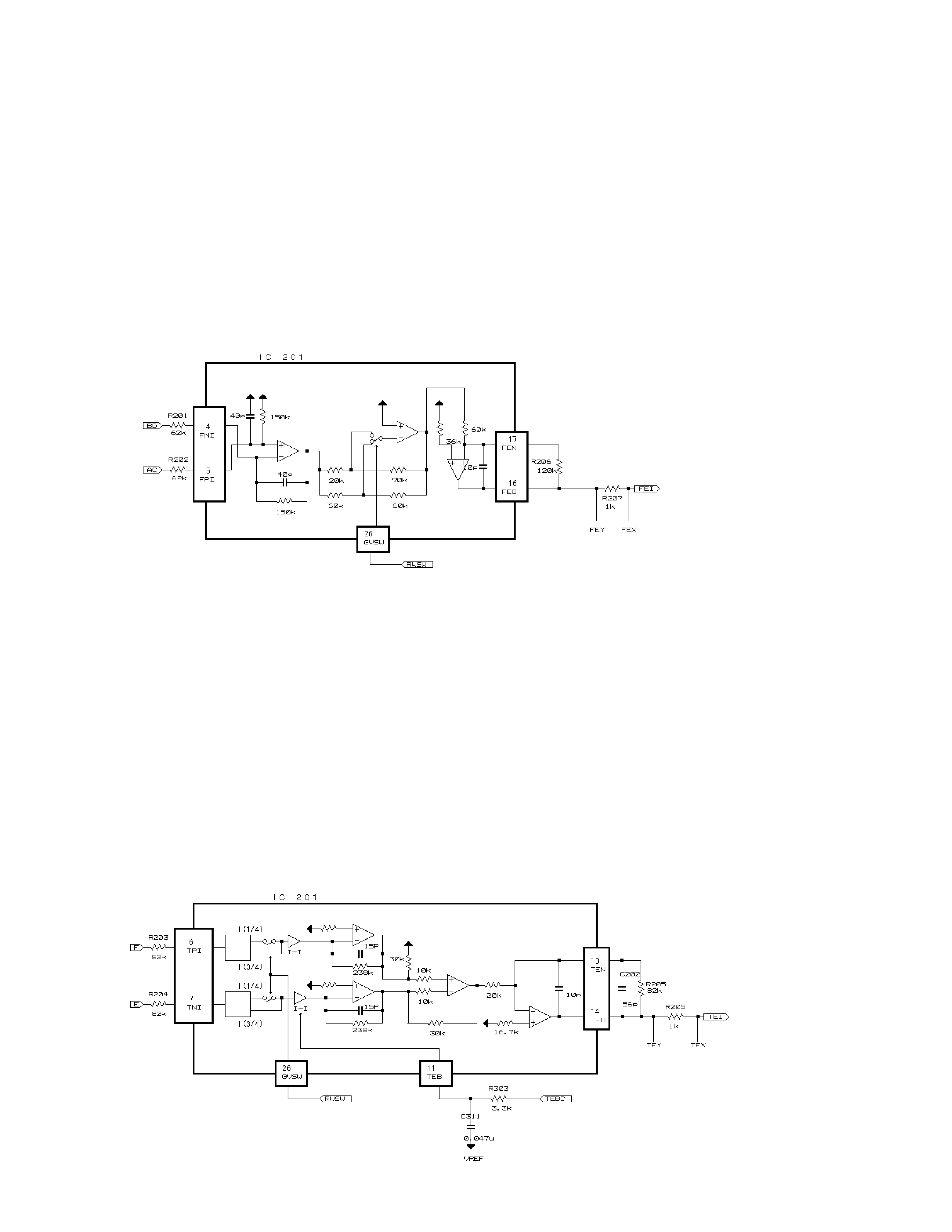
2) Tracking error amplifier unit
This tracking error amplifier unit outputs photodetector
output E or F from pin 14 of IC201 (TA2150FN)via an
amplifier and an error amplifier assuming (E - F) as a TE
signal. The low frequency component of voltage TE is
expressed as
TE = (E - F)
× 300 k / 100 k × 155 k / 328 k × 82 k / 20 k =
5.8 times.
A TE waveform of approximately 1.51 Vpp is obtained
in the TE output on the basis of Vref. The cutoff
frequency is 44.5 kHz or 29.4 kHz.
1) Focus error amplifier unit
This focus error amplifier outputs photodetector output
(A + C) or (B + D) from pin 16 of IC201 (TA2150FN) via a
differential amplifier and an error amplifier assuming
(A + C - B -C) as an FE signal. The low frequency
component of voltage FE is expressed as
FE = (A + C - B - D)
× (150 k / 62 k) × (60 k / 60 k) × (12 k /
60 k) = 4.84 times.
An S curve of approximately 1.45 Vpp is obtained in the
FE output on the basis of Vref. The cutoff frequency is
26 kHz or 133 kHz.
Fig.2:FE CIRCUIT
Fig.3:TE CIRCUIT
4
CX-961
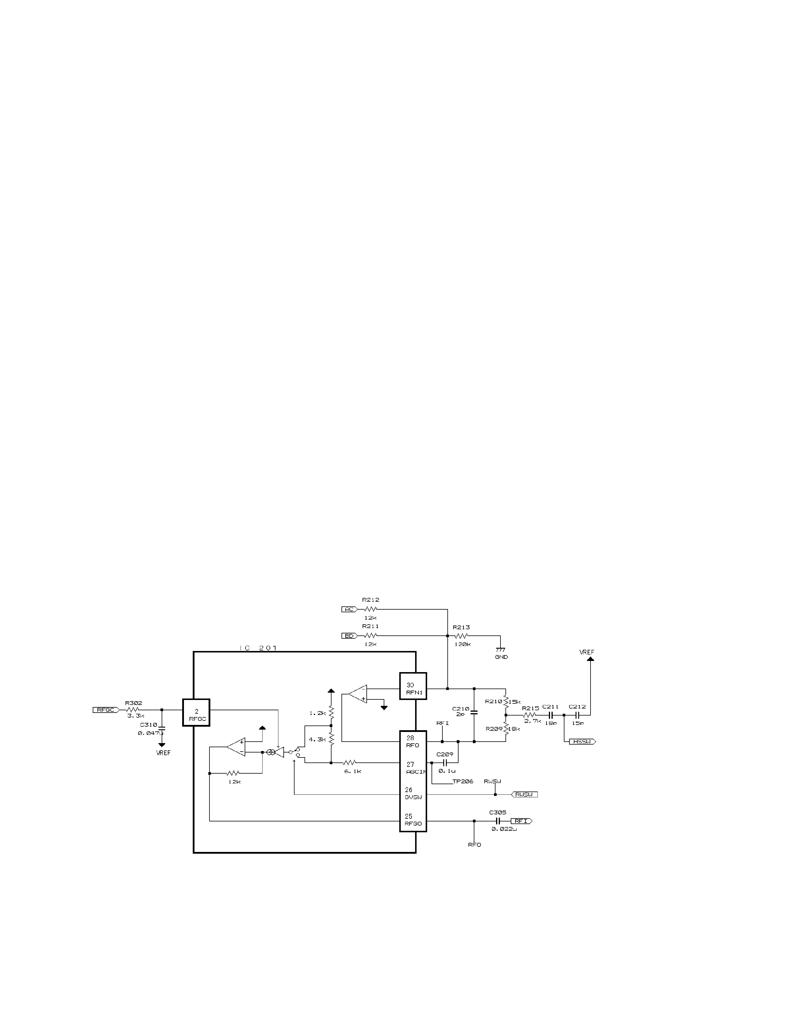
3) RF amplifier unit
The head amplifier LSI, TA2150FN, adds, amplifies and
equalizes photodetector output (A+C) and (B+D), then
outputs RF signal to the RFI pin. (This signal enables
checking eye patterns.) Low frequency element
contained in RFI voltage is formulated as follows:
RFI = (A + B + C + D)
× 5.43.
RFI is used for RF Offset Control circuit. RFI signal
output from Pin 28 is AC-coupled externally, and then
re-input to Pin 27 and amplified by the RFAG amplifier
to obtain RFO signal.
As described later, TA2150FN has a built-in RFAGC
function that controls the RFAGC amplifier gain so that
RFO output stays within 1.2 ± 0.3V p.p. range.
This RFO signal is used for EFM and RFAGC control
circuit and for generating RFRP and RFCT signals for
track counting.
Besides, the frequency characteristics of an RF
equalizer are switched at double-speed reproduction.
(Switching using the HSSW terminal)
Further, with RWSW the gain at the RF amplifier stage
is raised by 13db, compared with that in normal
operation, when the gain lowers because of stains on
the lens or while playing a CDRW.
Fig.4:RF CIRCUIT
5
CX-961
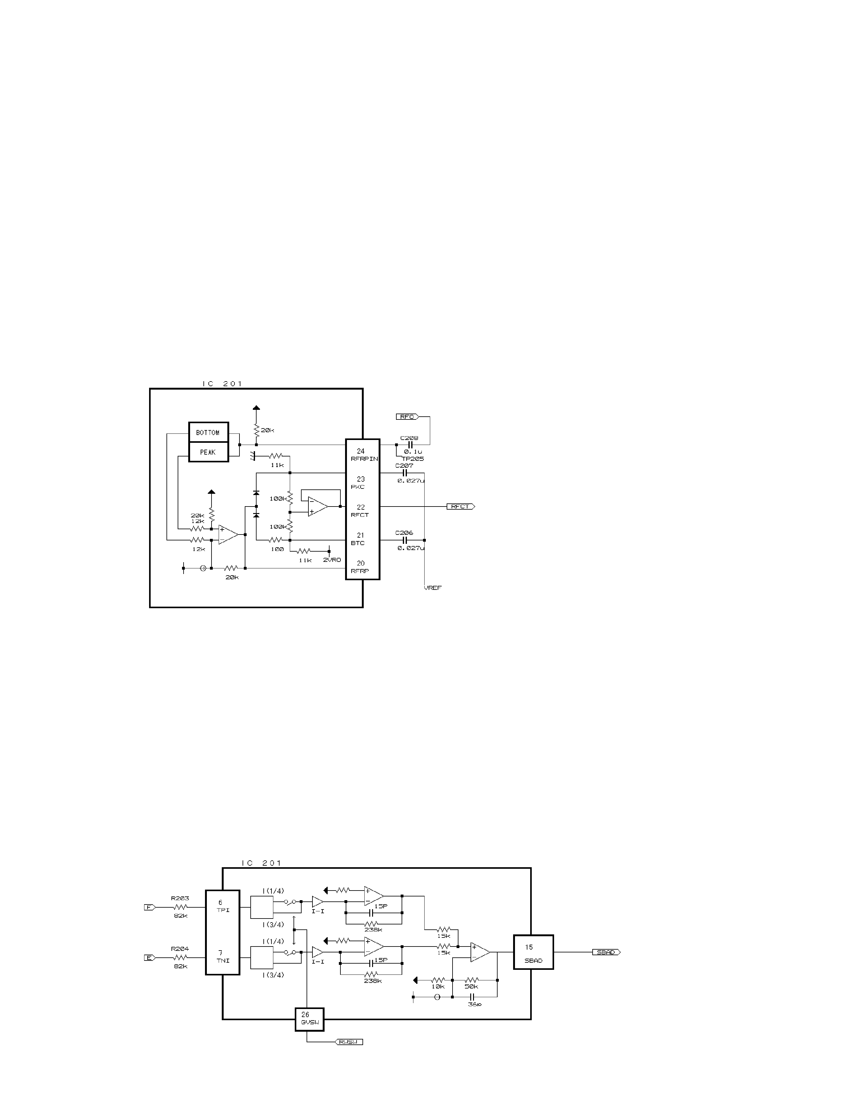
4) RFRP and RFCT signal circuit unit
The RFCT signal which is the difference signal between
the peak and bottom levels of the RF signal is
generated through head amplifier (IC201). RFRP and
RFCT can be monitored at TP203 (pin 20 of IC201
TA2150FN) and TP204 (pin 22 of IC201) respectively.
The TE, RFRP and RFCT signals are compared by a
hysteresis comparator inside IC301 (TC9495FP)
respectively and generate track information (TEZC
signal or RFZC signal). Based on this signal, the
traveling speed information about a lens disk is
generated and the number of tracks is counted.
5) SBAD signal circuit unit
This SBAD signal circuit unit outputs photodetector
output E and F from IC201 (pin 15 of TA2150FN) via an
addition amplifier assuming (E + F) as an SBAD signal.
This SBAD signal is used as the internal decision
conditions of focus ON/OFF with a focus error signal.
Further, the SBAD signal is also used for detecting
defects when disk scratches are passed.
Fig.5:RFRP AND RFCT SIGNAL CIRCUIT
Fig.6:SBAD SIGNAL CIRCUIT