ORDER NO.
PIONEER ELECTRONIC CORPORATION 4-1, Meguro 1-Chome, Meguro-ku, Tokyo 153-8654, Japan
PIONEER ELECTRONICS SERVICE, INC. P.O. Box 1760, Long Beach, CA 90801-1760, U.S.A.
PIONEER ELECTRONIC (EUROPE) N.V. Haven 1087, Keetberglaan 1, 9120 Melsele, Belgium
PIONEER ELECTRONICS ASIACENTRE PTE. LTD. 501 Orchard Road, #10-00 Wheelock Place, Singapore 238880
PIONEER ELECTRONIC CORPORATION 1998
STEREO CASSETTE DECK
RRV2039
TDZE OCT. 1998 Printed in Japan
CT-S550S
1. CONTRAST OF MISCELLANEOUS PARTS ..... 2
2. SCHEMATIC DIAGRAM ..................................... 4
3. PCB CONNECTION DIAGRAM ......................... 5
CONTENTS
¶ Refer to the service manual RRV1498 for CT-S550S/HYXJ.
Remarks
Type
Model
CT-S550S
Power Requirement
HYXJ7
AC220230V
HYXJ/GR7
AC220230V
THIS MANUAL IS APPLICABLE TO THE FOLLOWING MODEL(S) AND TYPE(S).
CT-S550S
2
NSP
MOTHER UNIT
RWM1908
RWM2053
RWM2053
P244
MAIN UNIT
RWZ3857
RWZ4318
RWZ4318
P245
DOLBY S UNIT
RWX1120
RWX1120
RWX1120
P223
FL UNIT
RWZ3859
RWZ4319
RWZ4319
P234
OPSW UNIT
RWZ3861
RWZ4320
RWZ4320
1
P252
NSP
POCM UNIT
RWZ3867
RWZ4321
RWZ4321
2
P237
NSP
TRN 2 UNIT
RWZ3865
RWZ4322
RWZ4322
3
POWER SW UNIT
Not used
RWX1150
RWX1150
4 No. 1, 5
P21
Name Plate
PAM1608
PAM1776
PAM1776
P22
Front Panel
RAH2719
RAH2872
RAH2872
P214
Power Cap
RAC1998
Not used
Not used
P216
Panel Stay
REA1196
REA1289
REA1289
P241
NSP
Main Chassis
RNB1113
RNB1132
RNB1132
P236
NSP
TRN 1 PCB
RNZ3004
RNZ3316
RNZ3316
P246
Rear Panel
RNA2034
RNA2214
RNA2214
P248
AC Power Cord
PDG1043
PDG1058
PDG1058
P266
Packing Case
RHG1737
RHG1880
RHG1880
P270
Operating Instructions
RRD1185
RRD1204
Not used
(French/Italian/Dutch/Swedish/
Spanish/Portuguese)
P271
Operating Instructions
RRE1136
RRE1168
RRE1168
(English/German)
P273
NSP
Warranty Card
ARY7009
ARY7022
ARY7022
NSP
PCB Holder
Not used
AEC703
AEC703
4 No. 2
Power Button
Not used
RAC2218
RAC2218
4 No. 3
1. CONTRAST OF MISCELLANEOUS PARTS
CONTRAST TABLE
Part No.
Remarks
CT-S550S
CT-S550S
CT-S550S
HYXJ
HYXJ7
HYXJ/GR7
CT-S550S/HYXJ7, HYXJ/GR7 and CT-S550S/HYXJ are constructed the same except for the following:
*1: Although RWZ4320 and RWZ3861 are different in part number, they have same service parts.
*2: Although RWZ4321 and RWZ3867 are different in part number, they have same service parts.
*3: Although RWZ4322 and RWZ3865 are different in part number, they have same service parts.
*4: The numbers in the remarks column correspond to the numbers on the " EXPLODED VIEWS ".
*5: Refer to " PCB PARTS LIST", " 2. SCHEMATIC DIAGRAM" and " 3. PCB CONNECTION DIAGRAM".
Ref.
No.
Mark
Symbol and Description
NOTES :
÷ Parts marked by " NSP " are generally unavailable because they are not in our Master Spare Parts List.
÷ The
mark found on some component parts indicates the importance of the safety factor of the part.
Therefore, when replacing, be sure to use parts of identical designation.
÷ When ordering resistors, first convert resistance values into code form as shown in the following examples.
Ex. 1
When there are 2 effective digits (any digit apart from 0), such as 560 ohm and 47k ohm (tolerance is shown by
J = 5%, and K = 10%).
560
= 56 × 101= 561 ................................................... RD1/4PU 5 6 1 J
47k
= 47 × 10 3 = 473 .................................................. RD1/4PU 4 7 3 J
0.5
= R50 ...................................................................... RN2H Â 5 0 K
1
= 1R0 ......................................................................... RS1P 1 Â 0 K
Ex. 2
When there are 3 effective digits (such as in high precision metal film resistors).
5.62k
= 562 × 10 1 = 5621 ........................................... RN1/4PC 5 6 2 1 F
÷ Reference Nos. indicate the pages and Nos. in the service manual for the base model.
CT-S550S
3
1
2
3
BBZ30P060FCC
Chassis
C101, C102
CQPA271J2A
CQHA271J2A
C119, C120
CKCYB101K50
CCCCH101J50
C153, C154, C179, C411, C501
CEAS470M16
CEAT470M16
C155, C156, C193, C194, C351, C803,
CEAS100M50
CEAT100M50
C1005, C1006
C175, C176, C181, C187C189, C201,
CEAS4R7M50
CEAT4R7M50
C202, C303, C304, C1014, C1023
C180, C184, C185, C190, C207, C208,
CEAS101M10
CEAT101M10
C307, C308, C603, C604
C183, C263, C264, C301, C302, C352,
CEAS1R0M50
CEAT1R0M50
C752
C203, C204, C255, C256, C464, C1107,
CEASR10M50
CEATR10M50
C1108
C253, C254, C259, C260, C305, C306,
CEAS330M16
CEAT330M16
C417, C465
C309, C310
CQPA181J2A
CQHA181J2A
C412, C415
CQMZA332J50
CQMA332J50
C414
CQMZA682J50
CQMA682J50
C551
CEASR47M50
CEATR47M50
C1003, C1004
CEAS222M16
CEAT222M16
C1009, C1010
CEAS221M25
CEAT221M25
C1015
CEAS332M25
CEAT332M25
C1016, C1019, C1021
CEAS101M50
CEAT101M50
C1022
CEAS102M6R3
CEAT102M6R3
C1024
CEAS220M16
CEAT220M25
C1111C1114
CQMZA562J50
CQMA562J50
VR101, VR102, VR451, VR452 (47 k
)
RCP1047
VCP1160
VR301, VR302, VR1101, VR1102 (22 k
)
RCP1046
VCP1158
NSP
J2001
XDF537
Not used
J2001
Not used
DB020NT0
EXPLODED VIEWS
CONTRAST OF PCB ASSEMBLIES
MAIN UNIT
RWZ4318 and RWZ3857 are constructed the same except for the following:
Mark
Remarks
Symbol and Description
Part No.
RWZ3857
RWZ4318
CT-S550S
4
TRN
2
UNIT
(RWZ4322)
TRN
1
PCB
(RNZ3316)
POWER SW UNIT
(RWX1150)
POWER TRANSFORMER
RTT1309
AC POWER CORD
PDG1058
10000pF/AC250V
3.2 MAIN, MECHANISM, FL, OPSW, POCM, TRN2 UNIT AND TRN1 PCB
SCH-2
SCH-2
PDF1004
LIVE
NEUTRAL
PDF1035
FL UNIT
RWZ4319 and RWZ3859 are constructed the same except for the following:
S1507 (POWER)
RSG1030
Not used
Mark
Remarks
Symbol and Description
Part No.
RWZ3859
RWZ4319
PCB PARTS LIST
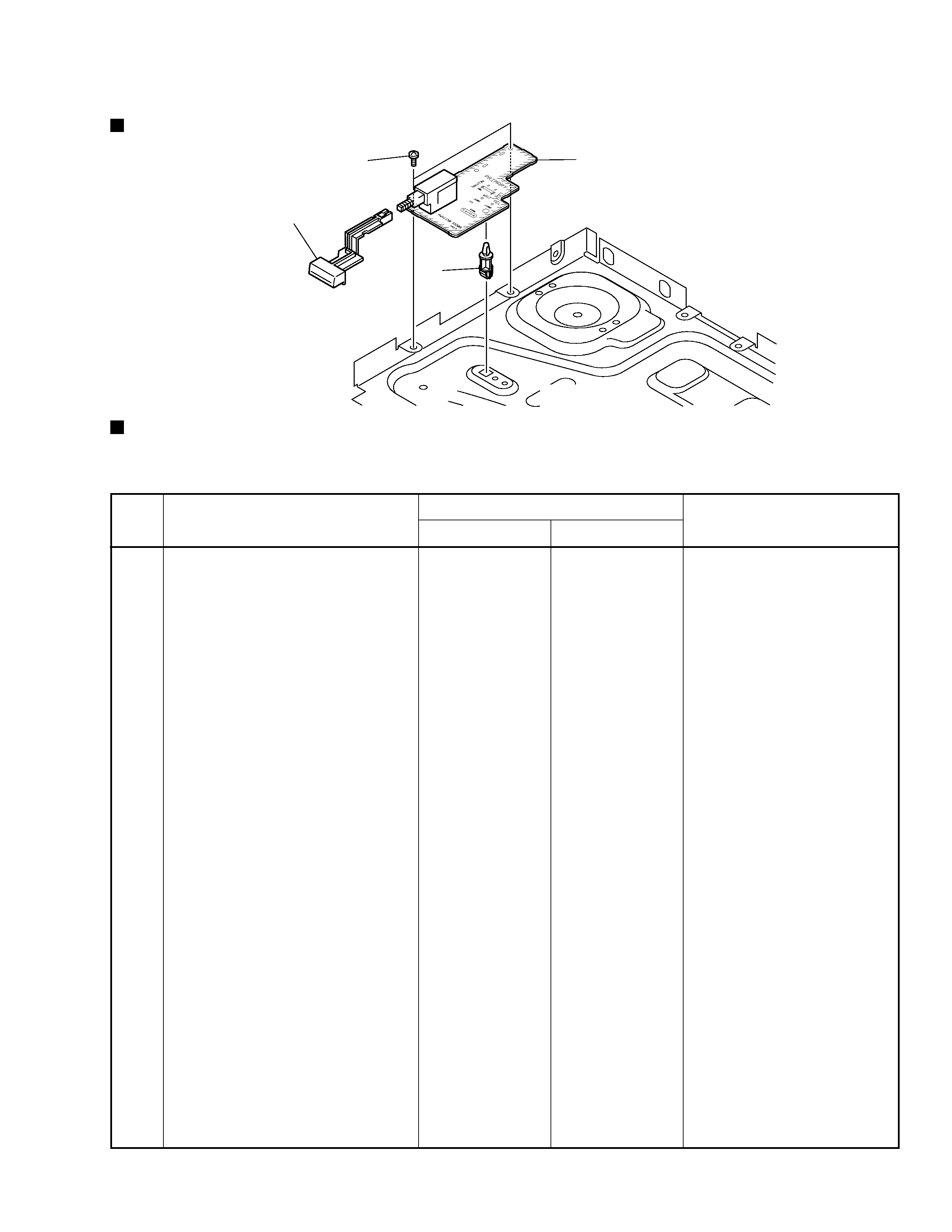
POWER SW UNIT
SWITCHES AND RELAYS
S1201
RSA1001
CAPACITOR
C1201 (10000 pF/AC250V)
ACG7020
OTHERS
1201
TERMINAL
RKC061
PCB BINDER
VEF1040
Mark No.
Description
Part No.
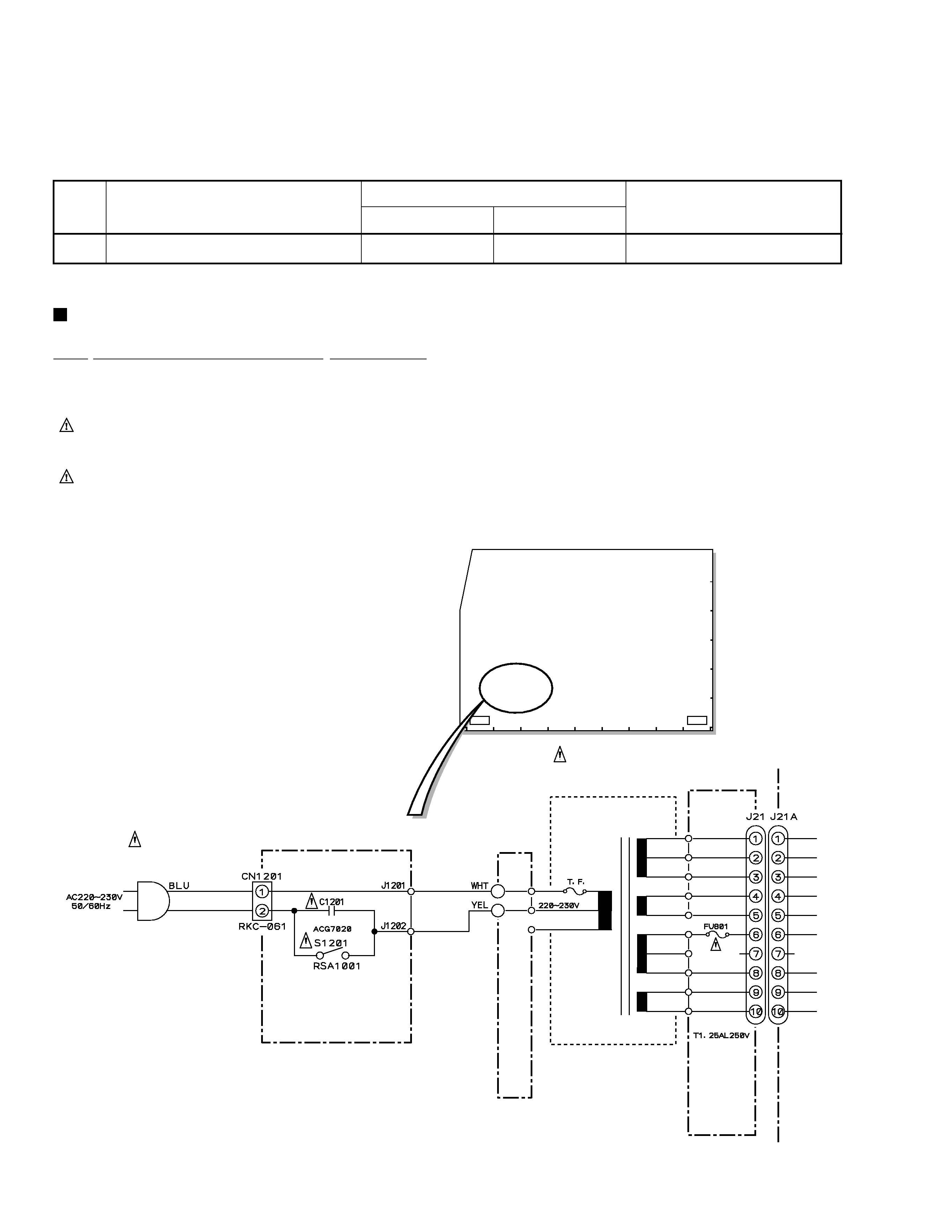
2. SCHEMATIC DIAGRAM
Note: When ordering service parts, be sure to refer to
"EXPLODED VIEWS AND PARTS LIST" or "PCB
PARTS LIST".
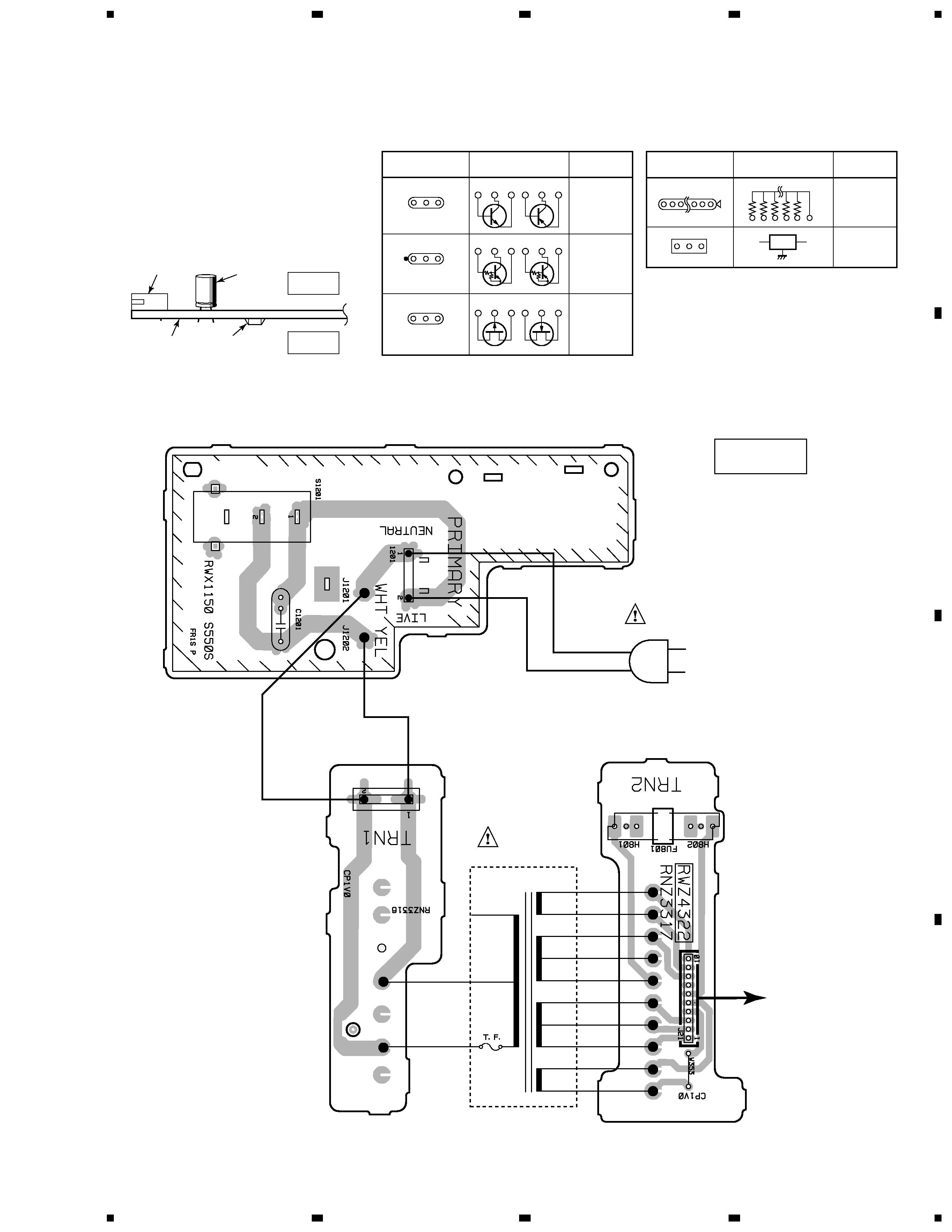
CT-S550S
5
A
B
C
D
1
23
4
1
2
3
4
NOTE FOR PCB DIAGRAMS:
1. Part numbers in PCB diagrams match those in the schematic
diagrams.
2. A comparison between the main parts of PCB and schematic
diagrams is shown below.
Symbol in PCB
Diagrams
Symbol in Schematic
Diagrams
Part Name
Transistor
Transistor
with resistor
Field effect
transistor
BC
E
BC E
BC E
DG S
BC
E
BC
E
B
C
E
DG
S D
G
S
Symbol in PCB
Diagrams
Symbol in Schematic
Diagrams
Part Name
3. The parts mounted on this PCB include all necessary parts
for several destination.
For further information for respective destinations, be sure
to check with the schematic diagram.
4. Viewpoint of PCB diagrams
Resistor array
3-terminal
regulator
Capacitor
Connector
P. C. Board
Chip Part
SIDE B
SIDE A
To MAIN UNIT
J21A
PDF1035
PDF1004
POWER TRANSFORMER
AC POWER CORD
TRN 1 PCB
POWER SW UNIT
TRN 2 UNIT
(RNP1727A)
(RNP1730A)
(RNP1730A)
3. PCB CONNECTION DIAGRAM
3.1 POWER SW UNIT, TRN 2 UNIT and TRN 1 PCB
SIDE A