© 2003-4 PRINTED IN JAPAN
B53-0050-00 (N) 3100
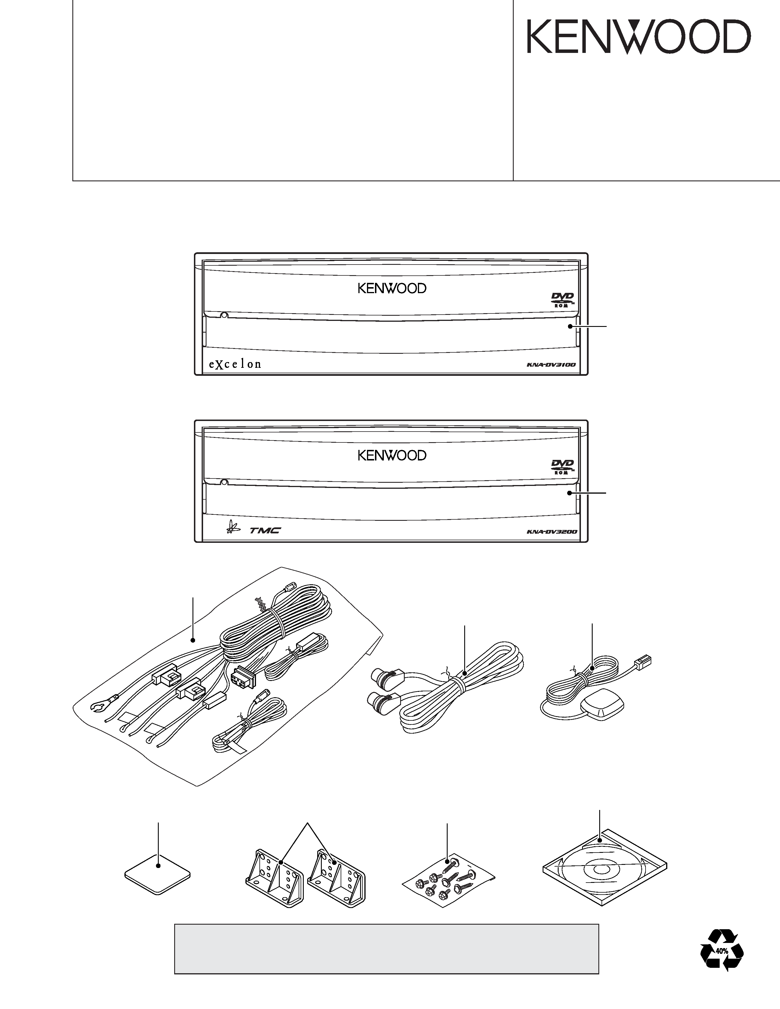
DVD NAVIGATION SYSTEM
KNA-DV3100
KNA-DV3200
SERVICE MANUAL
KNA-DV3200
KNA-DV3100
Panel assy
(A64-3105-03)
Panel assy
(A64-3106-03)
Connecting cord assy
(E30-6199-05)
Electric circuit module (GPS ANT)
(W02-3261-05)
Mounting hardware
(J21-9867-04)
Bracket
(J19-5246-04)
Screw set
(N99-1713-05)
DVD
(W01-1618-05) : KNA-DV3100
(W01-1619-05) : KNA-DV3200
DC cord assy
(E30-4964-05)
The DVD mechanism infomation is not in this sarvice manual.
Please, refer to sarvice manual X92-4740-00 (B53-0052-00).
CAUTION (Repair of NAVI board )
You can not repair IC521 (GPS Receiver) and IC701 (CORE1).
If you can repair those parts please change to NAVI board assy(W02-3395-15).
KNA-D
V3
100/D
V3200
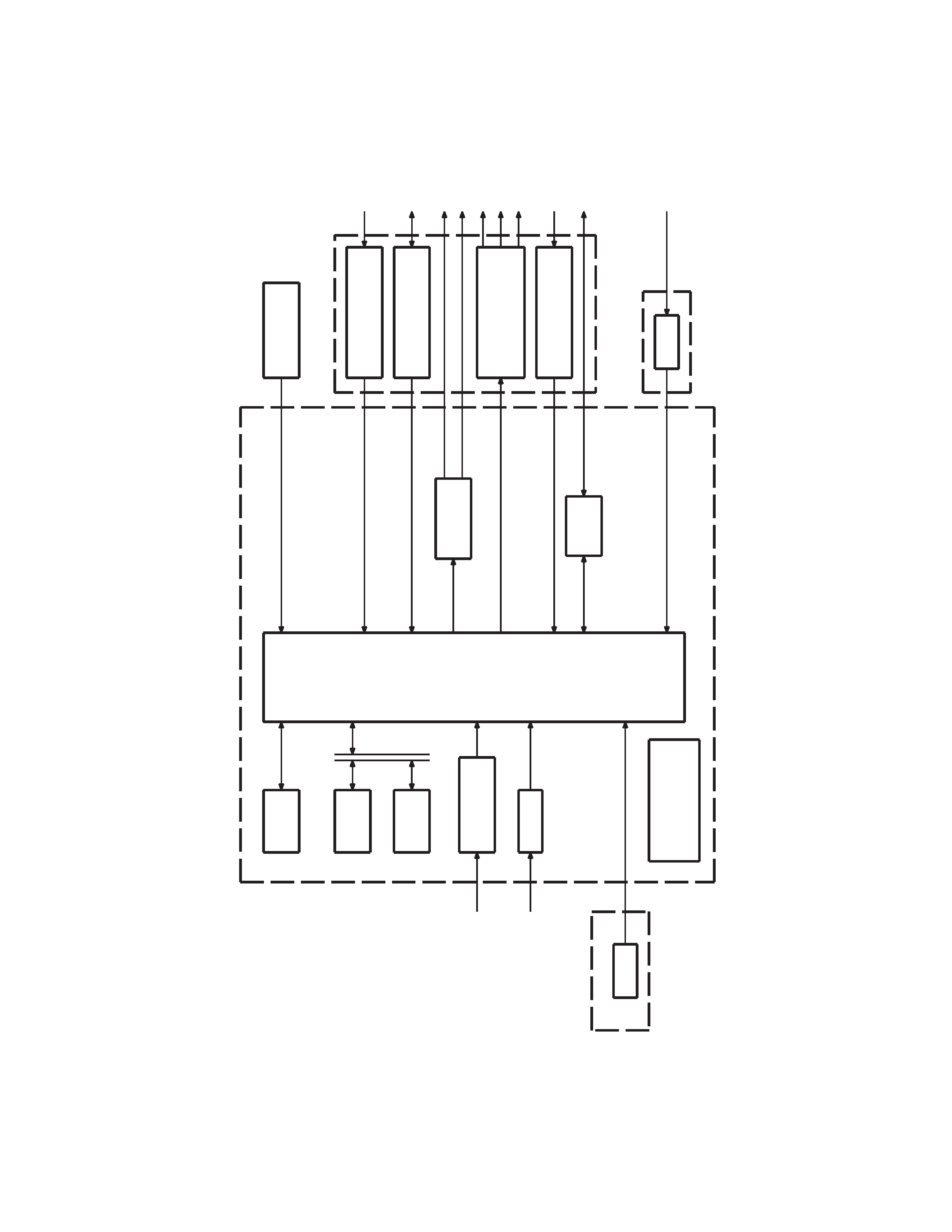
2
BLOCK
DIA
GRAM
SDRAM
64MB
FLASH
2MB
SRAM
512kB
VEHICLE
GPS RF
SPD,REV,ILL,PKB
GPS
GYRO
CORE1
A351
IC251,254,255
IC521
IC701
SIGNAL I/F
IC752-755
IC781
IC784
DVD
MECHANISM
RECOGNITION I/F
VOICE
DISPLAY
COMMUNICATION
RGB
ENCODER
OUTPUT I/F
VOICE
CONTROL
REMOTE
I/F
RS-422
SW
MIC & SW
MONITOR
MONITOR
RCA
MONITOR
RCA
ASP
TMC
RESET SW
EJECT SW
REMOTE
CONTROL
9V,8V,5V,
POWER SUPPLY
3.3V,2.5V,1.5V
IC641
IC952-956
(DIGITAL)
NAVI RGB
BEEP
NAVIVOICE
NAVI RGB
NTSC
GYRO PCB
(X25-974)
NAVI UNIT (W02-3395-05)
SUB UNIT (X89-262)
SW PCB (X25-974)

KNA-DV3100/DV3200
3
COMPONENTS DESCRIPTION
NAVI BOARD (W02-3395-15)
Ref. No.
Application/Function
Operation/Condition/Compatibility
IC101
Comparator
Voltage detected
IC102
IC
Voltage detected
IC103
SW regulator
8.3V power supply, 5V power source control
IC104
SW regulator
3.3V power supply, 1.5V power source control
IC105
3 terminal regulator
Backup 3.3V power supply
IC106
Microcomputer
Power supply, reset control
IC107
3 terminal regulator
9V power supply
IC108
3 terminal regulator
5V power supply
IC109
General purpose logic
For voltage conversion from 3.3V to 5V
IC111
General purpose logic
For mute signal generation
IC212
Point regulator
3V power supply
IC251
Non-inverter driver
Vehicle-related signal generation
IC254
General purpose logic
For SPD signal generation
IC255
Analog multiplexer
For switching vehicle speed signal
IC256
General purpose logic
For voltage conversion from 3.3V to 5V
IC301
Ope-amp
For synthesizing voice signal
IC306
Ope-amp
For voice signal for navigation system generation
IC309
General purpose logic
For voltage conversion from 3.3V to 5V
IC310
Ope-amp
For synthesizing voice signal
IC502
General purpose logic
For voltage conversion from 3.3V to 5V
IC521
RF-IC
GPS signal
IC522
Crystal oscillator
For GPS signal
IC523
Comparator
For GPS antenna detection
IC524~526
General purpose logic
For GPS signal
IC551
General purpose logic
For HDD/DVD control signal generation
IC561
General purpose logic
For EJECT signal generation
IC641
D/A converter
For video signal generation
IC642
General purpose logic
For dot clock generation
IC684
Ope-amp
For gyro sensor signal generation
IC701
Microcomputer
CORE1
IC731
3 terminal regulator
Backup 1.5V power supply
IC732,733
Point regulator
2.5V power supply
IC734
3 terminal regulator
1.5V power supply
IC751
Analog switch
For CKE signal generation
IC752~755
128M-SDRAM
16MB
IC781
4M-SRAM
512MB
IC782,783
General purpose logic
For generating CS signal
IC784
16M-FLASH
2MB
IC951
Line transceiver
RS422/TMC transceiver
KNA-DV3100/DV3200
4
Ref. No.
Application/Function
Operation/Condition/Compatibility
IC952
General purpose logic
For generation of TMC control signal
IC954~956
General purpose logic
For generation of TMC control signal
IC957
General purpose logic
For mute signal generation
T101
Transistor
Power ON/OFF control
T102
Power MOS FET
Power ON/OFF control
T103,104
Transistor with resistor
For T101&T102 control
T105,106
Transistor
DC/DC switching
T107,108
Power MOS FET
Power ON/OFF control
T109
Transistor with resistor
For delayed ACC control
T110,111
Transistor
DC/DC switching
T112,113
Transistor
For backup 3.3V power supply control
T305
Transistor array
For control navigation system voice mute
T306
Transistor array
For control LMUTE
T307
Transistor with resistor
For control beep volume
T309
Transistor with resistor
For control beep volume
T319
Transistor with resistor
For control T305
DAUGHTER UNIT (X89-2622-71)
Ref. No.
Application/Function
Operation/Condition/Compatibility
IC1
Power supply IC
5V power supply for ACTIVE SP
IC2
AND gate
Buffer for TV communicatioin (TX/RX) signal
IC3
MIC amplifier
Isolation amplifier for external microphone
IC4
NAND gate
For switching remote control signal (TV/Remoto control sensor)
Q1,2
Driver
Mute driver
Q3
Buffer
TV SYNC signal buffer
Q4
Buffer
ACTIVE SP signal buffer
Q5
Mute switch
RCA (Voice) Rch mute switch
Q6
Mute switch
ASP (Voice) mute switch
Q7
Mute switch
RCA (Voice) Lch mute switch
Q8
Mute switch
TV (Voice) Lch mute switch
Q9
Mute switch
TV (Voice) Rch mute switch
COMPONENTS DESCRIPTION

KNA-DV3100/DV3200
5
MICROCOMPUTER'S TERMINAL DESCRIPTION
MICROCOMPUTER : MB89935B (NAVI BOARD : IC106)
Pin No. Pin Name I/O
Function
Processing Operation Description
1
P04
O
FRES output
Lo : Flash ROM and CORE1 reset
2
P05
O
RES output
Lo : System reset
3
P06
O
NMI output
Interrupt output to CORE1
4
P07
I
Not used (Pull down to GND line)
5
MODE0
I
Mode input 0
Lo Fixed (Connect to GND Line)
6
MODE1
I
Mode input 1
Lo Fixed (Connect to GND Line)
7
RST#
I
Reset input
Lo : At the time when system is down and when panel reset SW is pressed
8X0-
Clock oscillator terminal
9X1-
Clock oscillator terminal
10
VSS
-
GND connection terminal
Connect to GND line
11
P37
O
P ON terminal
Hi : Turning power ON for SW's system power circuit
12
P36
I
WDP input
Detection of watchdog pulse from CORE1
Normal operation : Logic is reversed within 300ms
13
P35
I
ACC detection input
Hi : ACC ON
14
P34
I
BU detection input
Hi : BU ON
15
P33
I
SDRAM clock enable input
Lo : Self-refresh of SDRAM, Hi : Normal operation of SDRAM
16
C
-
C connection terminal
(0.1
µF)
17
P32
I
Not used (Pull down to GND line)
18
P31
I
Delayed ACC input
Hi : CORE1 in operation and panel mechanism in operation when ACC is OFF
19
P30
O
ACC detection output
Hi : Power ON, Lo : Power OFF (Output to CORE1 and system computer)
20
P50
O
Backup operation complete notice
Hi : SDRAM CKE core in control, Lo : Backup processing complete
21
AVSS
-
GND connection terminal
Connect to GND line
22
P40
O
V33D switching output
Lo : Normal (ACC ON)
23
P41
O
V33D switching output
Lo : At the time of backup
24
P42
O
Mute output
Lo : Mute
25
P43
I
V33 monitor input
Lo : No Output
26
P00
I
VMAIN monitor input
Lo : No Output
27
P01
I
BU monitor input
Lo : No BU
28
P02
I
V50 output monitor input
Lo : No Output
29
P03
I
V80 output monitor input
Lo : No Output
30
VCC
-
Positive power supply terminal
Connect to 3.3V line backup