70%
MULTIPLE DVD/VCD/CD PLAYER
DV-605/DVF-R5060-S
SERVICE MANUAL
© 2002-7 PRINTED IN KOREA
B51-5802-00 (K/K) 1402
In compliance with Federal Regulations, following are repro-
duction of labels on, or inside the product relating to laser
product safety.
KENWOOD Corp. certifies this equipment conforms to DHHS
Regulations No.21 CFR 1040. 10, Chapter 1, subchapter J.
DANGER : Laser radiation when open and interlock defeated.
AVOID DIRECT EXPOSURE TO BEAM.
Caution : No connection of ground line if disassemble
the unit. Please connect the ground line on
rear panel, PCBs, Chassis and some others.
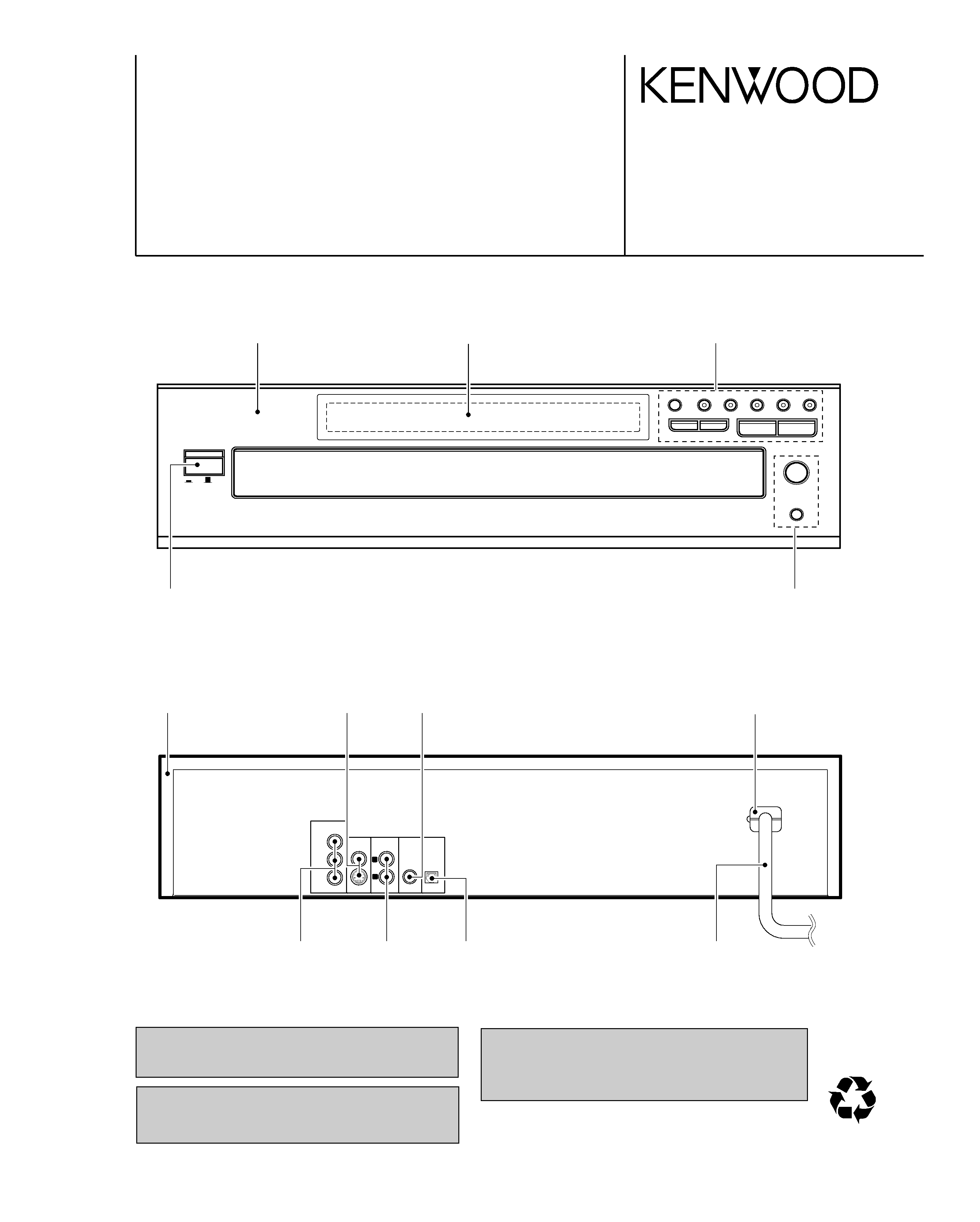
76
0
POWER
ON
OFF
4
¢
DISC SKIP
SEQUENCE
MODE
DISC 1
DISC 2
DISC 3
DISC 4
DISC 5
AUDIO
OUTPUT
VIDEO
OUTPUT
S-VIDEO
OPTICAL
COAXIAL
L
R
COMPONENT
VIDEO OUTPUT
Cr
Cb
Y
Cabinet panel *
(A60-)
Crystal Window *
(B10-)
DIN socket
(E68-0018-08)
Top cover *
(A01-)
Button *
(K29-)
Button *
(K27-)
Knob(POWER) *
(K27-)
Phono socket
(E63-1244-08)
AC power cord bushing
(J42-0350-08)
AC power cord
(E30-7250-08)
Phono socket
(E63-1227-08)
Oscillating module
(GP1F32T)
Phono socket
(E63-1192-08)
* Refer to parts list on page 19.
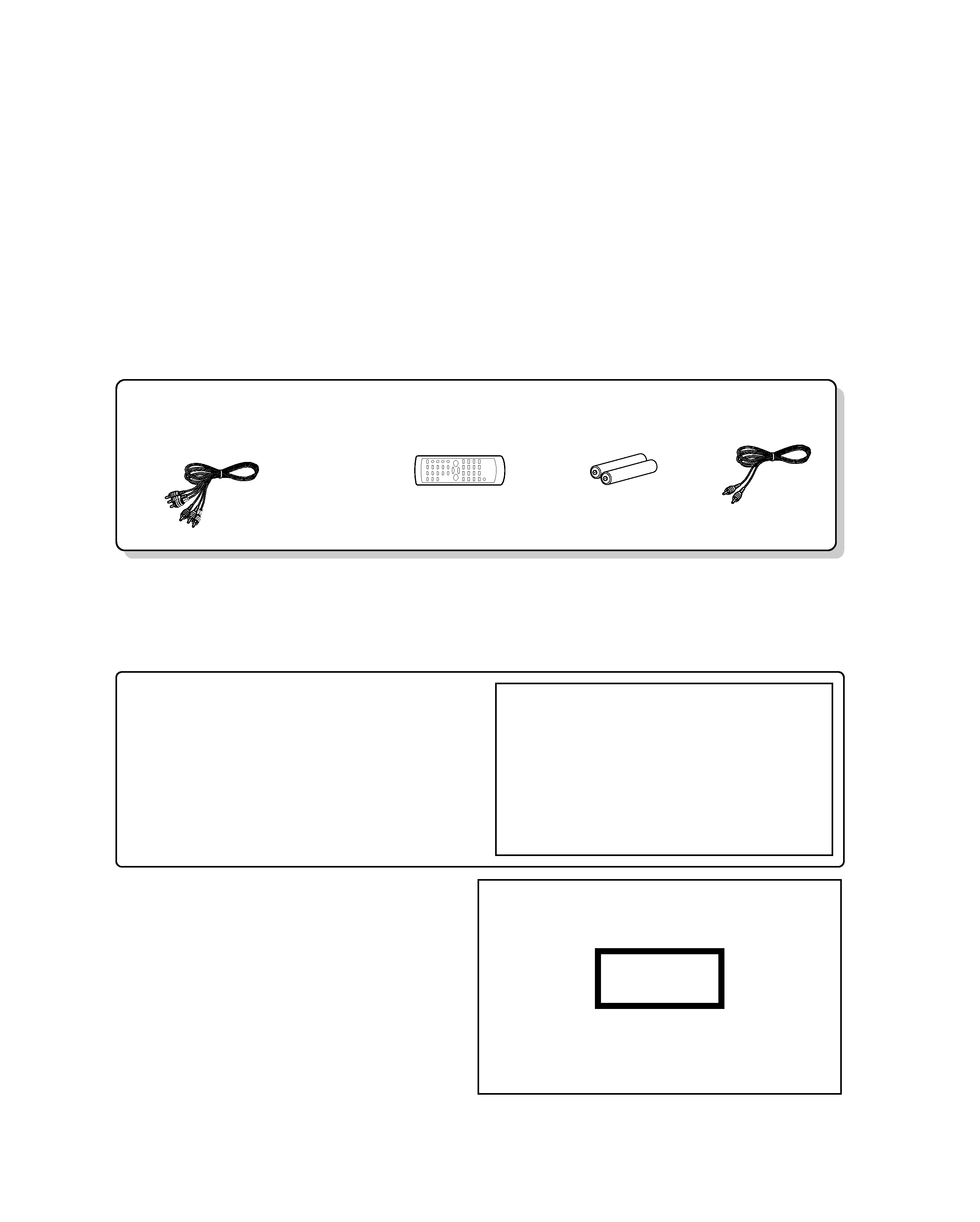
Batteries(R6/AA) ...(2)
Please confirm that the following accessories are present.
Audio video cord (Red, White, Yellow) ...(1)
(E30-2990-08)
Remote control unit ...(1)
(A70-1570-08)
Coaxial cable ...(1)
(E30-7235-08)
DV-605/DVF-R5060-S
2
CONTENTS / ACCESSORIES / CAUTIONS
CONTENTS / ACCESSORIES / CAUTIONS ............. 2
DISASSEMBLY FOR REPAIR....................................3
BLOCK DIAGRAM ......................................................4
ADJUSTMENT ............................................................4
PC BOARD ................................................................ 5
SCHEMATIC DIAGRAM .......................................... 11
EXPLODED VIEW ....................................................17
PARTS LIST..............................................................19
SPECIFICATIONS ......................................Back cover
Contents
Accessories
Cautions
The marking of products using lasers
(For countries other than U.S.A., U.S.-Military and Canada)
The marking this product has been classified as Class 1. It
means that there is no danger of hazardous radiation outside
the product.
Location: Back panel
CLASS 1
LASER PRODUCT
Operation to reset
÷ Please note that resetting the microprocessor clears the
contents stored in, it returns the microprocessor to the con-
dition when it left the factory.
1 In Power ON condition, keep the DISC 3 key and the 4
(Skip) key pressed at the same time.
2 When both keys are pressed, the region code of the unit,
the software version, etc. will be displayed on the dis-
play. (When nothing is done, the display of this informa-
tion continues.) Example: 72. 14.02:05
3 Press the DISC 4 key and the 4
4
4
4
4 key at the same time.
"BYE" will be shown on the display.
4 Press the POWER ON/OFF switch to go to Power OFF.
5 When Power ON is performed with the POWER ON/OFF
switch, the settings become the default factory settings.
The microprocessor may fall into malfunction (impos-
sibility to operate erroneous display, etc.) when the
power cord is unplugged while power is ON or due to
an external factor. In this case, execute the following
procedure to reset the microprocessor and return it to
normal condition.
DV-605/DVF-R5060-S
3
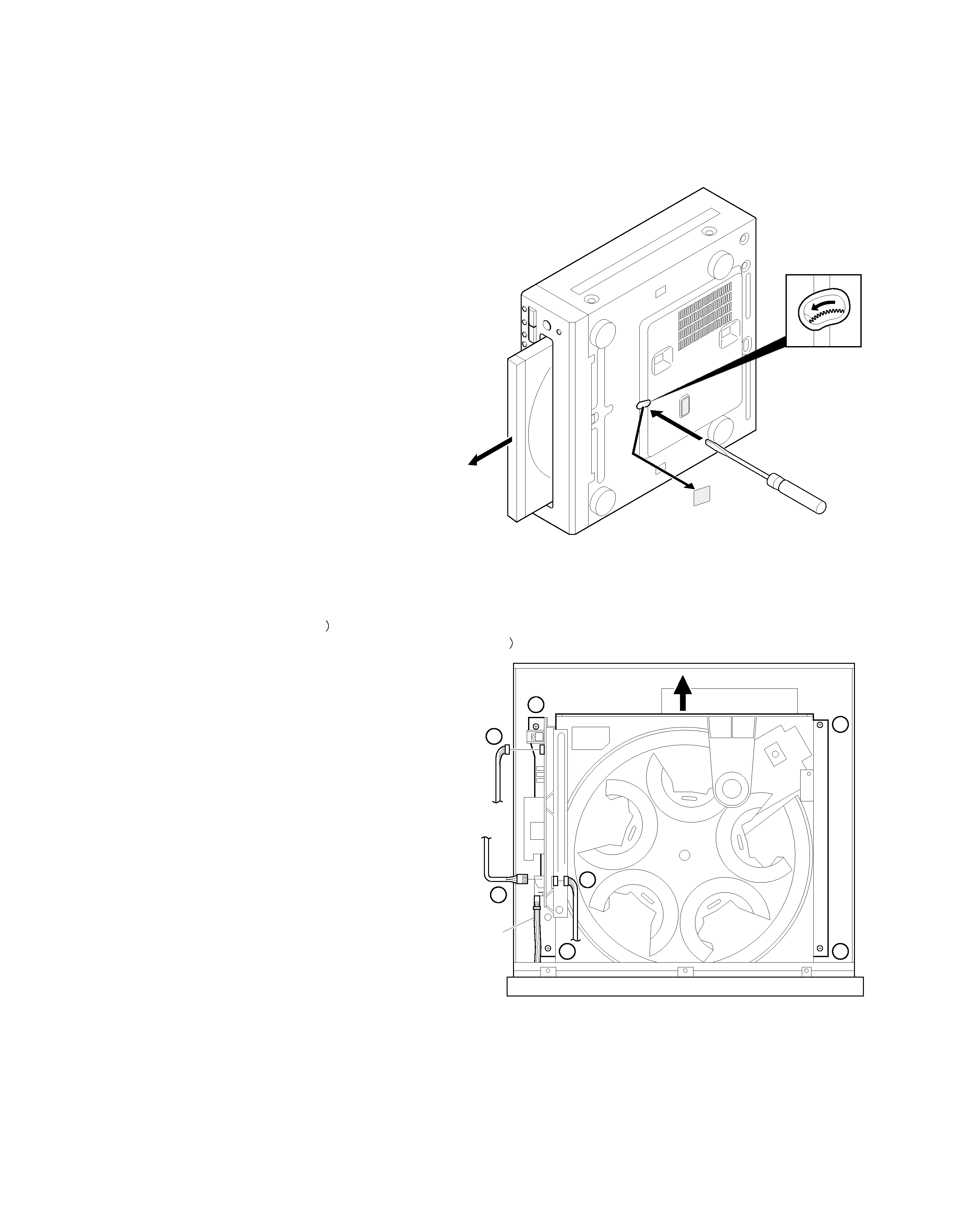
DISASSEMBLY FOR REPAIR
1. How to open the tray if it does not come out.
(Fig.1)
1. Remove the plastic plate.
2. Turn the gear fully CCW using a flat driver and so on in the
drawing through the hole on the loading chassis bottom.
3. Pull out the tray frontward by hand when it comes just out.
2. How to remove the DVD mechanism. (Fig.2)
1. Remove connectors (
1~3 and power switch lever.
2. To separate the DVD mechanism, remove screws (
4x4
and pull it out backward.
PLASTIC
PLATE
2
3
4
4
4
4
1
POWER
SWITCH
LEVER
Fig. 1
Fig. 2
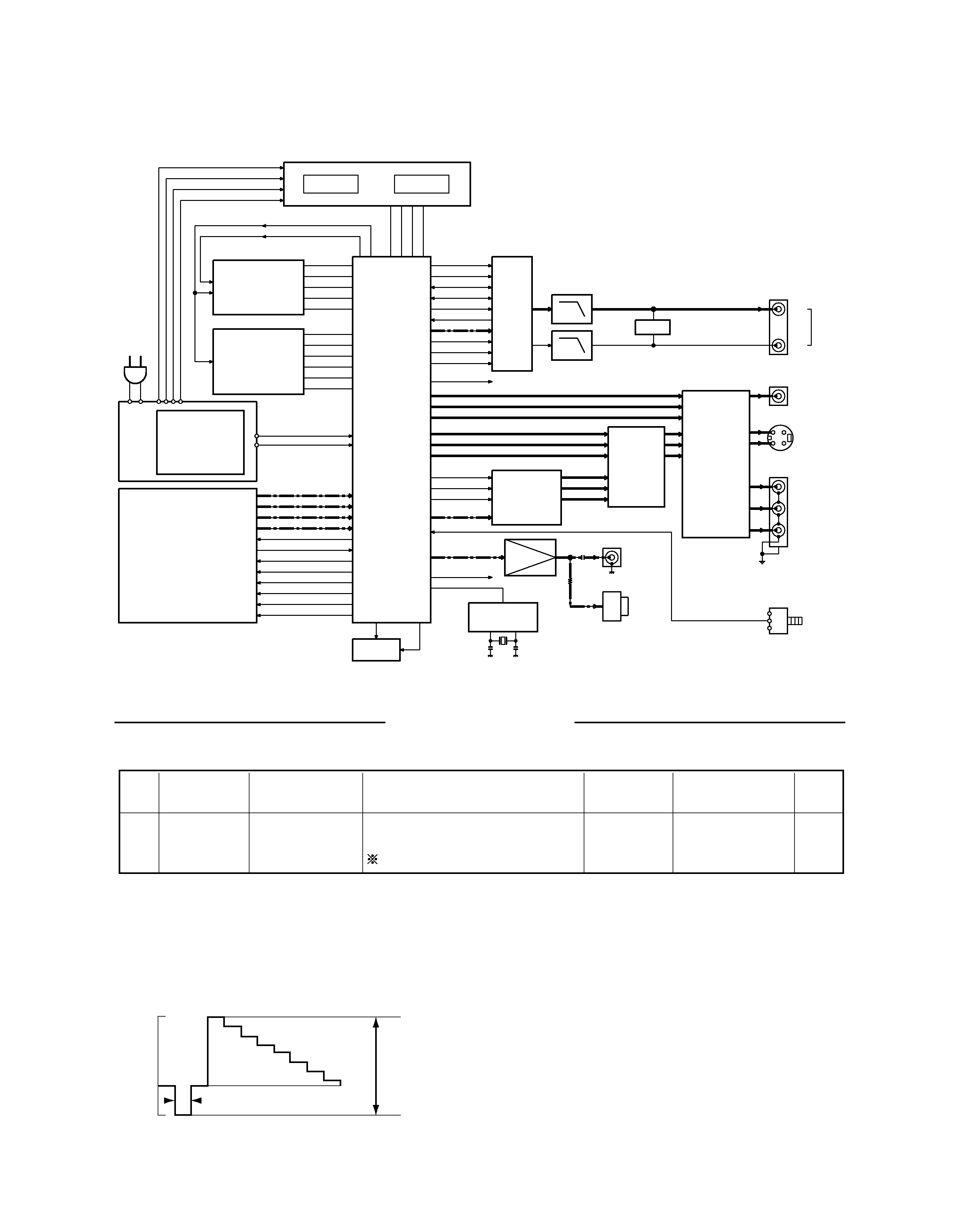
+5VS
FL AC
FL AC
-27V
ADDR+
F-WE
F-DE
F-RESET
ADDR+
D-RAS0-
RDNOTWR
DATA+
D-CAS0-
D-CAS1-
F-CE
F-OE(DRAM OE)
+5V6S
TXD
RXD
RESET
MAIN
IRQ2
+3V3-RESET
EXIT-DATA
EXIT-BCLK
EXIT-DATAVALID
EXT-PSTART/ERROR
F/E SDATA
+9V MOTOR VCC
+9V MOTOR VCC
+3.3V DIGITAL VCC
+5V DIGITAL VCC
F/E SCL
PCM-DATA
DAC LATI25
DAC SCKDSD
DAC SDIDEM
DAC MUTEB
CSBWL
PCM MCLK
PCM LRC
PCMCLK
AUDIO MUTE
CVBS-OUT
Y-OUT
C-OUT
I (Y)-OUT
I (Y)-OUT
I (Y)-OUT
P (Cr)-OUT
P (Cb)-OUT
P (Y)-OUT
P SCAN CLK
P SCAN DATA
P SCAN STB
VIA2-VIA8
GND
SPDIF
VIDEO MUTE
PIXCLK-27MHZ
SDA
SCL
L AUDIO
R AUDIO
F-OE(DRAM
OE)
DAC ZERO
DATA+
AC CORD
+9V ANALOG VCC
-9V ANALOG VCC
+5V DIGITAL VCC
+3.3V DIGITAL VCC
+9V MOTOR VCC
5V FRONT
IC91
FL
M29F400T-90N1
8MBIT
FLASH MEMORY
IC41
HY57V651610BLTC-8
SDRAM-64MBIT
IC31
125MHz
IC21
MPEG
STI5519
IC61
DAC
WM8728
L.P.F
L.P.F
BA4560
MUTE
JK82
Lch
Rch
MIXED
IC11
PM0026
PROGRASSIVE
I/P
TR
DRIVER FOR
75 ohm x2
IC12
PROGRASSIVE
6CH/6dB/FOR
MM1568
DVD
SWITCHING
CVBS-VIDEO
JK83A
JK83B
S-VIDEO
Y
JK84
Cr
Cb
RCA 3V
JK87
ON/OFF
P SCAN
SW
BUFFER
COAXIAL
JK81
OPTICAL
IC85
IC51
74HCU04
HEX INVERTER
IC22
EEPROM
M24C02
Q61R
Q61L
SMPS
TVM MECHA
F/E & MECHA
DV-605
DV-605/DVF-R5060-S
4
BLOCK DIAGRAM
ADJUSTMENT
No.
ITEM
INPUT SETTING
OUTPUT SETTING
ALIGNMENT
POINT
ALIGNMENT
FOR
FIG.
1
Progressive
Y LEVEL
100% COLOR
BAR DISC
Connect the oscilloscope to
Y output(JK84) with 75-ohms resistor.
Output Mode: Progressive
VR11
Y-signal=
1000mV
±100mV
FIG.1
1000mV
±100mV
Y
4.7
µs
-286
0
714
(100IRE)
[mV]
white
yellow
cyan
green
magenta
red
blue
black
714
641
516
443
324
252
127
54
Fig. 1
Adjustment Method & Precautions
1. Play Back 100% White Pattern
2. Channel 2 : OSC Probe, Composite(JK83-A)
3. Channel 1 : OSC Probe, Y(JK84) output
Channel 2 : Trigger
4. OSC Time / Div Control
5. VR11Variable : See the Scope Wave
DV-605/DVF-R5060-S
5
CIRCUIT DESCRIPTION
Pin No.
Pin Name
I/O
Pin Description
PIOs and communication
1
PIO2(5) DAC SDIDEM IN/OUT
I/O DAC data input and output.
2
PIO2(6) DAC MUTEB IN/OUT
I/O DAC mute control.
3
PIO2(7) DAC CSBIWL OUT
O
DAC chip select.
6
PIO3(0) PRO SCAN ON/OFF
I
P. Scan switch input.
7
PIO3(1)
I/O Unused.
8
PIO3(2)
O
PROG-H
9
PIO3(3)
O
PM0026A (IC11) Clock
10
PIO3(4) IR REMOCON
I/O IR Remote controller signal output (Unused).
11
PIO3(5)
O
PM0026A (IC11) data
12
PIO3(6)
O
PM0026A (IC11) STB
13
PIO3(7) DVD RESET
I/O Power- on reset of front-end module.
Front-end
16
B DATA
I
I2S Data
17
B BCLK
I
I2S Bit clock
18
B FLAG
I
I2S Error flag
19
B SYNC
I/O I2S Sector / ABS time
Reserved
20
B WCLK
I/O Unused.
21
B V4
I/O Unused.
22
NRSS OUT
I/O Unused.
23
VDD RGB
-
Supply voltage for RGB (+2.5VA).
24
VSS RGB
-
GND
Video DAC
25,26,27
B/G/R (OUT)
O
B/G/R signal outputs.
28
V REF RGB
I
Reference voltage input for DAC RGB.
29
I REF RGB
I
Reference current input for DAC RGB.
30
VDD YCC
-
Supply voltage for YCC (+2.5VA).
31
VSS YCC
-
GND
32~34
Y/C/CV (OUT)
O
Y/C/CV signal outputs.
35
V REF YCC
I
Reference voltage input for DAC YCC.
36
I REF YCC
I
Reference current input for DAC YCC.
PIOs and communication
39~46
PI04(0~7)
I/O YC(0~7)
Audio DAC
48
VDD PCM
-
Supply voltage for PCM (+2V5).
49
VSS PCM
-
Ground for PCM.
51
DAC SCLK (BCK)
O
DAC over sampling clock.
52
DAC PCMOUT0 DATA
O
DAC PCM data out 0.
53
DAC PCMOUT1
O
DAC PCM out 1 (unused).
54
DAC PCMOUT2
O
DAC PCM out 2 (unused).
55
DAC PCMCLK
O
DAC PCM clock.
56
DAC LRCLK
O
DAC PCM Left/Right clock.
57
SPDIF OUT
O
Audio digital data output.
Shared memory interface
66~69
SMI ADR(3~0)
O
SDRAM address bus.
58~63
SMI ADR(4~9)
O
SDRAM address bus.
70~73
SMI ADR(10~13)
O
SDAM address bus.
74
SMI CS(0)
O
Chip select bank 0.
75
SMI CS(1)
-
Unused.
76
SMI RAS
O
SDRAM RAS
77
SMI CAS
O
SDRAM CAS
78
SMI WE
O
SDRAM write enable.
79
SMI DQML
O
DQ MASK enable low.
1. Pin Description of MPEG Processor (Main, IC21)