COMPACT DISK PLAYER
DP-SE7/SE7(G)/SE9
SERVICE MANUAL
©1997-10/B51-5371-00 (K/K) 3191
6
0
repeat
7
¢
4
1
¡
time
space
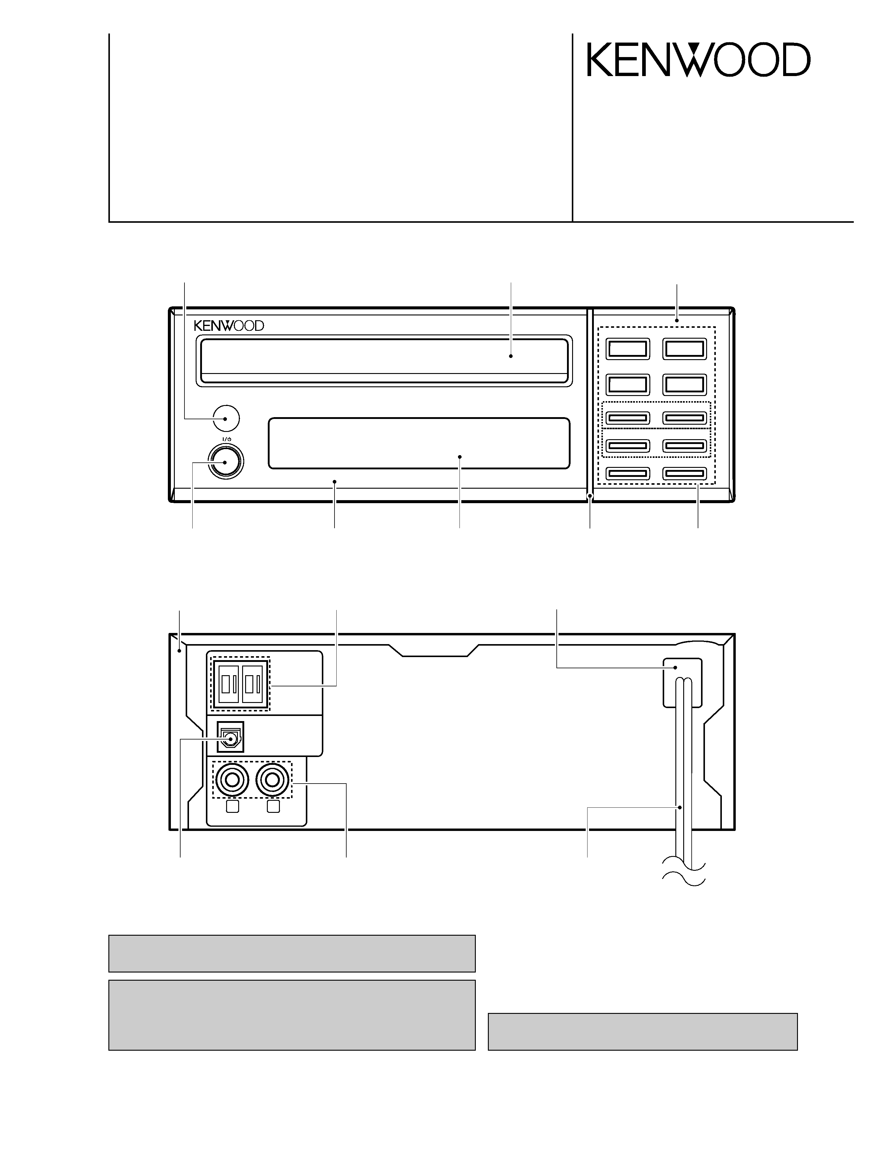
compact disc player
DP-SE7
on/standby
D.R.I.V.E.
'
OPTICAL
SYSTEM
CONTROL
DIGITAL OUT
PLAY OUT
R
L
Indicator
(B12-0318-04)
Panel *
(A60-)
Front glass
(B10-2372-03)
Panel
(A29-0872-03)
AC power cord *
(E30-)
Oscillating module
(W02-1114-05)
Phono jack
(E63-0122-05)
Metallic cabinet
(A01-3321-01)
Power cord bushing
(J42-0083-05)
Rectangular receptacle
(E08-0312-05)
Knob
(K29-6744-04)
Escutcheon
(B07-2363-04)
Knob
(K29-6743-03)
Panel *
(A60-)
(HM-701)
Illustration is DP-SE7Mtype.
* Refer to parts list on page 17.
In compliance with Federal Regulations, following are reproductions of
labels on, or inside the product relating to laser product safety.
KENWOOD-Crop. certifies this equipment conforms to DHHS Regulations
No. 21 DFR 1040. 10, Chapter 1, Subchapter J.
DANGER : Laser radiation when open and interlock defeated.
AVOID DIRECT EXPOSURE TO BEAM
Refer to DP-SA7 service manual (B51-5243-00) if you require
Disassembly for repair in detail.
DP-SE7(G)/SE9(K) COVER( 97.11.2711:26PM y[W 2
DP-SE7/SE7(G)/SE9
CONTENTS / EXTERNAL VIEW
2
CONTENTS / EXTERNAL VIEW ............................... 2
CIRCUIT DESCRIPTION ............................................3
ADJUSTMENT ............................................................6
PC BOARD ................................................................ 7
SCHEMATIC DIAGRAM ............................................ 9
EXPLODED VIEW ....................................................15
PARTS LIST..............................................................17
SPECIFICATIONS ......................................Back cover
Contents
System configuration
SYSTEM NAME
RECEIVER
CD PLAYER
SPEAKER
HM-701
R-SE7
DP-SE7
LS-SE7
HM-901
R-SE9
DP-SE9
LS-SE9
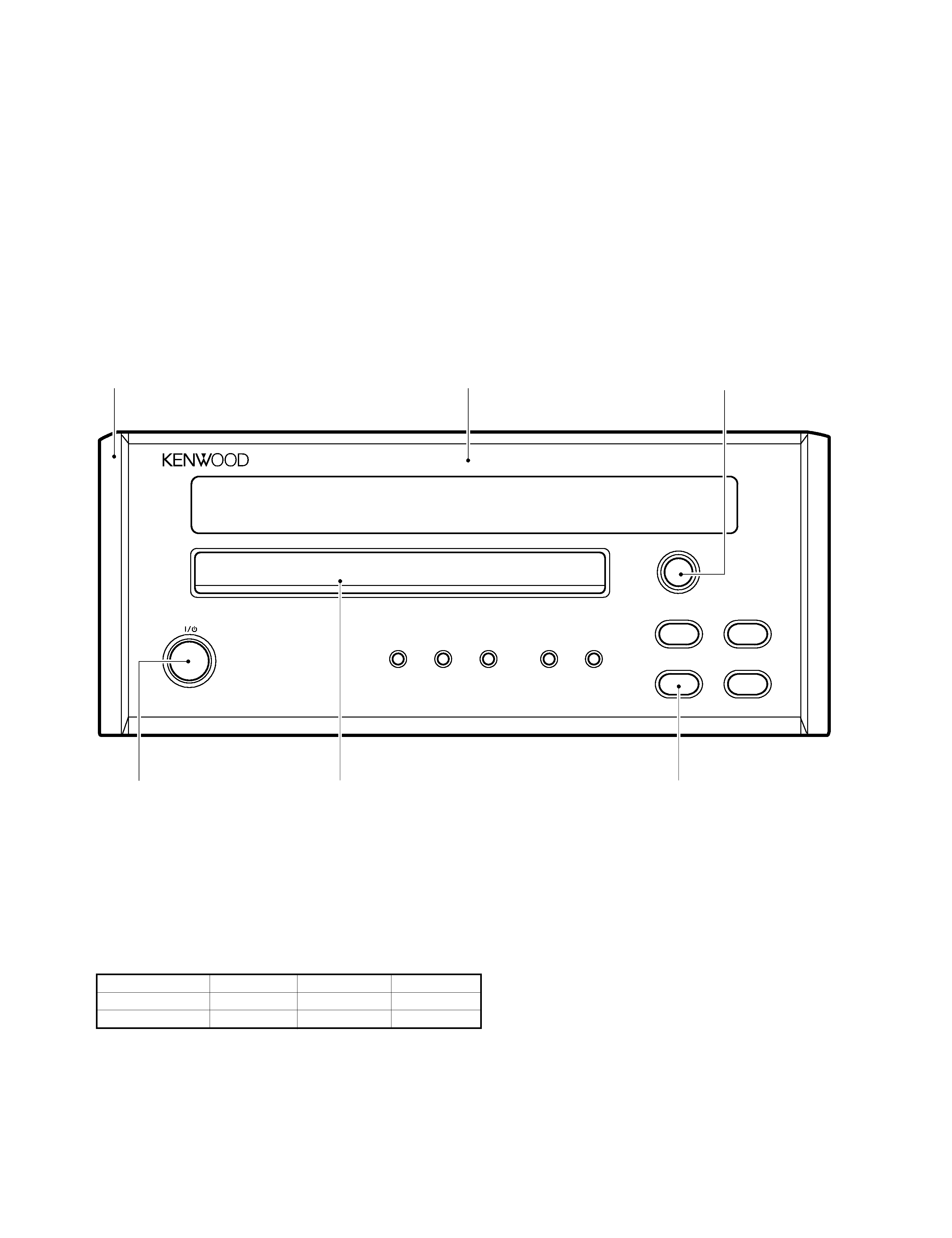
compact disc player
on/standby
time
space
repeat
1
¡
0
7
4
¢
6
24 bit fine D.R.I.V.E.
D.R.I.V.E. with 24 bit D/A conversion
'
DP-SE9
Side plate
(A50-1303-12)
Panel
(A29-0871-03)
Panel
(A60-1266-02)
Knob
(K29-6741-04)
Knob
(K29-6766-04)
Knob
(K29-6742-04)
Illustration is DP-SE9.
DP-SE7(G)/SE9(K) COVER( 97.11.2711:26PM y[W 3
DP-SE7/SE7(G)/SE9
3
CIRCUIT DESCRIPTION
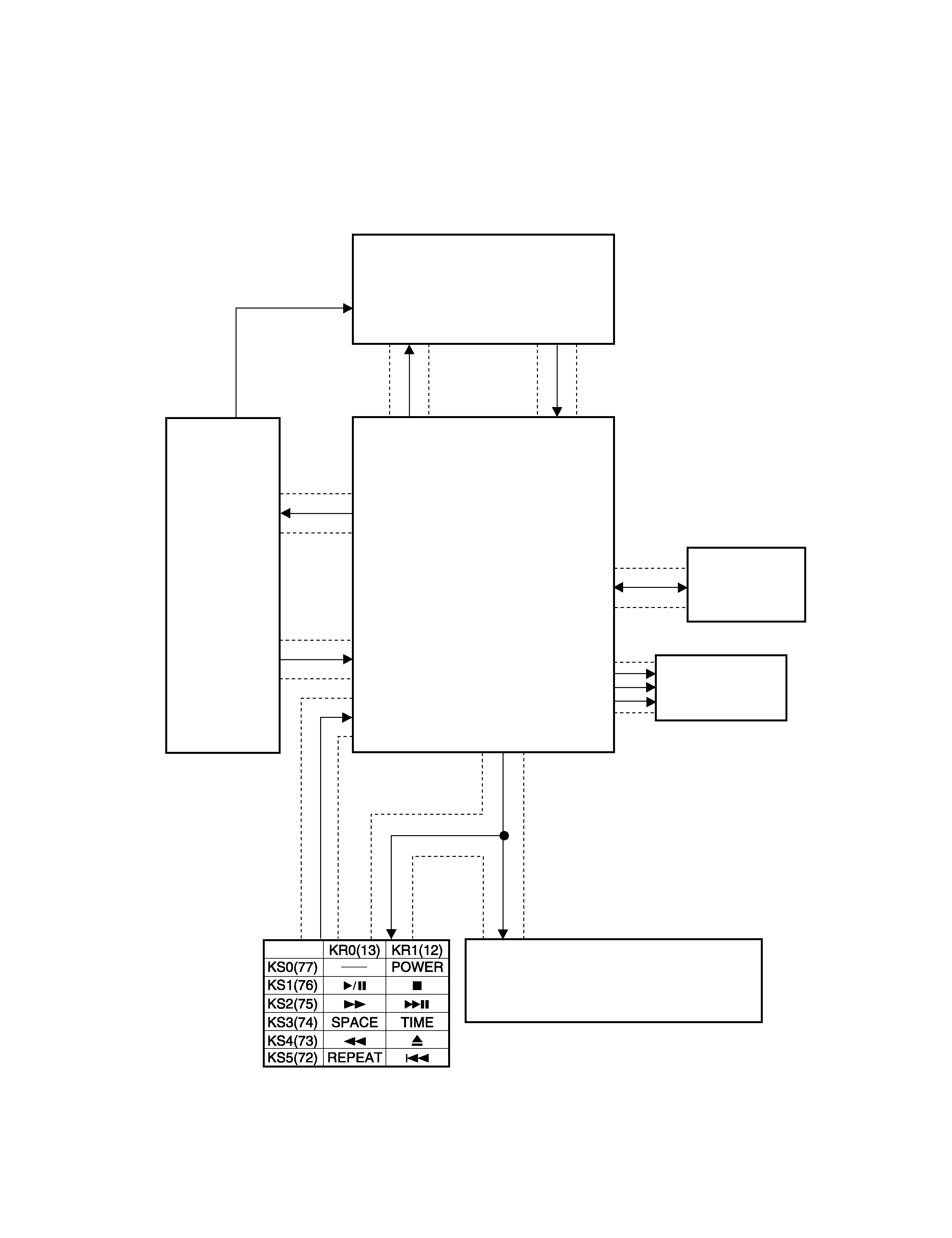
(X32) IC2
KAN03
213BGN
8-BT-207GK
µPD78044FGF
SDATA
SBUSY
(X25) IC5
CLK, DTA, LAT
S. CLK M. ON
MUTE XLON
SENSE
SCOR
SUBQ
(SLTSW)
(FOK , GFS)
SGATE
SCK
SDT
KR0,KR1
SLT SW
Seg key scm pin
KSL-
CD mecha
MOTOR CONTROL
TERMINAL
SWITCH INPUT
X 2
KEY INPUT
X 2
GRID X 8
SEGMENT X 12
SYSTEM
SERIAL
SIGNAL
D.S.P.
CXD 2507AQ
6
KEY MATRIX
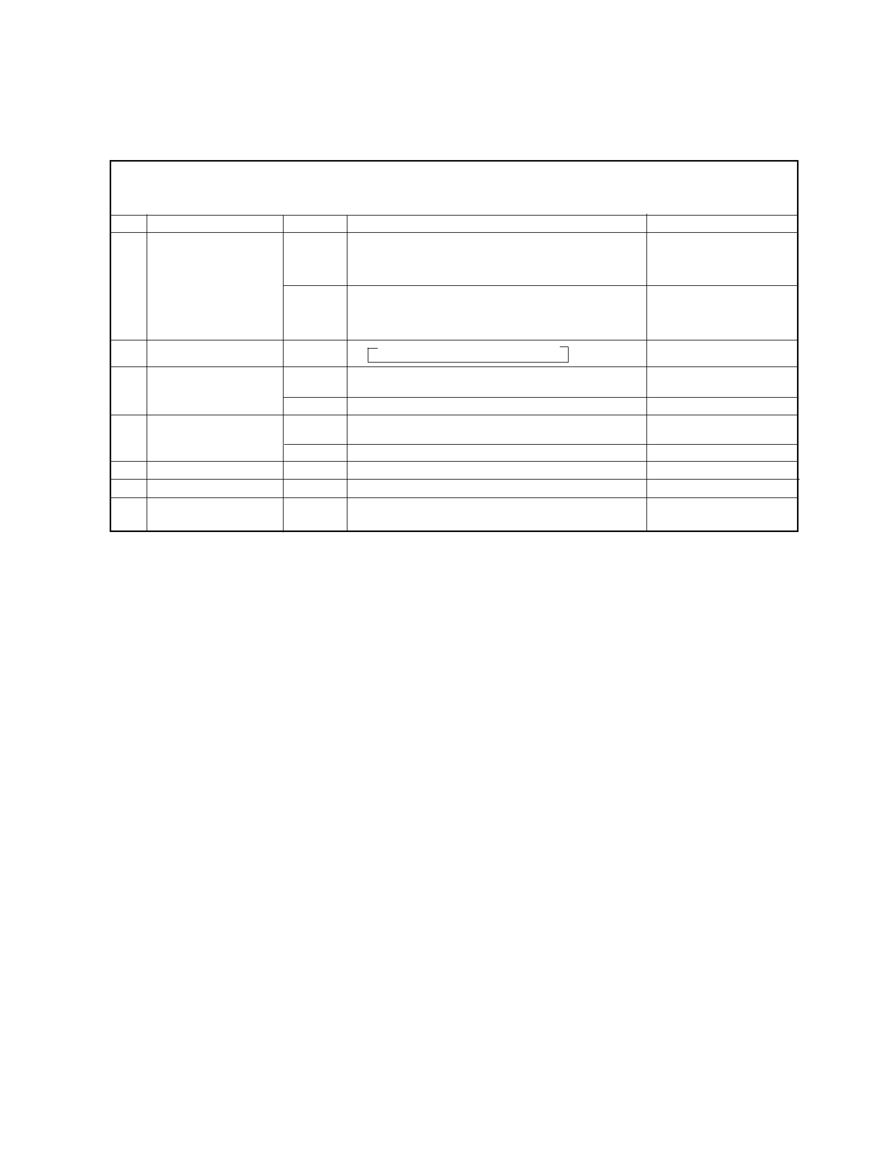
1. Microprocessor
1-1. Microprocessor periphery block diagram
DP-SE7(G)/SE9(K) COVER( 97.11.2711:26PM y[W 6
DP-SE7/SE7(G)/SE9
4
CIRCUIT DESCRIPTION
PIN No.
PIN NAME
I/O
DESCRIPTION
1~7
Grid 2G~8G
O
FL Digit control (Grid 2G~8G)
8
Vdd
O
Power supply (+5)
9
SQCK
O
Q-data read clock output.
10
STBY
O
Not use (OPEN)
11
SUBQ
I
Q-data (or SLT SW) input
12
KR 1
I
Key return input 1
13
KR 0
I
Key return input 0
14~16
NC
I
Not use (PULL DOWN)
17
RESET
I
Reset input
18, 19
NC
I
Not use (PULL DOWN)
20
AVss
Not use (GND)
21~24
NC
I
Not use (PULL DOWN)
25
SDT
O
Enable output to KAN03
26
SCK
O
Clock output to KAN03
27
S GATE
O
Data output for KAN03
28
NC
I
Not use
29
AVdd
Not use (+5V)
30
AVref
Not use (GND)
31
DEFECT
I
Scratch disk compel sat
32
XT2
Not use (OPEN)
33
Vss
GND
34
X1
I
System clock
35
X2
System clock
36
RMUTE
O
Analog mute
37
CLK
O
CXD2507AQ clock output
38
LATCH
O
CXD2507AQ latch output
39
DATA
O
CXD2507AQ data output
40
SENSE
I
SENSE/GFS/F.OK input
41
D.S
O
Not use
42
S.DATA
I/O
Serial DATA I/O
43
S.BUSY
I/O
Serial BUSY I/O
44
SCOR
I
Sub-code synch detect
45
NC
I
Not use (PULL DOWN)
46
M.ON
O
Focus lock compensation
47
REMOCON
I
REMOCON
48
Vpp
GND
49
CLOSE SW
I
Tray close (L : close)
50
OPEN SW
I
Tray open (L : open)
51
NC
I
Not use (PULL DOWN)
52
Vdd
Power supply (+5V)
53
OPEN MOTOR
O
Motor [OPEN] (H : OPEN/T.U.DOWN)
54
CLOSE MOTOR
O
Motor [CLOSE] (H : CLOSE/T.U.UP)
55~64
NC
O
Not use (OPEN)
65~70
Sa~Sf
O
FL Segment (SEG Sa~Sf)
71
Vlord
FL driver power supply (-30V)
72~77
SEG Sg~Sl/KS 5~0
O
FL Segment Sg~Sl and key scan (KS5~KS0)
78, 79
NC
O
Not use (open)
80
GRID 1G
O
FL digit (Grid 1G)
1-2 Pin description
(uPD78044FGF-071 : X25, IC4)
DP-SE7(G)/SE9(K) COVER( 97.11.2711:26PM y[W 7
5
DP-SE7/SE7(G)/SE9
CIRCUIT DESCRIPTION
MODE "0 0" : Use for Test or alignment
Setting the test mode : While pressing the "REPEAT" key, plug the AC cord
into wall output.
No.
Key
Display
Operation
Remarks
(1)Focus servo .........................................ON
03
(2) Tracking servo ....................................OFF
TE-adjustment
1
PLAY/ PAUSE
(3) Feed servo .........................................OFF
6
(1) Focus servo.........................................ON
F-GAIN / T-GAIN
05
(2) Tracking servo.....................................ON
(3) Feed servo ..........................................ON
FE-B adjustment
2
UP
¢
All display ON
= All display OFF
01
Pick manual feed (outside
= inside)
Stop mode only
3
FB
1
05
FB operation is available
Time display goes off
4
FF
¡
01
Pick manual feed(inside
= outside)
Stop mode only
05
FF operation is available
Time display goes off
5
STOP
7
01
Pick-up initialize
6
OPEN / CLOSE
0
Tray open / close
7
DOWN
4
01
Cancel the test mode, and
Play track No.01
return to normal mode.
2. Test mode
PCB/EXP 97.11.27 8:11 AM y[W 1