SERVICE MANUAL
PORTABLE MINIDISC PLAYER
No.20738
Jan. 1999
COPYRIGHT
1999 VICTOR COMPANY OF JAPAN, LTD.
Printed in Japan
9901 (V )
VICTOR COMPANY OF JAPAN, LIMITED
AUDIO DIVISION,10-1,1Chome,Ohwatari-machi,Maebashi-city,371-8543,Japan
XM-P55
XM-PJ1
(No.20738)
XM-P55
XM-PJ1
XM-P55
XM-PJ1
Contents
Safety Precautions
Instructions (For XM-P55&PJ1)
Description of Major ICs
Removal of Main Parts
Maintenance of MD Pickup
Procedures of Changing the MD Pickup
Self-diagnosis Function of MD
Block Diagrams
Standard Schematic Diagrams (XM-P55)
Standard Schematic Diagrams (XM-PJ1)
Printed Circuit Boards
Parts List (XM-P55)
Parts List (XM-PJ1)
1-2
1-3~16
2-1
2-12
2-23
2-23
2-24
2-27
2-29
2-36
2-42,43
3-1~15
4-1~15
B
E
EE
EN
J
UB
US
UT
UX
UY
Area Suffix
(XM-PJ1 )
U.K. (BU)
Continental Europe (BU)
Russian Federation (BU)
Northern Europe (BU)
U.S.A. (BU)
Hong kong (BU,GD)
Singapore (BU)
Taiwan (BU)
Saudi Arabia (BU)
Argentina (BU)
Area Suffix
B
E
EE
EN
J
UB
US
UT
UX
UY
(XM-P55 )
U.K. (BU,SL)
Continental Europe (BU,SL)
Russian Federation (BU,SL)
Northern Europe (BU,SL)
U.S.A. (SL)
Hong kong (BU,GN,SL)
Singapore (BU,SL)
Taiwan (SL)
Saudi Arabia (SL)
Argentina (SL)
OPEN
X
M
- P
5 5
XM-P55
XM-PJ1
1-2
4-15
XM-P55
XM-PJ1
XM-P55
XM-PJ1
CAUTION
CAUTION
Burrs formed during molding may be left over on some parts of the chassis. Therefore,
pay attention to such burrs in the case of preforming repair of this system.
Safety Precaution
Please use enough caution not to see the beam directly or touch it in case of an
adjustment or operation check.
Packing Parts List
Accessories Parts List
XM-P55
XM-PJ1
2-1
37
38
PEAK
RF
39
RFAGC
40
AGCI
41
COMPO
42
COMPP
43
ADDC
44
OPO
45
OPN
46
RFO
47
MORFI
48
1
2
MORFO
24
23
Vcc
3TADJ
22 EQADJ
21 VREF
20 F0CNT
19 XSTBY
18 XLAT
17 SCLK
16 SWDT
15 TEMP R
14 TEMP I
13 GND
I
J
3
VC
4
A
5
B
6
C
7
D
8
E
9
F
10
PD
11
APC
12
APCREF
36
35
BOTM
ABCD
34
FE
33
AUX
32
ADFG
31
ADAGC
30
ADIN
29
ADFM
28
SE
27
CSLED
26
TE
25
WBLADJ
Peak,
Bottom
Detector
AGC,
EQ
USER
Comp
USER
OP
Amp
RF
Amp
3T
Detector
ABCD
Amp
I-V Amp
APC
TEMP Amp
MUX
FE Amp
ADIP Amp
TE/SE Amp
CPU
Command I/F
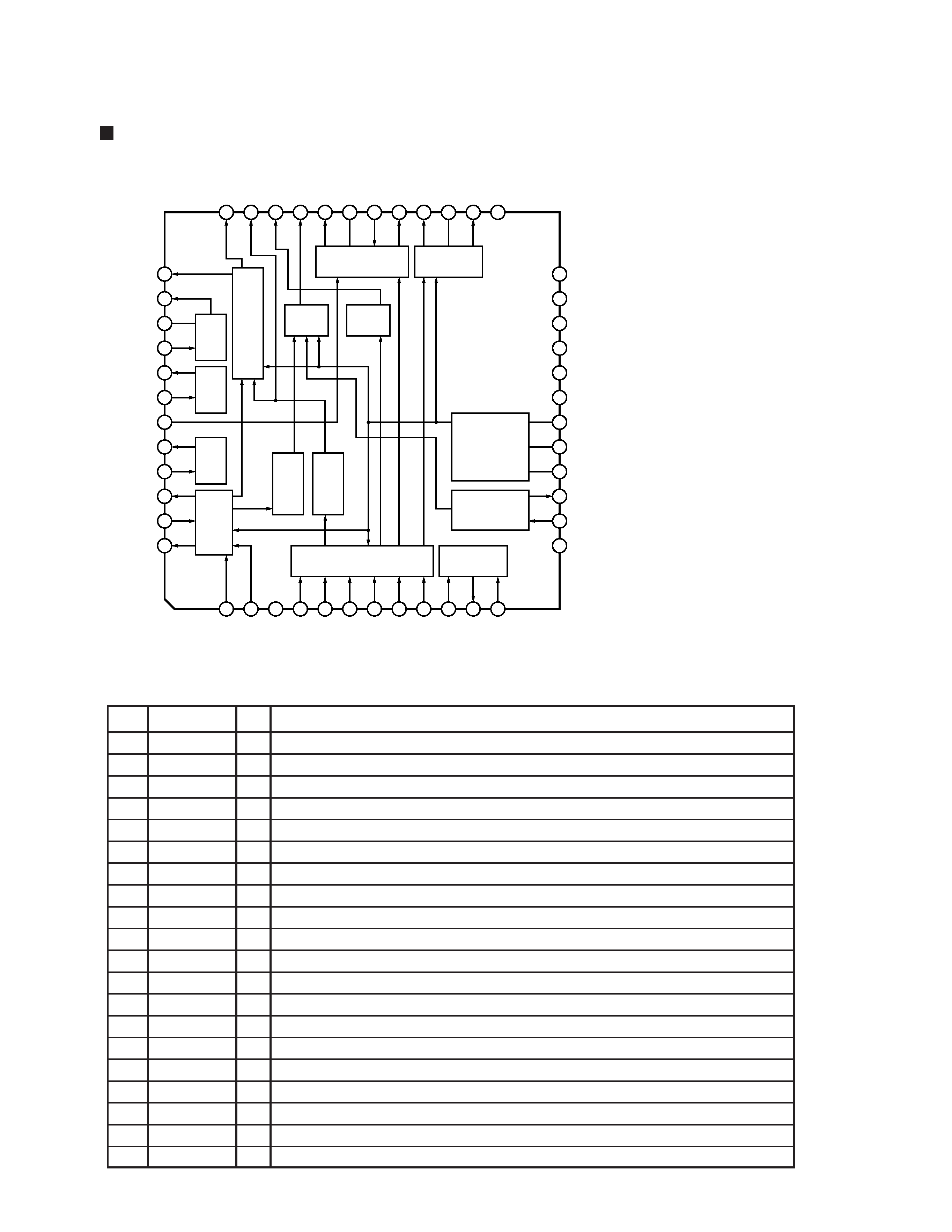
CXA2523AR(IC310):MD RF & Servo
1.Block Diagram
2.Pin Function
1
2
3
4
5
6
7
8
9
10
11
12
13
14
15
16
17
18
19
20
I-V converted RF signal I input.
I-V converted RF signal J input.
Vcc/2 voltage output.
A current input for main beam servo signal.
B current input for main beam servo signal.
C current input for main beam servo signal.
D current input for main beam servo signal.
E current input for side beam servo signal.
F current input for side beam servo signal.
Reflection light quantity monitor signal input.
Laser APC output.
Reference voltage input for the laser power intensity setting.
Connect to GND.
Connects the temperature sensor.
Connects the temperature sensor. outputs the reference voltage.
Data input for microcomputer serial interface.
Shift clock input for microcomputer serial interface.
Latch signal input for microcomputer serial interface.Latched when low.
Standby setting pin. Normal operation when high Standby when low.
Internal current source setting pin.
I
J
VC
A
B
C
D
E
F
PD
APC
APCREF
GND
TEMPI
TEMP R
SWDT
SCLK
XLAT
XSTBY
F0CNT
I
I
O
I
I
I
I
I
I
I
O
I
-
I
I
I
I
I
I
I
Pin No.
Symbol
I/O
Function
Description of Major ICs

XM-P55
XM-PJ1
2-2
21
22
23
24
25
26
27
28
29
30
31
32
33
34
35
36
37
38
39
40
41
42
43
44
45
46
47
48
Reference voltage output.
Equalizer center frequency setting pin.
BPF3T center frequency setting pin.
Power supply.
BPF22 center frequency setting pin.
Tracking error signal output.
Connects the sled error signal LPF capacitor.
Sled error signal output.
ADIP FM signal output.
ADIP signal comparator input.
Connects the ADIPAGC capacitor.
ADIP2 binary value signal output.
13 output / temperature signal output. Switched with serial commands.
Focus error signal output.
Reflection light quantity signal output for the main beam servo detector.
RF/ABCD bottom hold signal output.
Peak hold signal output for the RF/ABCD signals.
RF equalizer output.
Connects the RFAGC capacitor.
RFAGC input.
User comparator output.
User comparator non-inverted input.
Connects the capacitor for ADIP amplifier feedback circuit.
User operational amplifier output.
User operational amplifier inverted input.
RF amplifier output. Eye pattern checkpoint.
Input of the groove RF signal with AC coupling.
Groove RF signal output.
VREF
EQADJ
3TADJ
Vcc
WBLADJ
TE
CSLED
SE
ADFM
ADIN
ADAGC
ADFG
AUX
FE
ABCD
BOTM
PEAK
RF
RFAGC
AGCI
COMPO
COMPP
ADDC
OPO
OPN
RFO
MORFI
MORFO
O
I/O
I/O
-
I/O
O
-
O
O
I
-
O
O
O
O
O
O
O
-
I
O
I
I/O
O
I
O
I
O
Pin No.
Symbol
I/O
Function
XM-P55
XM-PJ1
2-3
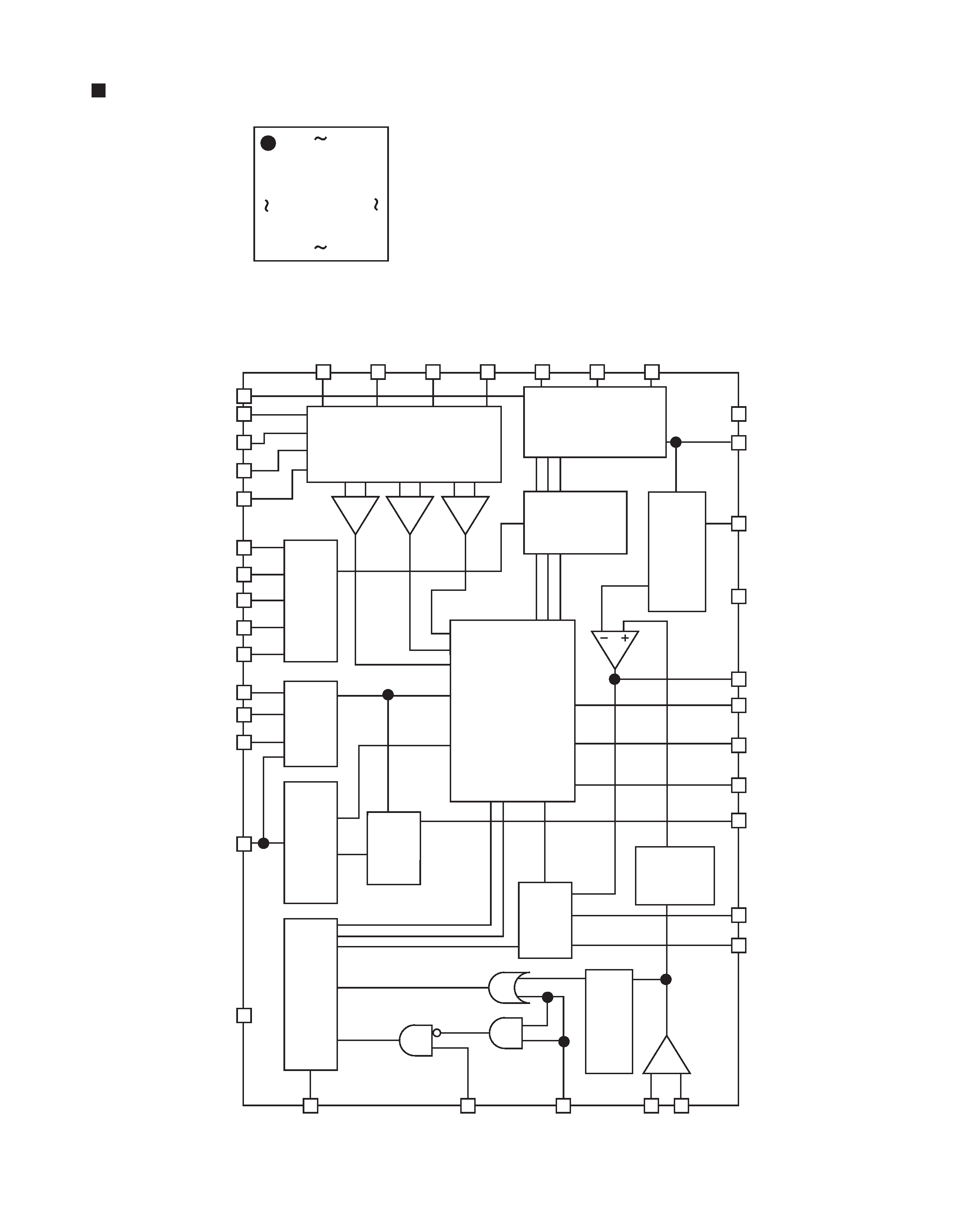
CXA8069M(IC450):Sensorless Motor Driver
48
37
13
24
12
1
25
36
UIN
VIN
WIN
COM
UOUT
VOUT
WOUT
PGND
RF
CF
GND
FC
FG2
FG
RESET
CLOCK
SLOPE
OSC
VS
WF
VF
UF
COMF
CPOUT
CPC2
CP2
CPC1
CP1
VCO
RMAX
RMIN
VCOIN
VCC
MCLOCK
S/S
BRAKE
VCONT
VCREF
+ -
+ -
+ -
+ -
Voltage Driver
Power Stage
Level Shifter
Charge
Pump
VCO
Sensorless
Logic
Phase
Comparator
1/8
Timing
Controllor
PWM
F/R
Controllor
Full Wave
Rectifier
Sample
and
Hold
1.Pin Layout
2.Block Diagram