COPYRIGHT © 2002 VICTOR COMPANY OF JAPAN, LTD
This service manual is printed on 100% recycled paper.
SERVICE MANUAL
Camera head section
L
Image sensing device
: 1/3-inch PS-CCD (350,000 pixels)
L
Shooting system
: 3-CCD system
L
Color separation optical system : 1/3-inch F1.4 3-color separation prism
L
Number of effective pixels
: 659 (horizontal) x 494 (vertical), 330,000 pixels approximately
L
Camera output
: 19 pins
L
Lens mount
: Standard C mount ( flange back: 17.526 mm in air)
L
Dimensions
: Camera head; 44 (W) x 51.4 (H) x 57.7 (D) mm (1-6/8" x 2-1/16" x 2-2/8") (not including
protrusion and camera cable etc)
L
Weight
: Camera head; 100 g (0.22 lbs.)
L
Classification
: Type CF applied part
Camera control unit section
L
Number of scanning lines
: 1125 (980 effective)
L
Scanning system
: 2:1 interlace (HD output, NTSC output)
Progressive (SXGA output)
L
Scanning frequency
: HD OUT 33.71625kHz (horizontal), 59.94 Hz (vertical)
SXGA OUT 67.4325kHz(horizontal), 59.94 Hz (vertical)
NTSC OUT 15.73425kHz(horizontal), 59.94 Hz (vertical)
L
Aspect ratio
: 4:3
L
Horizontal resolution (center)
: 750 TV lines TYP. (HD Y output, SXGA output)
L
Vertical resolution (center)
: 700 TV lines TYP. (HD Y output, SXGA output)
L
S/N
: 52dB
L
Sensitivity
: F6.8, 2000 lx
L
Minimum subject illuminance
: 5 lx
L
Sync system
: Internal sync/external sync
L
External sync signal input
: Composite sync signal of
±0.3 Vp-p, 75 ohms, BNC x 1 (ITU-R Rec.BT .709-3 HDTV standard
compliant)
L
Color bar
: Full color bar
L
Contour correction
: Horizontal dual-edged (7-step variable)
Vertical dual-edged (7-step variable)
L
Electronic shutter speed
: 1/60 s (normal), 1/100 s, 1/175 s, 1/250 s, 1/375 s, 1/500 s, 1/1000 s, 1/2000 s,1/4000s,
1/10000s
L
Video output
· SXGA signal
: R/G/B 0.7 Vp-p, 75 ohms HD/VD TTL
D-Sub mini 15 pin
· HD signal
: Y 1 Vp-p Pb/Pr 0.7 Vp-p 75 ohms BNC x 3
· NTSC signal
: VBS 1 Vp-p 75 ohms BNC Y/C 1 Vp-p 75 ohms S terminal
· DV signal
: IEEE1394 6 pins
L
Camera input
: 19 pins
L
Date indication
: Menu system 1) Year, month, day 2) Day, month, year 3) Month, day, year
L
Time indication
: Menu system, hour : minute: second
L
Rating
: 120V AC 60Hz, 0.7A
L
Classification of insulation : Class I
L
Operating environment
:+5
°C to +35°C (41°F to 95°F), 35 75%
L
Storage environment
: -20
°C to +50°C (-4°F to 102°F), 35 80%
L
Dimensions
: 280 (W) x 140 (H) x 300 (D) mm
(11-3/16" x 5-9/16" x 11-13/16") (excluding the protrusion and switches etc)
L
Weight
: 5.5 kg (12.1 lbs.)
L
Accessories
: Power cord x 1
Instruction manual x 1
Warranty card x 1
No.86711
2002/12
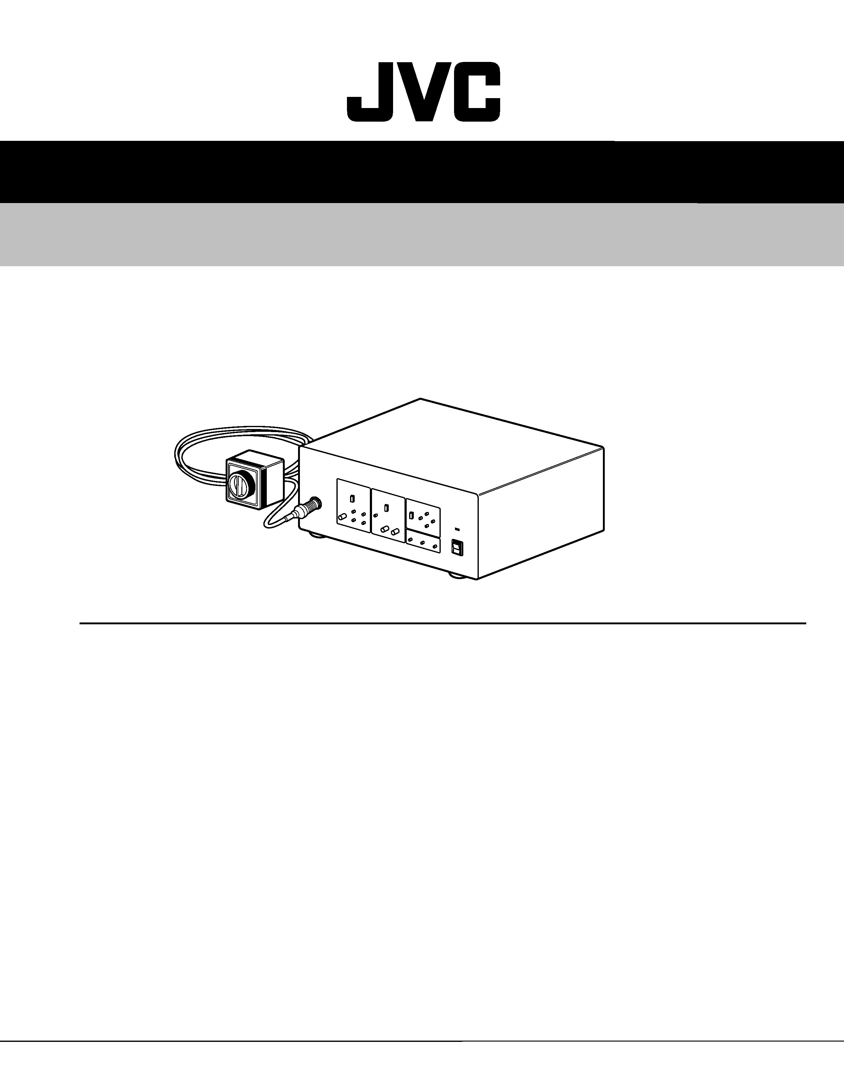
DZ-VCA3U
DZ-VCA3U S14H42
MICRO HD CAMERA
SPECIFICATIONS

1
TABLE OF CONTENTS
Section
Title
Page
Section
Title
Page
Important Safety Precautions
INSTRUCTIONS
1. PRECAUTIONS OF SERVICING
1.1 BEFORE DISASSEMBLING AND REASSEMBLING ... 1-1
1.1.1 Precautions ........................................................... 1-1
1.1.2 Disassembly of optical block assembly .................. 1-1
1.2 PREPARATION AND PRELIMINARY CHECK
REQUIRED FOR ADJUSTMENT ............................. 1-1
1.2.1 Before adjustment ................................................. 1-1
1.2.2 Tools and jigs required for repair and adjustment ... 1-1
1.3 Standard setup ............................................................ 1-2
1.4 How to set the "ADJUSTNENT MODE" ...................... 1-2
1.5 How to set the "DEBUG MODE" ................................. 1-2
1.6 How to do "ALL RESET" ............................................. 1-2
Warnings for accident prevention in handking battery ....... 1-3
1.7 SERVICE CAUTIONS ................................................. 1-4
1.7.1 Precautions ........................................................... 1-4
1.7.2 How to read the disassembly and assembly ......... 1-4
1.7.3 Connection of the wires ........................................ 1-4
1.7.4 Disassembly procedure ......................................... 1-5
1.8 WIRING AND BOARD LAYOUT .................................. 1-8
2. ELECTRICAL ADJUSTMENT
2.1 INITIAL SETTING ....................................................... 2-1
2.1.1 Functions and initial settings of
internal switches of boards ................................. 2-1
2.1.2 Adjustment procedure ........................................... 2-2
2.2 MTP BOARD ADJUSTMENT ...................................... 2-3
2.2.1 Adjustment part(s) location guide ........................... 2-3
2.2.2 Input voltage check ............................................... 2-3
2.2.3 output voltage level ................................................ 2-3
2.2.4 output voltage check(1) .......................................... 2-3
2.2.5 output voltage check(2) .......................................... 2-3
2.2.6 output voltage check(3) .......................................... 2-3
2.3 MICOM BOARD ADJUSTMENT .................................. 2-4
2.3.1 Adjustment part(s) location guide ........................... 2-4
2.3.2 Main clock level ...................................................... 2-4
2.3.3 GENLOCK output level .......................................... 2-4
2.4 DSP BOARD ADJUSTMENT ....................................... 2-5
2.4.1 Adjustment part(s) location guide ........................... 2-5
2.4.2 HD OUT ................................................................. 2-5
2.4.2.1 Y signal ratio level ............................................. 2-5
2.4.2.2 Y signal level ..................................................... 2-5
2.4.2.3 Pr signal raio level ............................................. 2-6
2.4.2.4 Pr signal level .................................................... 2-6
2.4.2.5 Pb signal ratio level ........................................... 2-6
2.4.2.6 Pb signal level ................................................... 2-6
2.4.3 SXGA OUT ............................................................. 2-7
2.4.3.1 G gain level ....................................................... 2-7
2.4.3.2 B gain level ....................................................... 2-7
2.4.3.3 R gain level ....................................................... 2-7
2.5 NTSC BOARD ADJUSTMENT .................................... 2-8
2.5.1 Adjustment part(s) locatio guide ............................. 2-8
2.5.2 INPUT SIGNAL ...................................................... 2-8
2.5.2.1 G gain level ....................................................... 2-8
2.5.2.2 B gain level ....................................................... 2-8
2.5.2.3 R gain level ....................................................... 2-9
2.5.3 OUTPUT SIGNAL .................................................. 2-9
2.5.3.1 Video level (1) ................................................... 2-9
2.5.3.2 Video level (2) ................................................... 2-9
2.5.3.3 Y level ............................................................... 2-9
2.5.3.4 Color level ....................................................... 2-10
2.5.3.5 DV signal check .............................................. 2-10
2.6 AD BOARD ASJUSTMENT ........................................ 2-11
2.6.1 Adjustment part(s) location guide ......................... 2-11
2.6.2 A/D AND AUTO GAIN .......................................... 2-11
2.6.2.1 A/D gain level .................................................. 2-11
2.6.2.2 AUTO gain level .............................................. 2-11
2.6.2.3 Color gain ........................................................ 2-12
2.6.2.4 Color gain for tint adjustment .......................... 2-12
2.6.2.5 White defect .................................................... 2-12
3. INSTALLATION MANUAL
1. Precautions .................................................................... 3-1
2. Connection of system components ................................ 3-1
3. Connection of each unit to the power supply unit .......... 3-1
4. Check of grounding (AA-V31U) ..................................... 3-2
5. Check of operation ......................................................... 3-2
6. Liaison slip of customer data ......................................... 3-2
7. Sterilization .................................................................... 3-2
8. Report of complaints dealt with ...................................... 3-2
4. CHARTS AND DIAGRAMS
4.1 BOARD INTERCONNECTIONS ................................. 4-3
4.2 MTP SCHEMATIC DIAGRAM ...................................... 4-5
4.3 AD IO SCHEMATIC DIAGRAM .................................... 4-7
4.4 ANALOG SCHEMATIC DIAGRAM ............................... 4-9
4.5 ADC SCHEMATIC DIAGRAM .................................... 4-11
4.6 SSG1 SCHEMATIC DIAGRAM .................................. 4-13
4.7 F MEN SCHEMATIC DIAGRAM ................................ 4-15
4.8 FLASH SCHEMATIC DIAGRAM ................................ 4-17
4.9 AMDP IO SCHEMATIC DIAGRAM ............................ 4-19
4.10 AMDP G SCHEMATIC DIAGRAM ........................... 4-21
4.11 AMDP B SCHEMATIC DIAGRAM ............................ 4-23
4.12 AMDP R SCHEMATIC DIAGRAM ............................ 4-25
4.13 AMDP FM SCHEMATIC DIAGRAM ......................... 4-27
4.14 AMDP 01 SCHEMATIC DIAGRAM .......................... 4-29
4.15 DSP-1 SCHEMATIC DIAGRAM ............................... 4-31
4.16 DSP-2 SCHEMATIC DIAGRAM ............................... 4-33
4.17 DSP-3 SCHEMATIC DIAGRAM ............................... 4-35
4.18 MICOM SCHEMATIC DIAGRAM ............................. 4-37
4.19 MICOM2 SCHEMATIC DIAGRAM ........................... 4-39
4.20 MICOM3 SCHEMATIC DIAGRAM ........................... 4-41
4.21 MICOM4 SCHEMATIC DIAGRAM ........................... 4-43
4.22 NTSC-2 SCHEMATIC DIAGRAM ............................ 4-45
4.23 NTSC-1 SCHEMATIC DIAGRAM ............................ 4-47
4.24 NTSC-5 SCHEMATIC DIAGRAM ............................ 4-48
4.25 NTSC-3 SCHEMATIC DIAGRAM ............................ 4-49
4.26 NTSC-4 SCHEMATIC DIAGRAM ............................ 4-51
4.27 NTSC-6 SCHEMATIC DIAGRAM ............................ 4-53
4.28 DV-1 SCHEMATIC DIAGRAM ................................. 4-55
4.29 DV-2 SCHEMATIC DIAGRAM ................................. 4-57
4.30 DV-3 SCHEMATIC DIAGRAM ................................. 4-59
4.31 FRT/LED SCHEMATIC DIAGRAM .......................... 4-61
4.32 MTP CIRCUIT BOARD ............................................ 4-63
4.33 AD CIRCUIT BOARD ............................................... 4-67
4.34 AMDP CIRCUIT BOARD .......................................... 4-71
4.35 DSP CIRCUIT BOARD ............................................ 4-75
4.36 MICOM CIRCUIT BOARD ....................................... 4-79
4.37 NTSC CIRCUIT BOARD .......................................... 4-83
4.38 DV CIRCUIT BOARD ............................................... 4-87
4.39 FRT & LED CIRCUIT BOARDS ............................... 4-89
4.40 CAMERA SYSTEM BLOCK DIAGRAM ................... 4-91
5. PARTS LIST
5.1 PACKING AND ACCESSORY ASSEMBLY<M1> ....... 5-1
5.2 CAMERA CONTROL UNIT ASSEMBLY<M3> ............ 5-2
5.3 ELECTRICAL PARTS LIST ......................................... 5-5
MTP BOARD ASSEMBLY<01> ........................................ 5-5
AD BOARD ASSEMBLY<02> .......................................... 5-6
AMDP BOARD ASSEMBLY<03> ................................... 5-11
DSP BOARD ASSEMBLY<04> ...................................... 5-15
MICOM BOARD ASSEMBLY<05> ................................. 5-18
NTSC BOARD ASSEMBLY<06> ................................... 5-21
DV BOARD ASSEMBLY<07> ........................................ 5-25
FRT BOARD ASSEMBLY<08> ...................................... 5-26
LED BOARD ASSEMBLY<09> ...................................... 5-27
Important Safety Precautions
Prior to shipment from the factory, JVC products are strictly inspected to conform with the recognized product safety and electrical codes
of the countries in which they are to be sold. However, in order to maintain such compliance, it is equally important to implement the
following precautions when a set is being serviced.
Fig.1
1. Locations requiring special caution are denoted by labels and
inscriptions on the cabinet, chassis and certain parts of the
product. When performing service, be sure to read and com-
ply with these and other cautionary notices appearing in the
operation and service manuals.
2. Parts identified by the
symbol and shaded (
) parts
such as fuses and circuit protectors are critical for safety.
Replace only with specified part numbers.
3. Fuse replacement caution notice.
Caution for continued protection against fire hazard.
Replace only with same type and rated fuse(s) as specified.
4. Use specified internal wiring. Note especially:
1) Wires covered with PVC tubing
2) Double insulated wires
3) High voltage leads
5. Use specified insulating materials for hazardous live parts.
Note especially:
1) Insulation Tape
3) Spacers
5) Barrier
2) PVC tubing
4) Insulation sheets for transistors
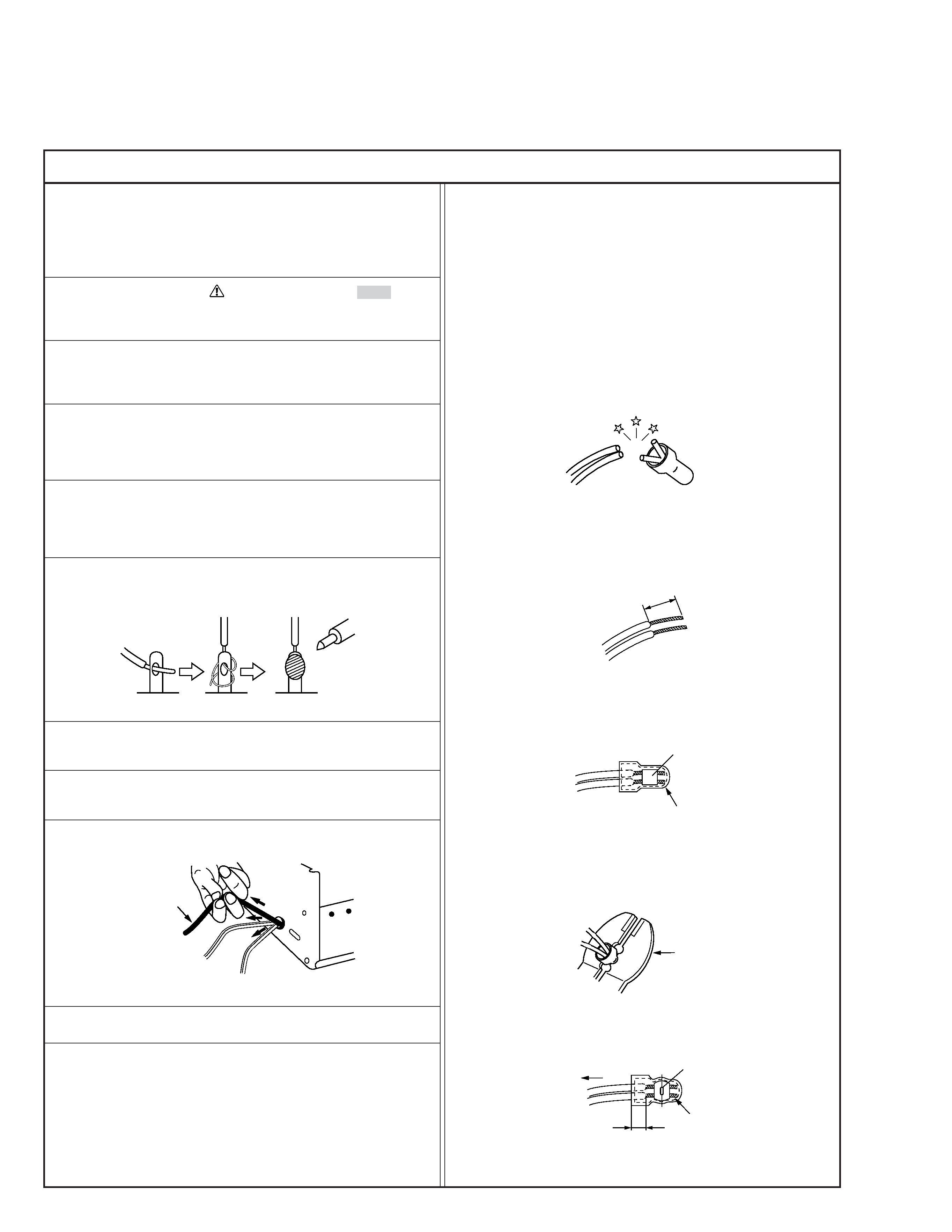
6. When replacing AC primary side components (transformers,
power cords, noise blocking capacitors, etc.) wrap ends of
wires securely about the terminals before soldering.
Power cord
Fig.2
10. Also check areas surrounding repaired locations.
11. Products using cathode ray tubes (CRTs)
In regard to such products, the cathode ray tubes themselves,
the high voltage circuits, and related circuits are specified for
compliance with recognized codes pertaining to X-ray emission.
Consequently, when servicing these products, replace the cath-
ode ray tubes and other parts with only the specified parts.
Under no circumstances attempt to modify these circuits.
Unauthorized modification can increase the high voltage value
and cause X-ray emission from the cathode ray tube.
12. Crimp type wire connector
In such cases as when replacing the power transformer in sets
where the connections between the power cord and power
transformer primary lead wires are performed using crimp type
connectors, if replacing the connectors is unavoidable, in or-
der to prevent safety hazards, perform carefully and precisely
according to the following steps.
1) Connector part number : E03830-001
2) Required tool : Connector crimping tool of the proper type
which will not damage insulated parts.
3) Replacement procedure
(1) Remove the old connector by cutting the wires at a point
close to the connector.
Important : Do not reuse a connector (discard it).
Fig.7
cut close to connector
Fig.3
(2) Strip about 15 mm of the insulation from the ends of
the wires. If the wires are stranded, twist the strands to
avoid frayed conductors.
15 mm
Fig.4
(3) Align the lengths of the wires to be connected. Insert
the wires fully into the connector.
Connector
Metal sleeve
Fig.5
(4) As shown in Fig.6, use the crimping tool to crimp the
metal sleeve at the center position. Be sure to crimp fully
to the complete closure of the tool.
1
Precautions during Servicing
7. Observe that wires do not contact heat producing parts
(heatsinks, oxide metal film resistors, fusible resistors, etc.)
8. Check that replaced wires do not contact sharp edged or
pointed parts.
9. When a power cord has been replaced, check that 10-15 kg of
force in any direction will not loosen it.
1.25
2.0
5.5
Crimping tool
Fig.6
(5) Check the four points noted in Fig.7.
Not easily pulled free
Crimped at approx. center
of metal sleeve
Conductors extended
Wire insulation recessed
more than 4 mm
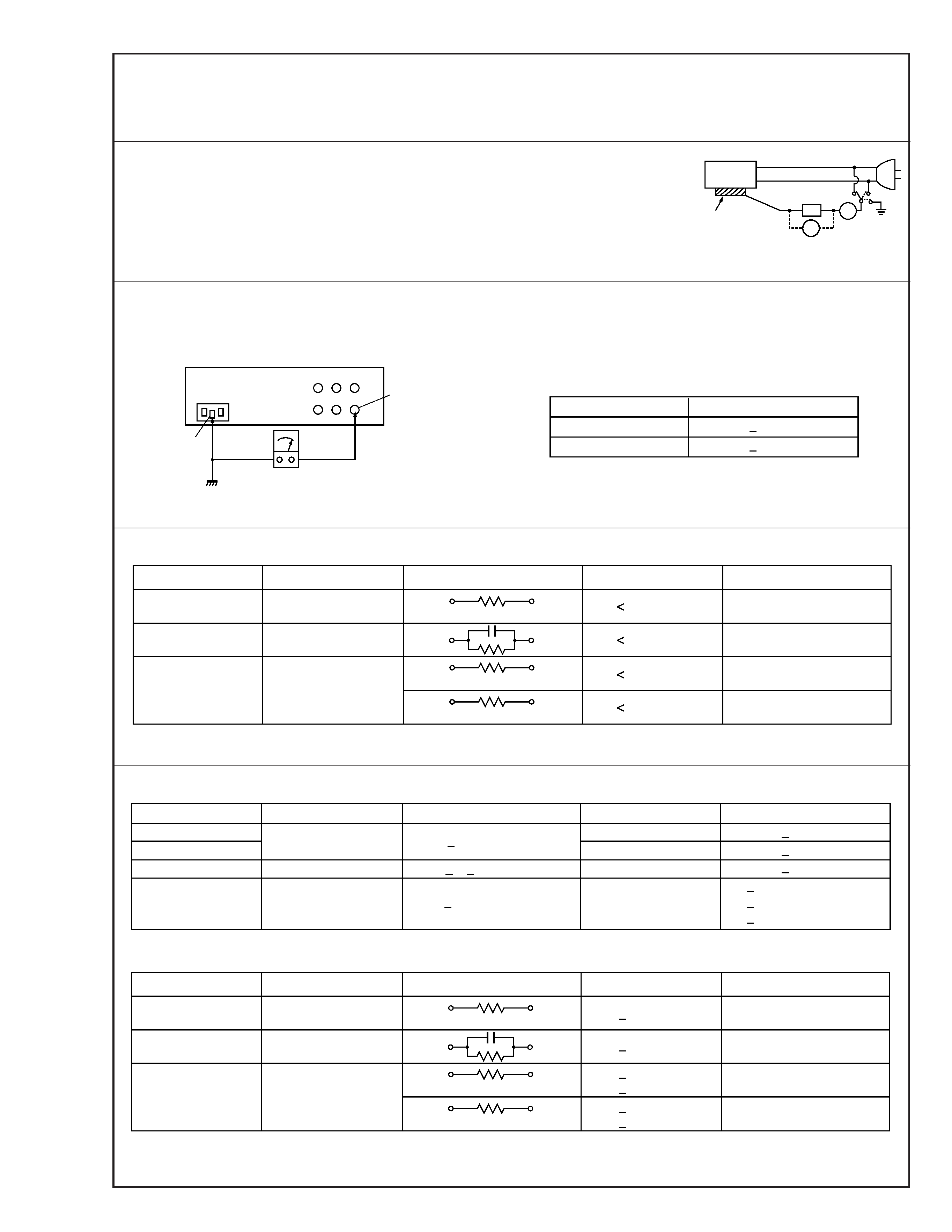
Safety Check after Servicing
Examine the area surrounding the repaired location for damage or deterioration. Observe that screws, parts and wires have been
returned to original positions, Afterwards, perform the following tests and confirm the specified values in order to verify compli-
ance with safety standards.
1. Leakage current test
Confirm specified or lower leakage current between earth ground/power cord plug prongs
and externally exposed accessible parts (RF terminals, antenna terminals, video and audio
input and output terminals, microphone jacks, earphone jacks, etc.).
Measuring Method : (Power ON)
Insert load Z between earth ground/power cord plug prongs and externally exposed accessi-
ble parts. Use an AC voltmeter to measure across both terminals of load Z. See figure 9 and
following table 2.
2. Grounding (Class 1 model only)
Confirm specified or lower grounding impedance between earth pin and externally exposed accessible parts (Video in, Video out,
Audio in, Audio out or Fixing screw etc.).
Measuring Method:
Connect milli ohm meter between earth pin and exposed accessible parts. See figure 10 and grounding specifications.
Region
USA & Canada
Europe & Australia
Grounding Impedance (Z)
Z
0.2 ohm
Z
0.2 ohm
Earth pin
Earth
Exposed accessible part
Milli ohm meter
Grounding Specifications
Fig. 9
ab
c
V
A
Externally
exposed
accessible part
Z
Fig. 8
Clearance Distance (d), (d')
d, d'
3 mm
d, d'
4 mm
d, d'
3.2 mm
1 MØ
R
12 MØ/500 V DC
Dielectric Strength
AC 1 kV 1 minute
AC 1.5 kV 1 miute
AC 1 kV 1 minute
AC Line Voltage
100 V
100 to 240 V
110 to 130 V
110 to 130 V
200 to 240 V
Japan
USA & Canada
Europe & Australia
R
10 MØ/500 V DC
Region
Insulation Resistance (R)
R
1 MØ/500 V DC
AC 3 kV 1 minute
(Class
2)
AC 1.5 kV 1 minute
(Class
1)
d
4 mm
d'
8 mm (Power cord)
d'
6 mm (Primary wire)
Table 2 Specifications for each region
a, b, c
Leakage Current ( i )
AC Line Voltage
110 to 130 V
220 to 240 V
Japan
USA & Canada
i
1 mA rms
Exposed accessible parts
Exposed accessible parts
Antenna earth terminals
Other terminals
i
0.5 mA rms
i
0.7 mA peak
i
2 mA dc
i
0.7 mA peak
i
2 mA dc
Europe & Australia
Region
Load Z
1 kØ
2 kØ
1.5 kØ
0.15
µF
50 kØ
100 V
110 to 130 V
Table 3 Leakage current specifications for each region
Note: These tables are unofficial and for reference only. Be sure to confirm the precise values for your particular country and locality.
2
< GENERAL USE >
a, b, c
Leakage Current ( i )
AC Line Voltage
110 to 130 V
220 to 240 V
Japan
USA & Canada
Exposed accessible parts
Exposed accessible parts
Antenna earth terminals
Other terminals
Europe & Australia
Region
Load Z
1 kØ
2 kØ
1.5 kØ
0.15
µF
50 kØ
100 V
110 to 130 V
i
0.1 mA
i
0.1 mA
i
0.1 mA
i
0.1 mA
Table 1 Leakage current specifications for each region
< MEDICAL USE >
1-1
SECTION 1
PRECAUTIONS FOR SERVICING
1.1 BEFORE DISASSEMBLING AND REASSEMBLING
1.1.1
Precautions
1. When disconnecting and reconnecting connectors, pay care-
ful attention to their wirings not to damage them, particularly
to the wiring of the CCU's camera connector that requires
the most meticulous care for disconnection and connection.
2. When unsoldering chip parts (IC in particular) for replace-
ment, completely remove solder particles from them and their
surroundings beforehand. Moreover, pay heed to the circuit
pattern not to exfoliate it from the substrate during replace-
ment of a chip part.
3. Don't use any chip part that was once removed.
4. Handle the optical block assembly with meticulous care.
Don't apply it a strong shock.
5. There is a lithium battery for backing up the timer on the
POWER board assembly. Pay careful attention to the lithium
battery for accident prevention.
1.1.2
Disassembly of optical block assembly
Since the CCD is precisely glued to the prism in the optical
block assembly, the CCD cannot be replaced individually if
it comes into failure. Therefore, the optical block assembly
is subject to repair by the JVC Home AV Network Business
Unit. If there is something wrong in the optical block assem-
bly, send the camera head assembly whole with a written
request filled out with necessary matters to the Service En-
gineering Section, Home AV Network Business Unit, JVC.
1.2 PREPARATION AND PRELIMINARY CHECK
REQUIRED FOR ADJUSTMENT
1.2.1
Before adjustment
1. Use two or more lighting apparatuses whose color tempera-
ture is 3200K for illuminating the test pattern, and uniformly
light up the test pattern surface with illuminance of 4000 lx
approximately while checking it with an illuminometer. If the
pattern surface is unevenly illuminated, adjustment may re-
sult in failure. Carefully set up lighting apparatuses so that
the test pattern is illuminated uniformly. (It is desired to use
two or more light sources.)
2. Be sure to use a clean test pattern as far as circumstances
permit.
1.2.2
Tools and jigs required for repair and adjustment
Use the following tools, jigs and test instruments to perform
check and adjustment properly.
1) Multiscan monitor and color monitor
For SXGA(G, B,R) signal : Flex Scan T962 (or equal)
For HD(Y,PB,PR) signal : DT-V1900CG(U) (or equal)
For NTSC siganl
: DT-V1900CG(U) (or equal)
2) 1/2" professional zoom lens (Model No. YH13x7.5B12 or
YH13x7.5K12 is recommended by the Professional Video
Division)
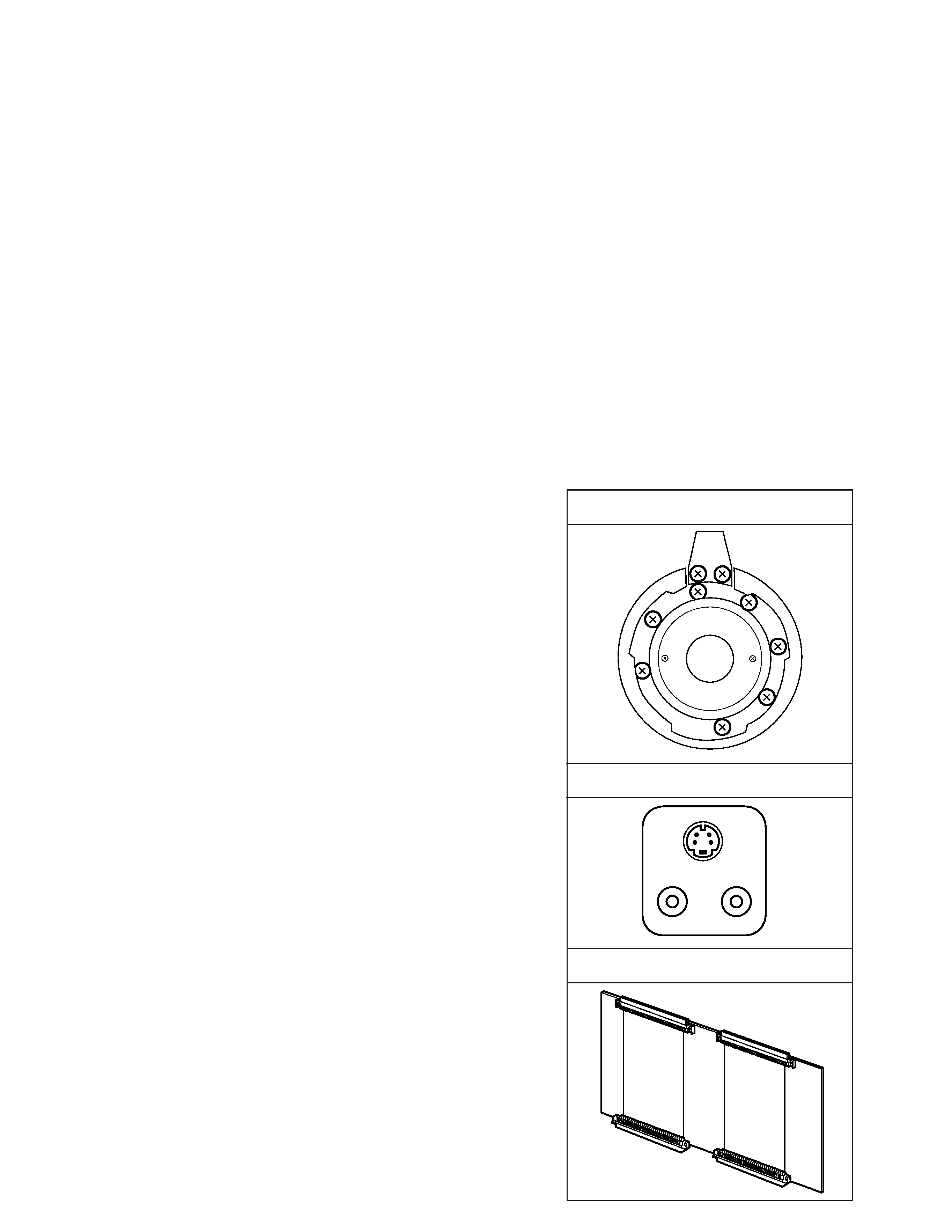
3) C mount adapter (Model No. ACM-11)
4) Tripod
5) RCA cable
6) SXGA cable
7) Extension board
8) Resolution chart for HDTV
9) Gray scale chart (for NTSC, Part No. GS-2A)
10) Oscilloscope (for 300 MHz or more)
11) Wrench for removing connector ring
12) Illuminometer
13) Color temperature meter
14) Digital voltmeter
15) Lighting apparatus (3200 K halogen lamp)
C mount adapter (ACM-11)
RCA - S Adapter (PTU93001A)
Extension board