- 1 -
EN-1187B
Published by Service Dept.
Printed in Japan
Clarion Co., Ltd.
50 Kamitoda, Toda-shi, Saitama 335-8511 Japan
Service Dept.: 5-66 Azuma , Kitamoto-shi, Saitama 364-0007 Japan
Tel: +81-48-541-2335 / 2432 FAX: +81-48-541-2703
298-6213-00 Jan.2005
Service Manual
Model
NISSAN Automobile Genuine
Satellite Tuner
EN-1187B
(Genuine No.28050 EH000)
SPECIFICATIONS
Receive range:
2332.5MHz to 2345.0MHz
Power supply voltage: 13.2V
(10.8 to 16.6V allowable)
Power consumption:
Less than 1A(with Antenna)
Antenna current limit:
0.2A
Dimensions(mm):
178(W) x 30(H) x 130(D)
Weight:
1110g
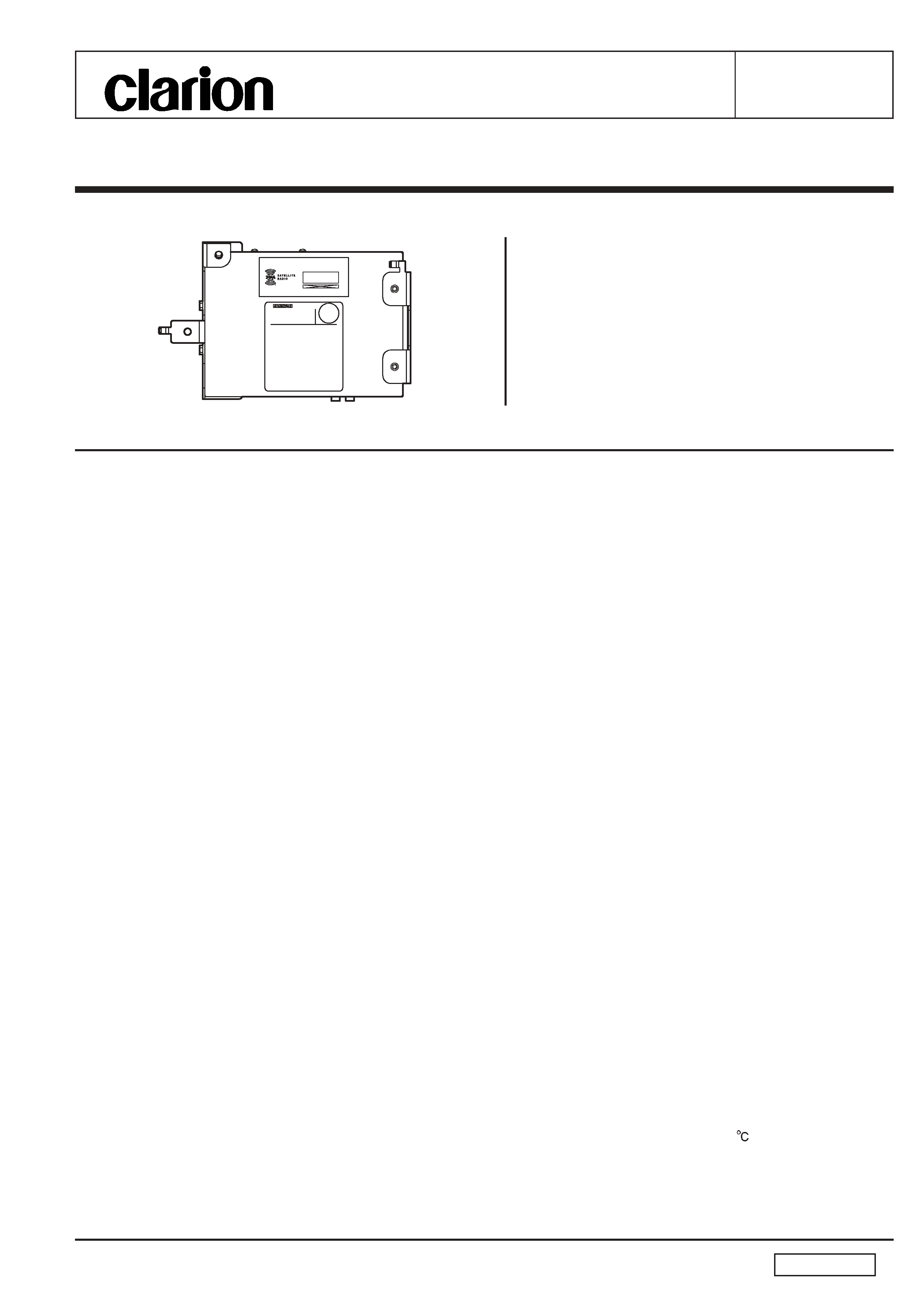
COMPONENTS
EN-1187B-A
Main unit
-----------
1
NOTES
*
Specifications and design are subject to change without
notice for further improvement.
*
We cannot supply PWB with component parts in prin-
ciple. When a circuit on PWB has failure, please repair
it by component parts base. Parts which are not men-
tioned in service manual are not supplied.
To engineers in charge of repair or
inspection of our products.
Before repair or inspection, make sure to follow the
instructions so that customers and Engineers in
charge of repair or inspection can avoid suffering
any risk or injury.
1. Use specified parts.
The system uses parts with special safety features against
fire and voltage. Use only parts with equivalent character-
istics when replacing them.
The use of unspecified parts shall be regarded as remod-
eling for which we shall not be liable. The onus of product
liability (PL) shall not be our responsibility in cases where
an accident or failure is as a result of unspecified parts
being used.
2. Place the parts and wiring back in their original positions
after replacement or re-wiring.
For proper circuit construction, use of insulation tubes,
bonding,gaps to PWB, etc, is involved. The wiring connec-
tion and routing to the PWB are specially planned using
clamps to keep away from heated and high voltage parts.
Ensure that they are placed back in their original positions
after repair or inspection.
If extended damage is caused due to negligence during
repair, the legal responsibility shall be with the repairing
company.
3. Check for safety after repair.
Check that the screws, parts and wires are put back se-
curely in their original position after repair. Ensure for safety
reasons there is no possibility of secondary ploblems
around the repaired spots.
If extended damage is caused due to negligence of repair,
the legal responsibility shall be with the repairing company.
4. Caution in removal and making wiring connection to the
parts for the automobile.
Disconnect the battery terminal after turning the ignition
key off. If wrong wiring connections are made with the bat-
tery connected, a short circuit and/or fire may occur. If ex-
tensive damage is caused due to negligence of repair, the
legal responsibility shall be with the repairing company.
5. Cautions regarding chips.
Do not reuse removed chips even when no abnormality is
observed in their appearance. Always replace them with
new ones. (The chip parts include resistors, capacitors,
diodes, transistors, etc). The negative pole of tantalum
capacitors is highly susceptible to heat, so use special care
when replacing them and check the operation afterwards.
6. Cautions in handling flexible PWB
Before working with a soldering iron, make sure that the
iron tip temperature is around 270 . Take care not to ap-
ply the iron tip repeatedly(more than three times)to the
same patterns. Also take care not to apply the tip with force.
7. Turn the unit OFF during disassembly and parts replace-
ment. Recheck all work before you apply power to the unit.
- 2 -
EN-1187B
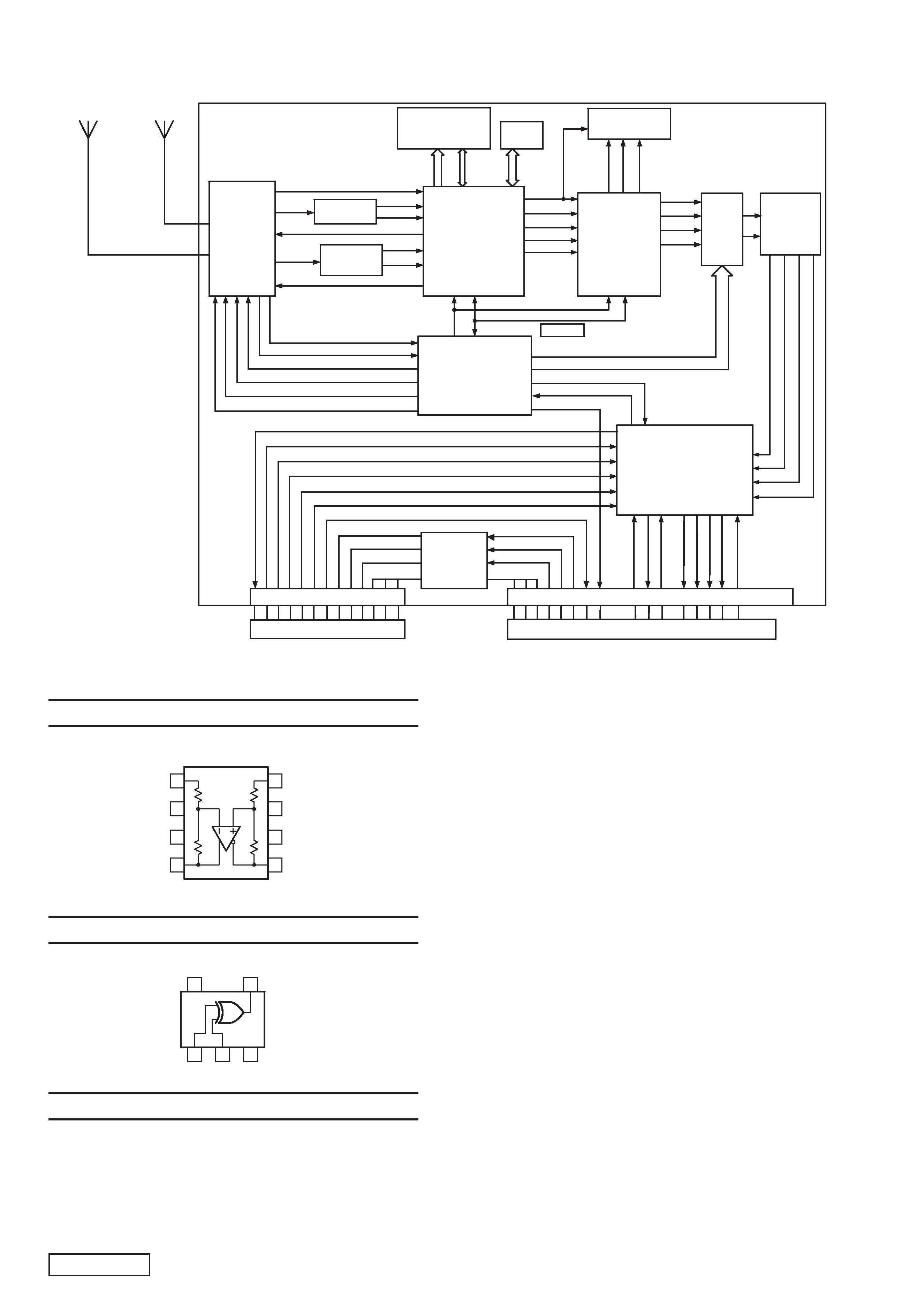
BLOCK DIAGRAM
XM TUNER
MODULE
(BL1)
STA400
Channel Decoder
(IC203)
STA450
Service/Source
Decoder
(IC205)
DAC
(IC502)
K4S280832E-TC75
SDRAM
(IC202)
AD8131
(IC101)
Ex.OR
(IC204)
Differential
Pre Amp
Block
M30624FGMFP
System controller
(IC307)
ST19AF08
(IC206)
C
o
n
tro
l
PCSD
PCDC
PCFS
MFP-PLL
M_CLK
MCLK
LRCLK
DATA
BCLK
R
L
Discrete
Circuit
TERR IF
SAT IF
IF Neg.
IF Pos.
IF Pos.
IF Neg.
SATELLITE
TERRESTRIAL
M_CLK_IN
SAT AGC
TERR AGC
M_RE
S
E
T
M_S
C
K
M_S
D
A
SCK
SDA
I2C-Bus
LOCK_DET
ANT_DET
DIV_SW
SPI_LE
SPI_CLK
Da
ta
SPI_DATA
Control
J602 TK-16 HW
J601 A-16 MW
CHG EXTENSION BLOCK
R
X
D
TXD
CONT
CNG-LCH(+)
C
NG-LC
H(-)
CNG-RCH(+)
CNG-R
C
H
(-)
REQ2
REQ1
RXD
TXD
S
O
URCE
CHA
N
GE
LCH(+)
LCH(-)
RCH(+)
RCH(-)
EX_CHG-LCH(+)
EX_CHG-LCH(-)
EX_CHG-RCH(+)
EX_CHG-RCH(-)
COMBI
AUTO-CHANGER
EX_RXD
EX_TXD
1
3
1
4
8
9
1
5
1
6
11
M
L
J
A
G
B
H
O
K
N
POWER
SUPPLY
BACK UP
ACC
ILLUMI
GND
D
F
E
I
C
P
2
6
1
0
1
1
2
4
BACK UP
ACC
ILLUMI
GND
EXPLANATION OF IC
051-4611-90
AD8131ARM
High-Speed Differential Driver
051-7278-08
SN74AHC1G86DCKR
Single Exclusive OR Gate
051-6391-00
STA450
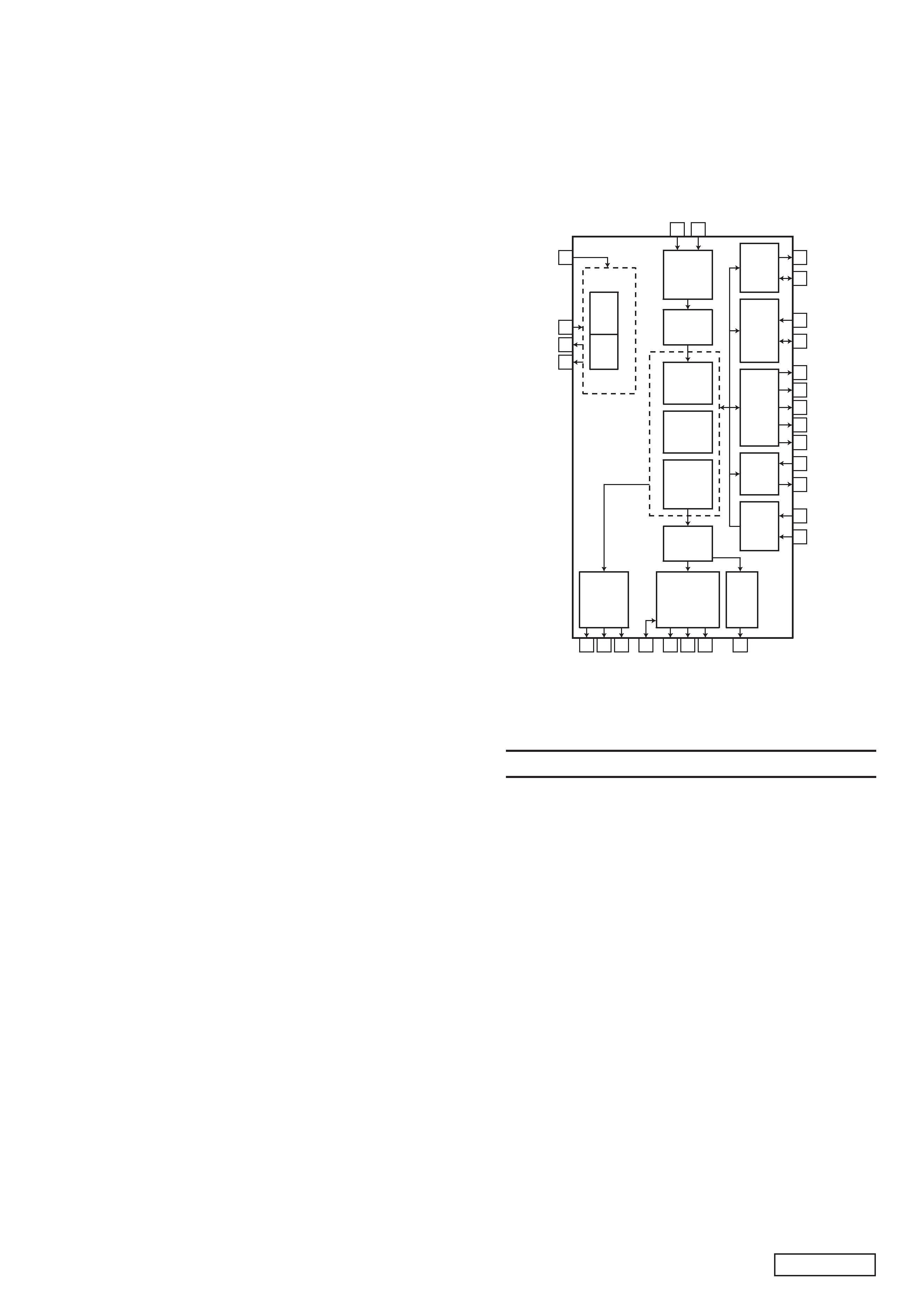
SERVICE LAYER & SOURCE DECODER
DESCRIPTION
The STA450 is designed for digital radio receivers, and integrates all
the functions needed to perform the Service Layer and Source Decod-
ing:
. Bitstream Synchronization
. Service Layer (SL) Demultiplexing
. Auxiliary Data Management
. Conditional Access (CA) Control
. Service Components Extraction
. Service Components Decryption
. Audio and Voice Decoding
The extracted Audio and Data are made available through different
interfaces:
. I2S Audio Output
. S/PDIF Output
. Data Port
Terminal Description
pin
1: NU
: IN : Not Used (must be connected to ground in
functional mode)
pin
2: GND
: - : Ground.
pin
3: VDD
: - : 2.5V Core Supply Voltage
pin
4: TEST 0
: IN : Test Pin (must be connected to ground in
functional mode)
pin
5: CLK IN
: IN : Clock Input
pin
6: NU
: IN : Not Used (must be connected to ground in
functional mode)
pin
7: TEST B
: IN : Test Pin
pin
8: CAP RST
: O : CAP Reset
pin
9: GND
: - : Ground.
pin 10: VDD
: - : 2.5V Core Supply Voltage
pin 11: VDD IO
: - : 3.3V I/O Supply Voltage
pin 12: CLK OUT
: O : Clock Out
pin 13: S CL M
: O : I2C Master Serial Clock
pin 14: S DA M
:I/O: I2C Master Serial Data
pin 15: GND
: - : Ground.
pin 16: VDD
: - : 2.5V Core Supply Voltage
pin 17: NU
: IN : Not Used (must be connected to ground in
functional mode)
pin 18: SCAN MODE
: IN : Scan Mode (must be connected to ground
in functional mode)
1
2
3
4
+Din
N.C.
V-
-Out
-Din
Vocm
V+
+Out
8
7
6
5
75
75
1.5k
1.5k
5
4
GND
VDD
1
2
3
- 3 -
EN-1187B
pin 19: A PLL GND
: - : Analog Ground for Audio PLL
pin 20: A PLL VDD
: - : 2.5V Analog Supply for Audio PLL
pin 21: FILT 0
: - : PLL Filter
pin 22: NU
: - : Not Used (must be terminated with the
same network as pin 21)
pin 23: GND
: - : Ground.
pin 24: VDD
: - : 2.5V Core Supply Voltage
pin 25: CLK M 1
: IN : Selection of Input Clock for the DSP core
and peripherals
pin 26: CLK M 0
: IN : Selection of Input Clock for the DSP core
and peripherals
pin 27: NU
: IN : Not Used (must be connected to ground in
functional mode)
pin 28: NU
: IN : Not Used (must be connected to ground in
functional mode)
pin 29: PLL SYNC
: IN : Fractional Audio PLL Sync.
pin 30: GND
: - : Ground.
pin 31: VDD
: - : 2.5V Core Supply Voltage
pin 32: VDD IO
: - : 3.3V I/O Supply Voltage
pin 33: PC DC
: IN : PC Bitstream Data Clock
pin 34: PC SD
: IN : PC Bitstream Serial Data
pin 35: NU
: IN : Not Used (must be connected to ground in
functional mode)
pin 36: NU
: O : Not used
pin 37: GND
: - : Ground.
pin 38: VDD
: - : 2.5V Core Supply Voltage
pin 39: PC FS
: IN : PC Bitstream PRC Frame Sync.
pin 40: NU
: IN : Not Used (must be connected to ground in
functional mode)
pin 41: NU
: IN : Not Used (must be connected to ground in
functional mode)
pin 42: NU
: IN : Not Used (must be connected to ground in
functional mode)
pin 43: NU
: IN : Not Used (must be connected to ground in
functional mode)
pin 44: GND
: - : Ground.
pin 45: VDD
: - : 2.5V Core Supply Voltage
pin 46: NU
: IN : Not Used (must be connected to ground in
functional mode)
pin 47: NU
: IN : Not Used (must be connected to ground in
functional mode)
pin 48: NU
: IN : Not Used (must be connected to ground in
functional mode)
pin 49: NU
: IN : Not Used (must be connected to ground in
functional mode)
pin 50: GND
: - : Ground.
pin 51: VDD
: - : 2.5V Core Supply Voltage
pin 52: VDD IO
: - : 3.3V I/O Supply Voltage
pin 53: NU
: IN : Not Used (must be connected to ground in
functional mode)
pin 54: TEST 1
: IN : Test Pin
pin 55: RESET N
: IN : HW Reset (active low)
pin 56: EVENT IRQ
: O : General Interrupt (Events, Errors, Data
ready)
pin 57: GND
: - : Ground.
pin 58: VDD
: - : 2.5V Core Supply Voltage
pin 59: S CL
: IN : I2C Slave Serial Clock
pin 60: S DA
:I/O: I2C Slave Serial Data
pin 61: INT 1
: O : Dedicated Errors Interrupt
pin 62: GND
: - : Ground.
pin 63: VDD
: - : 2.5V Core Supply Voltage
pin 64: INT 2
: O : Dedicated Errors Interrupt
pin 65: TEST
: O : Test Pin
pin 66: DP EN
: O : Data Port Enable
pin 67: DP DATA
: O : Data Port Data
pin 68: DP CLK
: O : Data Port Clock
pin 69: GND
: - : Ground.
pin 70: VDD
: - : 2.5V Core Supply Voltage
pin 71: VDD IO
: - : 3.3V I/O Supply Voltage
pin 72: LR CKT
: O : I2S Left & Right Clock
pin 73: S DO
: O : I2S Output Data (PCM Data)
pin 74: S CKT
: O : I2S Serial Clock
pin 75: O CLK
:I/O: Oversampling Clock
pin 76: GND
: - : Ground.
pin 77: VDD
: - : 2.5V Core Supply Voltage
pin 78: 1958 OUT
: O : S/PDIF Output
pin 79: RS232 TX
: O : RS232 Transmitter
pin 80: RS232 RX
: IN : RS232 Receiver (must be connected to
ground in functional mode)
PC
Bitstream
Input
Interface
34
33
PC
DC
PC
SD
Audio
Decoder
Output
Buf
fer
Audio
Port
Output
Interface
(PCM
I/F)
SPDIFF
Output
Data
port
Output
Interface
(USSIO
3)
1958
out
S
DO
S
CKT
LR
CKT
O
CLK
DP
CLK
DP
DA
T
A
DP
EN
DSP
BASED
Input
Buf
fer
Service
Layer
DeMUX
Decrypt
I2C
Master
(CAP
I/F)
I2C
Slave
(Syscon
I/F)
GPIO
Interface
RS232
External
Interrupt
S CL M
EVENT IRQ
S DA
S CL
S DA M
RS232 RX
CAP RST
TEST
INT 2
INT 1
PLL SYNC
PC FS
RS232 TX
8
65
64
61
56
79
80
29
39
59
60
14
13
78
74
72
73
75
67
68
66
21
System
&
Audio
Clocks
System
PLL
Audio
PLL
RESET N
CLK IN
FILT 0
CLK OUT
12
55
5
051-9327-00
K4S280832E-TC75
4M x 8bit x 4banks SDRAM
Terminal Description
pin
1: VDD
: - : Positive voltage supply.
pin
2: DQ 0
:I/O: The data input / output.
pin
3: VDD Q
: - : Positive power supply for the data I/O
ports.
pin
4: NU
: - : Not in use.
pin
5: DQ 1
:I/O: The data input / output.
pin
6: VSS Q
: - : Ground terminal for the data I/O ports.
pin
7: NU
: - : Not in use.
pin
8: DQ 2
:I/O: The data input / output.
pin
9: VDD Q
: - : Positive power supply for the data I/O
ports.
pin 10: NU
: - : Not in use.
pin 11: DQ 3
:I/O: The data input / output.
pin 12: VSS Q
: - : Ground terminal for the data I/O ports.
pin 13: NU
: - : Not in use.
pin 14: VDD
: - : Positive voltage supply.
pin 15: NU
: - : Not in use.
pin 16: WE
: IN : Write enable signal input.
pin 17: CAS
: IN : Column address strobe input.
pin 18: RAS
: IN : Raw address strobe input.
pin 19: CS IN
: IN : The chip select command input.
pin 20: BA 0
: IN : Bank address input.
pin 21: BA 1
: IN : Bank address input.
pin 22: A 10
: IN : Address signal input.
pin 23: A
0
: IN : Address signal input.
pin 24: A
1
: IN : Address signal input.

- 4 -
EN-1187B
pin 25: A
2
: IN : Address signal input.
pin 26: A
3
: IN : Address signal input.
pin 27: VDD
: - : Positive voltage supply.
pin 28: VSS
: - : Negative voltage supply.
pin 29: A
4
: IN : Address signal input.
pin 30: A
5
: IN : Address signal input.
pin 31: A
6
: IN : Address signal input.
pin 32: A
7
: IN : Address signal input.
pin 33: A
8
: IN : Address signal input.
pin 34: A
9
: IN : Address signal input.
pin 35: A 11
: IN : Address signal input.
pin 36: NU
: - : Not in use.
pin 37: CKE
: IN : Clock enable signal input.
pin 38: CLK
: IN : The clock pulse input.
pin 39: DQM
: IN : Makes data output Hi-Z, tSHZ after the
clock and masks the output. Blocks data
input when DQM active.
pin 40: NU
: - : Not in use.
pin 41: VSS
: - : Negative voltage supply.
pin 42: NU
: - : Not in use.
pin 43: VDD Q
: - : Positive power supply for the data I/O
ports.
pin 44: DQ 4
:I/O: The data input / output.
pin 45: NU
: - : Not in use.
pin 46: VSS Q
: - : Ground terminal for the data I/O ports.
pin 47: DQ 5
:I/O: The data input / output.
pin 48: NU
: - : Not in use.
pin 49: VDD Q
: - : Positive power supply for the data I/O
ports.
pin 50: DQ 6
:I/O: The data input / output.
pin 51: NU
: - : Not in use.
pin 52: VSS Q
: - : Ground terminal for the data I/O ports.
pin 53: DQ 7
:I/O: The data input / output.
pin 54: VSS
: - : Negative voltage supply.
051-6390-00
STA400
CHANNEL DECODER
DESCRIPTION
STA400 Channel Decoder integrates all the functions to demodulate and
decode the incoming satellite and terrestrial signals after the RF Front-
End down-convertion:
. Analog-to-Digital conversions
. Satellite and terrestrial demodulation
. AGC
. Frame synchronization and demultiplexing
. Viterbi decoding
. Time and spatial diversity combining
. Reed-Solomon decoding and deinterleaving
. Prime Rate Channel (PRC) demultiplexing
. Payload Channel (PC) selection
At the end of the demodulation and decoding processes a configurable
serial data stream is made available to STA450, the Service/Source
Decoder, via the PC Bitstream interface.
Terminal Description
pin
1: F TEST OUT 10: O : Configurable Functional Test Output
pin
2: F TEST OUT 11: O : Configurable Functional Test Output
pin
3: F TEST OUT 12: O : Configurable Functional Test Output
pin
4: F TEST OUT 13: O : Configurable Functional Test Output
pin
5: F TEST OUT 14: O : Configurable Functional Test Output
pin
6: F TEST OUT 15: O : Configurable Functional Test Output
pin
7: VDD
: - : 2.5V Positive Supply Voltage
pin
8: VDD 3
: - : 3.3V Positive Supply Voltage
pin
9: VSS
: - : Digital Ground
pin 10: Tref M
: - : Terrestrial ADC Reference Negative Volt-
age
pin 11: Tref P
: - : Terrestrial ADC Reference Positive Voltage
pin 12: T ADCref
: - : Analog terminal. Terrestrial ADC Reference
Adjust (external resistor to determine Ipol)
pin 13: T IN C M
: O : Analog output. Terrestrial ADC Internal
Common-Mode output for bypassing
pin 14: IF 2 TA P
: IN : Analog input. Terrestrial 2nd IF Differential
Input - Positive
pin 15: IF 2 TA N
: IN : Analog input. Terrestrial 2nd IF Differential
Input - Negative
pin 16: TV CMO
: - : Analog terminal. Terrestrial ADC Internal
Common Mode (filtered)
pin 17: A VDD
: - : 2.5V Analog Positive Supply Voltage
pin 18: A GND
: - : Analog Ground
pin 19: SV CMO
: - : Analog terminal. Satellite ADC Internal
Common Mode (filtered)
pin 20: IF 2 SA N
: IN : Analog input. Satellite 2nd IF Differential
Input - Negative
pin 21: IF 2 SA P
: IN : Analog input. Satellite 2nd IF Differential
Input - Positive
pin 22: S IN CM
: O : Analog output Satellite ADC Internal Com-
mon-Mode output for bypassing
pin 23: S ADCref
: - : Analog terminal. Satellite ADC Reference
Adjust (external resistor to determine Ipol)
pin 24: Sref P
: - : Satellite ADC Reference Positive Voltage
pin 25: Sref M
: - : Satellite ADC Reference Negative Voltage
pin 26: A VDD
: - : 2.5V Analog Positive Supply Voltage
pin 27: A GND
: - : Analog Ground
pin 28: M Reset
: IN : Master reset
pin 29: T AGC
: O : Terrestrial AGC Control Signal
pin 30: S AGC
: O : Satellite AGC Control Signal
pin 31: VSS
: - : Digital Ground
pin 32: XTO
: O : XTAL Output
pin 33: M CLK / XTI
: IN : XTAL Input or Master Clock Input
pin 34: ADC SEL
: IN : Selection between Internal or External ADC
0=Internal
pin 35: M CLK O
: O : Master Clock Output
pin 36: M CLK O N
: O : Inverted Master Clock Output
pin 37: LOCK S 1
: O : Satellite Dem1 Lock Indicator
pin 38: LOCK S 2
: O : Satellite Dem2 Lock Indicator
pin 39: VDD 3
: - : 3.3V Positive Supply Voltage
pin 40: VDD
: - : 2.5V Positive Supply Voltage
pin 41: VSS
: - : Digital Ground
pin 42: IF 2 TD 9
: IN : Terrestrial 2nd IF Digital Input
pin 43: IF 2 TD 8
: IN : Terrestrial 2nd IF Digital Input
pin 44: IF 2 TD 7
: IN : Terrestrial 2nd IF Digital Input
pin 45: IF 2 TD 6
: IN : Terrestrial 2nd IF Digital Input
pin 46: IF 2 TD 5
: IN : Terrestrial 2nd IF Digital Input
pin 47: IF 2 TD 4
: IN : Terrestrial 2nd IF Digital Input
pin 48: IF 2 TD 3
: IN : Terrestrial 2nd IF Digital Input
pin 49: IF 2 TD 2
: IN : Terrestrial 2nd IF Digital Input
pin 50: IF 2 TD 1
: IN : Terrestrial 2nd IF Digital Input
pin 51: IF 2 TD 0
: IN : Terrestrial 2nd IF Digital Input
pin 52: F TEST EN
: IN : Functional Test Enable (1=enable)
pin 53: INTR
: O : Interrupt
pin 54: VSS
: - : Digital Ground
pin 55: VDD
: - : 2.5V Positive Supply Voltage
pin 56: CLK D
: O : Divided Master Clock
pin 57: NC
: - : Not Connected. Reserved for Future Use.
pin 58: IF 2 SD 7
: IN : Satellite 2nd IF Digital Input
pin 59: IF 2 SD 6
: IN : Satellite 2nd IF Digital Input
pin 60: IF 2 SD 5
: IN : Satellite 2nd IF Digital Input
pin 61: IF 2 SD 4
: IN : Satellite 2nd IF Digital Input
pin 62: IF 2 SD 3
: IN : Satellite 2nd IF Digital Input
pin 63: IF 2 SD 2
: IN : Satellite 2nd IF Digital Input
pin 64: IF 2 SD 1
: IN : Satellite 2nd IF Digital Input
pin 65: IF 2 SD 0
: IN : Satellite 2nd IF Digital Input
pin 66: VDD 3
: - : 3.3V Positive Supply Voltage
pin 67: VDD
: - : 2.5V Positive Supply Voltage
pin 68: VSS
: - : Digital Ground
pin 69: S CL
: IN : IIC-bus Serial Clock
pin 70: S DA
:I/O: IIC-bus Serial Data
pin 71: TEST EN
: IN : ATPG Test Enable (1=Enabled)
pin 72: SCAN EN
: IN : Scan Enable (1=Enabled)
pin 73: BIST EN
: IN : RAM Bilt In Self Test Enable (1=Enabled)
pin 74: PC TS EF 2
: O : Payload Channel TSCC Synch2/Error Flag
2
- 5 -
EN-1187B
pin 75: PC FS 2
: O : Payload Channel Frame Sync 2
pin 76: PC SD 2
: O : Payload Channel Serial Data 2
pin 77: PC DC 2
: O : Payload Channel Data Clock 2
pin 78: PC BS 2
: O : Payload Channel Byte Synch 2 (RS Sym-
bol)
pin 79: PC TS EF 1
: O : Payload Channel TSCC Synch1/ ErrorFlag1
pin 80: VDD
: - : 2.5V Positive Supply Voltage
pin 81: VDD 3
: - : 3.3V Positive Supply Voltage
pin 82: PC FS 1
: O : Payload Channel Frame Sync 1
pin 83: PC SD 1
: O : Payload Channel Serial Data 1
pin 84: VSS
: - : Digital Ground
pin 85: PC DC 1
: O : Payload Channel Data Clock 1
pin 86: PC BS 1
: O : Payload Channel Byte Synch 1 (RS Sym-
bol)
pin 87: NC
: - : Not Connected. Reserved for Future Use.
pin 88: NC
: - : Not Connected. Reserved for Future Use.
pin 89: NC
: - : Not Connected. Reserved for Future Use.
pin 90: VSS
: - : Digital Ground
pin 91: VDD
: - : 2.5V Positive Supply Voltage
pin 92: NC
: - : Not Connected. Reserved for Future Use.
pin 93: NC
: - : Not Connected. Reserved for Future Use.
pin 94: NC
: - : Not Connected. Reserved for Future Use.
pin 95: M ADD
0
: O : External Memory Address
pin 96: M ADD
1
: O : External Memory Address
pin 97: M ADD
2
: O : External Memory Address
pin 98: M ADD
3
: O : External Memory Address
pin 99: M ADD
4
: O : External Memory Address
pin100: M ADD
5
: O : External Memory Address
pin101: VSS
: - : Digital Ground
pin102: VDD 3
: - : 3.3V Positive Supply Voltage
pin103: M ADD
6
: O : External Memory Address
pin104: M ADD
7
: O : External Memory Address
pin105: M ADD
8
: O : External Memory Address
pin106: M ADD
9
: O : External Memory Address
pin107: VSS
: - : Digital Ground
pin108: MFP CLK
: O : TDM Master Frame Clock
pin109: M ADD 10
: O : External Memory Address
pin110: M ADD 11
: O : External Memory Address
pin111: M BS
0
: O : External Memory Block Selection
pin112: M BS
1
: O : External Memory Block Selection
pin113: M CK E
: O : External Memory Clock Enable
pin114: VSS
: - : Digital Ground
pin115: VDD
: - : 2.5V Positive Supply Voltage
pin116: VDD 3
: - : 3.3V Positive Supply Voltage
pin117: M CS
0
: O : External Memory Chip Select
pin118: M CS
1
: O : External Memory Chip Select
pin119: M DQ M
: O : External Memory Data Mask
pin120: M DQ
0
:I/O: External Memory Data Input Output
pin121: M DQ
1
:I/O: External Memory Data Input Output
pin122: M DQ
2
:I/O: External Memory Data Input Output
pin123: M DQ
3
:I/O: External Memory Data Input Output
pin124: M DQ
4
:I/O: External Memory Data Input Output
pin125: M DQ
5
:I/O: External Memory Data Input Output
pin126: M DQ
6
:I/O: External Memory Data Input Output
pin127: M DQ
7
:I/O: External Memory Data Input Output
pin128: VSS
: - : Digital Ground
pin129: VDD
: - : 2.5V Positive Supply Voltage
pin130: RAS
: O : External Memory Row Address Strobe
pin131: CAS
: O : External Memory Column Address Strobe
pin132: MWE
: O : External Memory Write Enable
pin133: F TEST OUT 0 : O : Configurable Functional Test Output
pin134: F TEST OUT 1 : O : Configurable Functional Test Output
pin135: F TEST OUT 2 : O : Configurable Functional Test Output
pin136: F TEST OUT 3 : O : Configurable Functional Test Output
pin137: F TEST OUT 4 : O : Configurable Functional Test Output
pin138: VSS
: - : Digital Ground
pin139: VDD 3
: - : 3.3V Positive Supply Voltage
pin140: F TEST OUT 5 : O : Configurable Functional Test Output
pin141: F TEST OUT 6 : O : Configurable Functional Test Output
pin142: F TEST OUT 7 : O : Configurable Functional Test Output
pin143: F TEST OUT 8 : O : Configurable Functional Test Output
pin144: F TEST OUT 9 : O : Configurable Functional Test Output
ADC SEL 3 4
LOCK S 1 3 7
LOCK S 2 3 8
M CLK/XT I
XT O
CLK D
33
32
56
M
CLK
O
3
5
M
CLK
O
N
3
6
Clock
Gereration
&
Distribution
M RESET 2 8
S
CL
6
9
INTR
5
3
S
DA
7
0
Microprocessor
Interface
Terr. TDM
Synch. and
Descrambling
FIFO
FIFO
FIFO
FIFO
TDM Decoding
95_100
103_106
109_110
M
ADD
0_11
120_127
M
DQ
0_7
Sat.1&2
Weihting
Factor
Calculation
Sat.1 TDM
Synch. and
Descrambling
Sat.2 TDM
Synch. and
Descrambling
Satellite 1
QPSK
Demodulator
Satellite 2
QPSK
Demodulator
Terrestrial
Multi Carrier
Demodulator
T AGC
IF 2 TA P 1 4
15
IF 2 TA N
IF 2 TD 0_9 51_42
29
Terr
AGC
10 bit
ADC
IF 2 SD 0_7
IF 2 SA N
IF 2 SA P
65_58
20
21
S AGC 3 0
8 bit
ADC
Sat
AGC
External
Memory
Controller
PRC
Demux
Controller
TDM
Demux
TDM
Management
Terr. FIFO
Sat. FIFO
Sat. / Sat.
Weighting
&
Combining
Terr. / Sat.
Combining
RS
Decoder
Viterbi
Decorder
Depuncturing
BER Meas.
FEC
PC BS 1
86
PC TS EF 1
79
PC FS 1
82
PC SD 1
83
PC DC 1
85
PC BS 2
78
PC TS EF 2
74
PC FS 2
75
PC SD 2
76
PC DC 2
77
PC
Bitstream
Interface #1
PC
Bitstream
Interface #2
111
112
113
117
118
119
130
131
132
M
BS
0
M
BS
1
M
CK
E
M
CS
0
M
CS
1
M
DQM
RAS
CAS
M
W
E