8 - Ground 2
9 - Non-inverting input 2
10 - Inverting input 2
11 - VCC
+
12 - Output 1
13 - N.C.
14 - N.C.
.
TWO INDEPENDENT COMPARATORS
.
OPERATES FROM A SINGLE +5V SUPPLY
.
TYPICALLY 80ns RESPONSE TIME AT
±15V
.
MINIMUM FAN-OUT OF 2 EACH SIDE
.
MAXIMUM INPUT CURRENT OF 1
µA OVER
OPERATING TEMPERATURE RANGE
.
INPUTS AND OUTPUTS CAN BE ISOLATED
FROM SYSTEM GROUND
.
HIGH COMMON-MODE SLEW RATE
DESCRIPTION
These products are precision high speed dual
comparators designed to operate over a wide range
of supply voltages down to a single 5V logic supply
and ground and have low input currents and high
gains.
The open collector of the output stage makes
compatible with TTL as well as capable of driving
lamps and relays at currents up to 25mA.
Although designed primarily
for
applications
requiring operation from digital logic supplies, are
fully specified for power supplies up to
±15V.
They feature faster response than the LM111 at the
expense of higher power dissipation. However, the
high speed, wide operating voltage range and low
package count make the much more versatile.
ORDER CODES
Part
Number
Temperature
Range
Package
ND
LM119
55, +125
oC
··
LM219
40, +105
oC
··
LM319
0, +70
oC
··
Example : LM219N
119-01.TBL
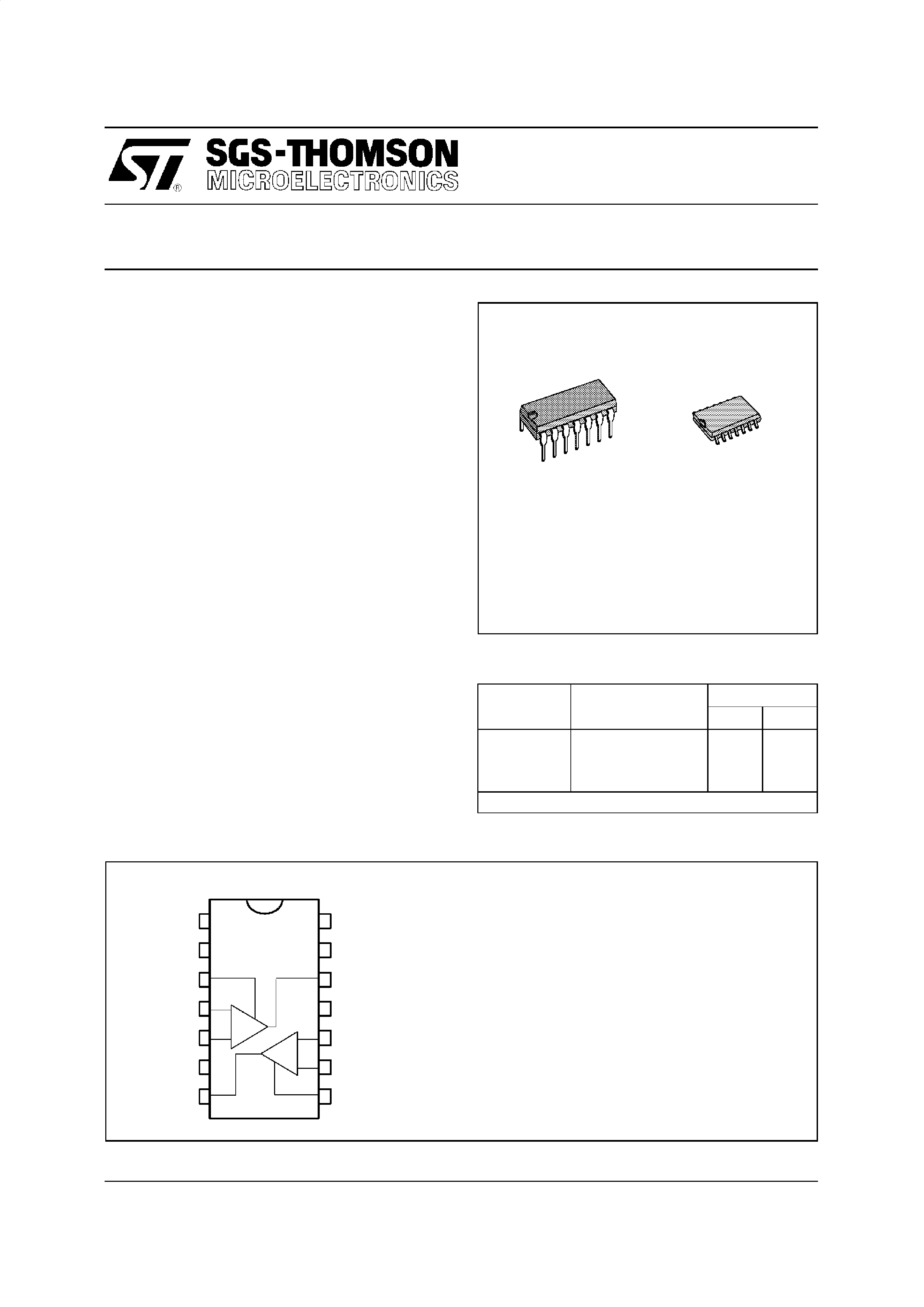
N
DIP14
(Plastic Package)
D
SO14
(Plastic Micropackage)
HIGH SPEED DUAL COMPARATORS
LM119 - LM219
LM319
April 1995
1
2
3
4
8
5
6
7
9
10
11
12
13
14
-
+
-
+
1 - N.C.
2 - N.C.
3 - Ground 1
4 - Non-inverting input 1
5 - Inverting input 1
6- VCC
-
7 - Output 2
PIN CONNECTIONS (top view)
1/9
ABSOLUTE MAXIMUM RATINGS
Symbol
Parameter
LM119
LM219
LM319
Unit
VO -VCC
-
Output to Negative Supply Voltage
36
36
36
V
VCC
-
Negative Supply Voltage
25
25
25
V
VCC
+
Positive Supply Voltage
18
18
18
V
Vid
Differential Input Voltage
±5
±5
±5V
Vi
Input Voltage (note 1)
±15
±15
±15
V
Ptot
Power Dissipation
500
500
500
mW
Toper
Operating Free-air Temperature Range
55 to +125
40 to +105
0 to +70
oC
Tstg
Storage Temperature Range
65 to +150
65 to +150
65 to +150
oC
119-02.TBL
R7
3.5k
R2
R3
R6
R1
Q4
Q3
Q8
4k
4k
3k
3k
Q9
V
CC
V
CC
GND
To other half
Output
Q7
Q6
C1
18
µF
R10
470k
R11
R5
R4
Q2
3k
3k
13k
13k
R12
R8
2k
Q6
Q1
Q22
R9
18k
Q15
Q13
Q10
R15
300
R13
Q14
Q12
Q11
Q16
R16
600
R14
2k
R19
250
R18
1.8k
600
R20
3.6k
R22
60
R23
4k
Q21
Q20
R25
600
R24
250
Q19
Q18
R21
900
Q17
R17
3
Inverting
Input
Non-inverting
Input
119-03.EPS
SCHEMATIC DIAGRAM
LM119 - LM219 - LM319
2/9
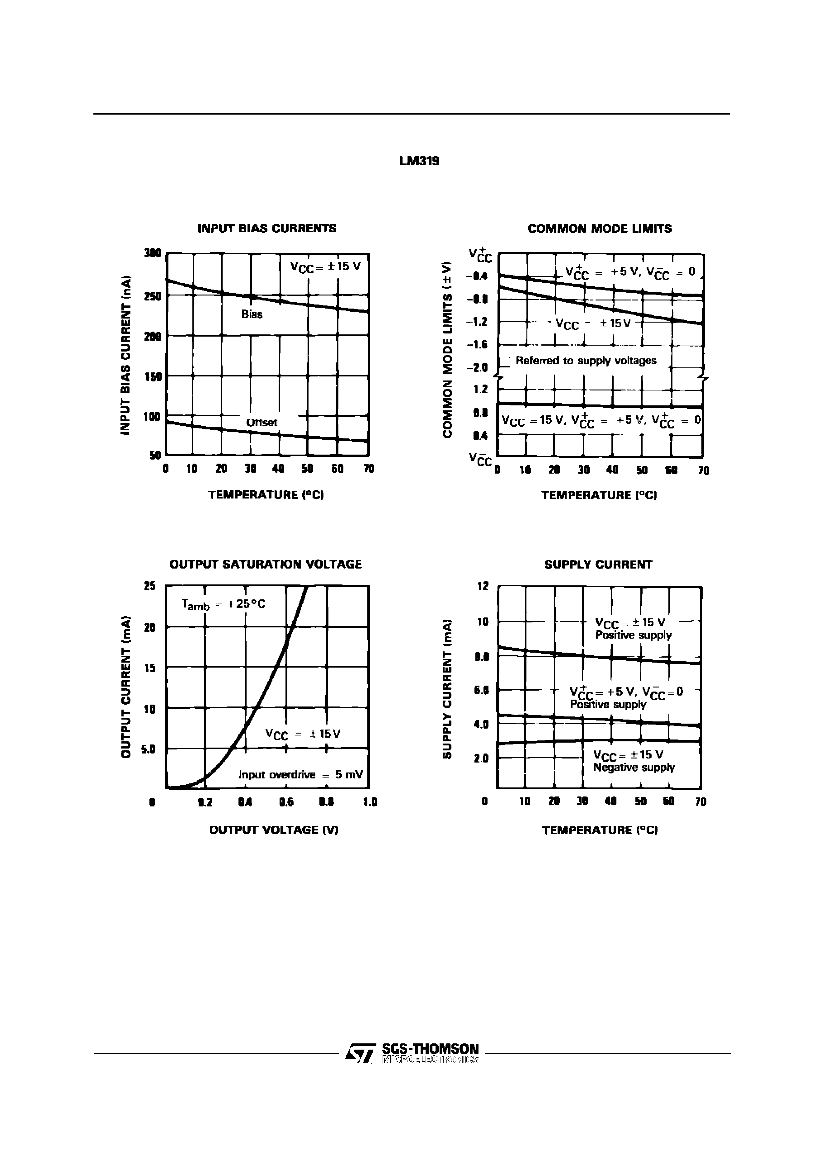
ELECTRICAL CHARACTERISTICS
VCC =
±15V, Tamb =25oC(unless otherwise specified)
Symbol
Parameter
LM119 - LM219
LM319
Unit
Min.
Typ. Max. Min.
Typ. Max.
Vio
Input Offset Voltage (RS
5k) (note 2)
Tamb = +25
oC
Tmin.
Tamb Tmax.
0.7
4
7
28
10
mV
Iio
Input Offset Current (note 2)
Tamb = +25
oC
Tmin.
Tamb Tmax.
30
75
100
80
200
300
nA
Iib
Input Bias Current (note 2)
Tamb = +25
oC
Tmin.
Tamb Tmax.
150
500
1000
250
1000
1200
nA
Avd
Large Signal Voltage Gain
10
40
8
40
V/mV
ICC
+
Positive Supply Current
VCC =
±15V
VCC
+ = +5V, VCC =0V
8
4.3
11.5
8
4.3
12.5
mA
ICC
Negative Supply Current
3
4.5
3
5
mA
Vicm
Input Common Mode Voltage Range
VCC =
±15V
VCC
+ = +5V, V
CC
=0V
±12
1
±13
3
±12
1
±13
3
V
Vid
Differential Input Voltage
±5
±5V
VOL
Low Level Output Voltage
Tamb = +25
oC, IO = 25mA
Vi
5mV
Vi
10mV
Tmin.
Tamb Tmax.
VCC
+ +4.5V, VCC= 0V, IO(sink) < 3.2mA
Vi
6mV
Vi
10mV
0.75
0.23
1.5
0.4
0.75
0.3
1.5
0.4
V
IOH
High Level Output Current (VO = +35V)
Tamb = +25
oCVi 5mV
Vi
10mV
Tmin.
Tamb Tmax.Vi 5mV
0.2
1
2
10
0.2
10
µA
tre
Response Time (note 3)
80
80
ns
119-03.TBL
Notes :
1. F or supply volt ages less than
±15V the absolute maximum input voltage is equal to the supply volt age.
2. T hese specifi cati ons appl y for VCC =
±15V, unless otherwise stated. The offset voltage, offset current and
bi as current specif ic ati ons apply for any supply volt age from a si ngle +5V supply up t o
±15V supplies.
T he off set vol tages and offset current gi ven are the maximum val ues required to drive the output dow n to 1V
or up to +14V wi th a 1mA load current.
T hus, these parameters defi ne an err or band and take in to account the worst case ef fect s of voltage gain
and i nput im pedance.
3. T he response t ime specifi ed i s for a 100mV i nput step w it h 5mV overdr ive.
LM119 - LM219 - LM319
3/9
119-04.EPS
LM119 - LM219 - LM319
4/9
119-05.EPS
LM119 - LM219 - LM319
5/9