AI00761B
16
Q0-Q7
VCC
M27C512
GVPP
VSS
8
A0-A15
E
Figure 1. Logic Diagram
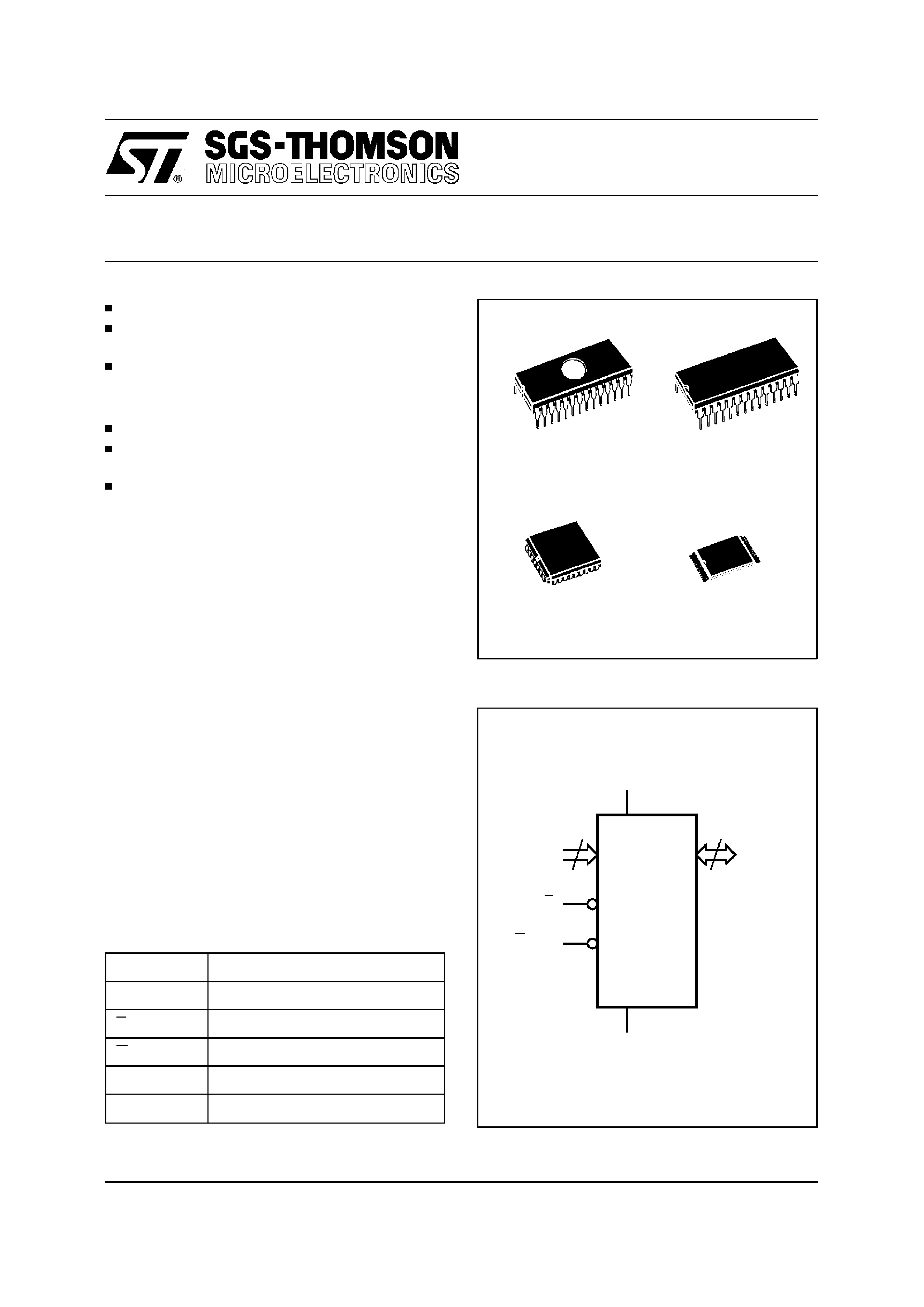
M27C512
512K (64K x 8) UV EPROM and OTP ROM
VERY FAST ACCESS TIME: 60ns
COMPATIBLE with HIGH SPEED
MICROPROCESSORS, ZERO WAIT STATE
LOW POWER "CMOS" CONSUMPTION:
Active Current 30mA
Standby Current 100
µA
PROGRAMMING VOLTAGE: 12.75V
ELECTRONIC SIGNATURE for AUTOMATED
PROGRAMMING
PROGRAMMING TIMES of AROUND 6sec.
(PRESTO IIB ALGORITHM)
DESCRIPTION
The M27C512 is a high speed 524,288 bit UV
erasable and electrically programmable EPROM
ideally suited for applications where fast turn-
around and pattern experimentation are important
requirements. Its is organized as 65,536 by 8 bits.
The 28 pin Window Ceramic Frit-Seal Dual-in-Line
package has transparent lid which allows the user
to expose the chip to ultraviolet light to erase the
bit pattern. Anew pattern can then be written to the
device by following the programming procedure.
For applications where the content is programmed
only one time and erasure is not required, the
M27C512 is offered in Plastic Dual-in-Line, Plastic
Thin Small Outline and Plastic Leaded Chip Carrier
packages.
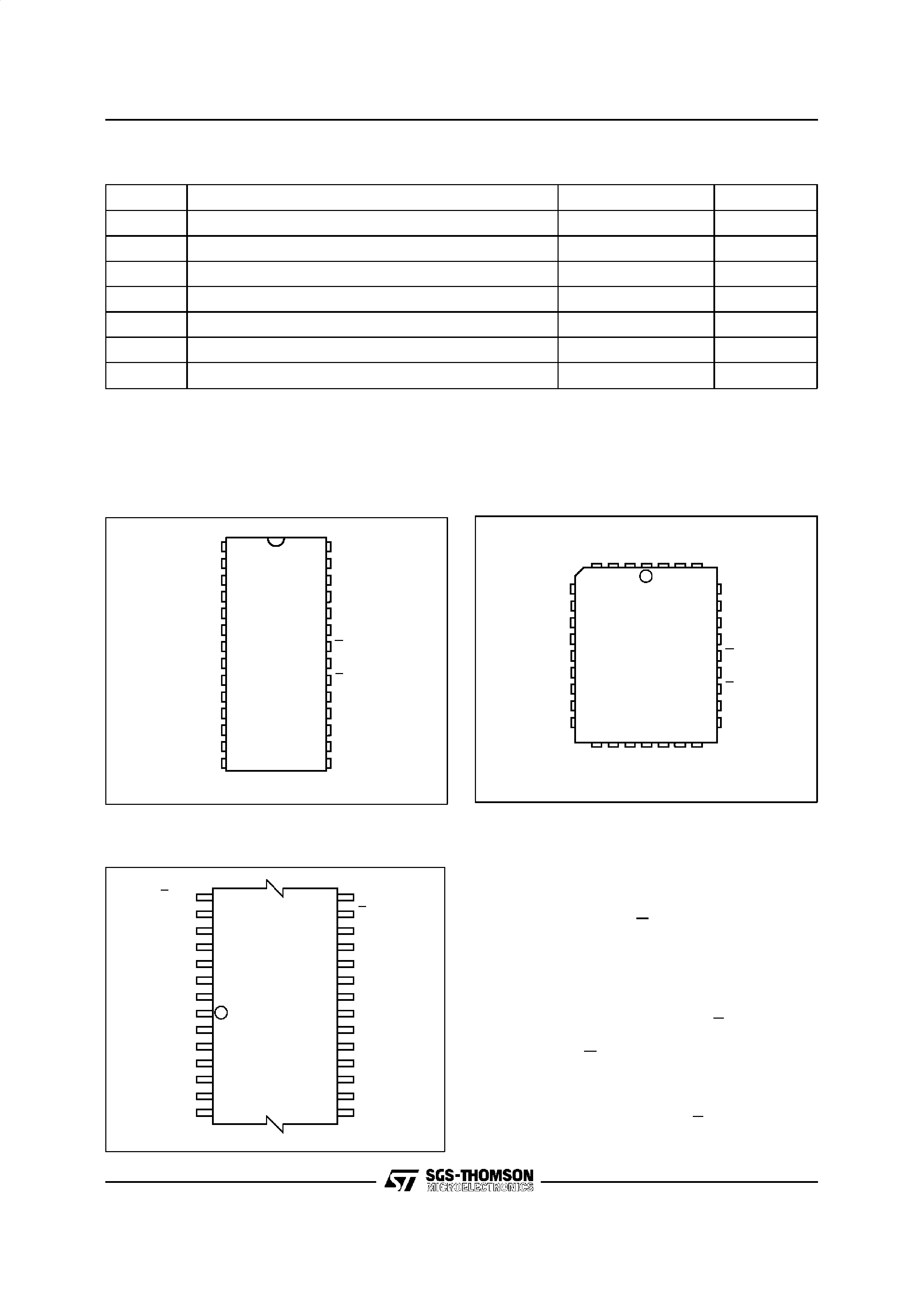
A0 - A15
Address Inputs
Q0 - Q7
Data Outputs
E
Chip Enable
GVPP
Output Enable / Program Supply
VCC
Supply Voltage
VSS
Ground
Table 1. Signal Names
TSOP28 (N)
8 x 13.4mm
PLCC32 (C)
28
1
PDIP28 (B)
1
28
FDIP28W (F)
March 1995
1/14
DEVICE OPERATION
The modes of operationsof the M27C512 are listed
in the Operating Modes table. A single 5V power
supply is required in the read mode. All inputs are
TTL levels except for GVPP and 12V on A9 for
Electronic Signature.
Read Mode
The M27C512 has two control functions, both of
which must be logically active in order to obtain
data at the outputs. Chip Enable (E) is the power
control and should be used for device selection.
Output Enable (G) is the output control and should
be used to gate data to the output pins, inde-
pendent of device selection. Assuming that the
addresses are stable, the address access time
(tAVQV) is equal to the delay from E to output (tELQV).
A1
A0
Q0
A7
A4
A3
A2
A6
A5
A13
A10
A8
A9
Q7
A14
A11
GVPP
E
Q5
Q1
Q2
Q3
VSS
Q4
Q6
A12
A15
VCC
AI00762
M27C512
8
1
2
3
4
5
6
7
9
10
11
12
13
14
16
15
28
27
26
25
24
23
22
21
20
19
18
17
Figure 2A. DIP Pin Connections
Warning: NC = Not Connected, DU = Don't Use
AI00763
A13
A8
A10
Q4
17
A0
NC
Q0
Q1
Q2
DU
Q3
A6
A3
A2
A1
A5
A4
9
A14
A9
1
A15
A11
Q6
A7
Q7
32
DU
V
CC
M27C512
A12
NC
Q5
GVPP
E
25
V
SS
Figure 2B. LCC Pin Connections
A1
A0
Q0
A5
A2
A4
A3
A9
A11
Q7
A8
GVPP
E
Q5
Q1
Q2
Q3
Q4
Q6
A13
A14
A12
A6
A15
VCC
A7
AI00764B
M27C512
28
1
22
78
14
15
21
VSS
A10
Figure 2C. TSOP Pin Connections
Symbol
Parameter
Value
Unit
TA
Ambient Operating Temperature
40 to 125
°C
TBIAS
Temperature Under Bias
50 to 125
°C
TSTG
Storage Temperature
65 to 150
°C
VIO (2)
Input or Output Voltages (except A9)
2 to 7
V
VCC
Supply Voltage
2 to 7
V
VA9
(2)
A9 Voltage
2 to 13.5
V
VPP
Program Supply Voltage
2 to 14
V
Notes: 1. Except for the rating "Operating Temperature Range", stresses above those listed in the Table "Absolute Maximum Ratings"
may cause permanent damage to the device. These are stress ratings only and operation of the device at these or any other
conditions above those indicated in the Operating sections of this specification is not implied. Exposure to Absolute Maximum
Rating conditions for extended periods may affect device reliability. Refer also to the SGS-THOMSON SURE Program and other
relevant quality documents.
2. Minimum DC voltage on Input or Output is 0.5V with possible undershoot to 2.0V for a period less than 20ns. Maximum DC
voltage on Output is VCC +0.5V with possible overshoot to VCC +2V for a period less than 20ns.
Table 2. Absolute Maximum Ratings (1)
2/14
M27C512
Data is available at the output after a delay of tGLQV
from the falling edge of G, assuming that E has
been low and the addresses have been stable for
at least tAVQV-tGLQV.
Standby Mode
The M27C512 has a standby mode which reduces
the active current from 30mA to 100
µAThe
M27C512 is placed in the standby mode by apply-
ing a CMOS high signal to the E input. When in the
standby mode, the outputs are in a high impedance
state, independent of the GVPP input.
Two Line Output Control
Because EPROMs are usually used in larger mem-
ory arrays, the product features a 2 line control
function which accommodates the use of multiple
memory connection. The two line control function
allows:
a. the lowest possible memory power dissipation,
b. complete assurance that output bus contention
will not occur.
For the most efficient use of these two control lines,
E should be decoded and used as the primary
device selecting function, while G should be made
a common connection to all devices in the array
and connected to the READ line from the system
control bus. This ensures that all deselected mem-
ory devices are in their low power standby mode
and that the output pins are only active when data
is required from a particular memory device.
System Considerations
The power switching characteristics of Advanced
CMOS EPROMs require careful decoupling of the
devices. The supply current, ICC, has three seg-
ments that are of interest to the system designer:
the standby current level, the active current level,
and transient current peaks that are produced by
the falling and rising edges of E. The magnitude of
the transient current peaks is dependent on the
capacitive and inductive loading of the device at the
output. The associated transient voltage peaks
can be suppressed by complying with the two line
output control and by properly selected decoupling
capacitors. It is recommended that a 0.1
µF ce-
ramic capacitor be used on every device between
VCC and VSS. This should be a high frequency
capacitor of low inherent inductance and should be
placed as close to the device as possible. In addi-
tion, a 4.7
µF bulk electrolytic capacitor should be
used between VCC and VSS for every eight devices.
The bulk capacitor should be located near the
power supplyconnection point.The purpose of the
bulk capacitor is to overcome the voltage drop
caused by the inductive effects of PCB traces.
Programming
When delivered (and after each erasure for UV
EPROM), all bits of the M27C512 are in the '1'
state. Data is introduced by selectively program-
ming '0' into the desired bit locations. Although only
'0' will be programmed, both '1' and '0' can be
present in the data word. The only way to change
a '0' to a '1' is by die exposure to ultraviolet light
(UV EPROM). The M27C512 is in the program-
ming mode when VPP input is at 12.75V and E is at
Mode
E
GVPP
A9
Q0 - Q7
Read
VIL
VIL
X
Data Out
Output Disable
VIL
VIH
X
Hi-Z
Program
VIL Pulse
VPP
X
Data In
Program Inhibit
VIH
VPP
X
Hi-Z
Standby
VIH
X
X
Hi-Z
Electronic Signature
VIL
VIL
VID
Codes
Note:X = VIH or VIL,VID = 12V
± 0.5V
Table 3. Operating Modes
Identifier
A0
Q7
Q6
Q5
Q4
Q3
Q2
Q1
Q0
Hex Data
Manufacturer's Code
VIL
0
010
0
000
20h
Device Code
VIH
0
011
1
101
3Dh
Table 4. Electronic Signature
DEVICE OPERATION (cont'd)
3/14
M27C512
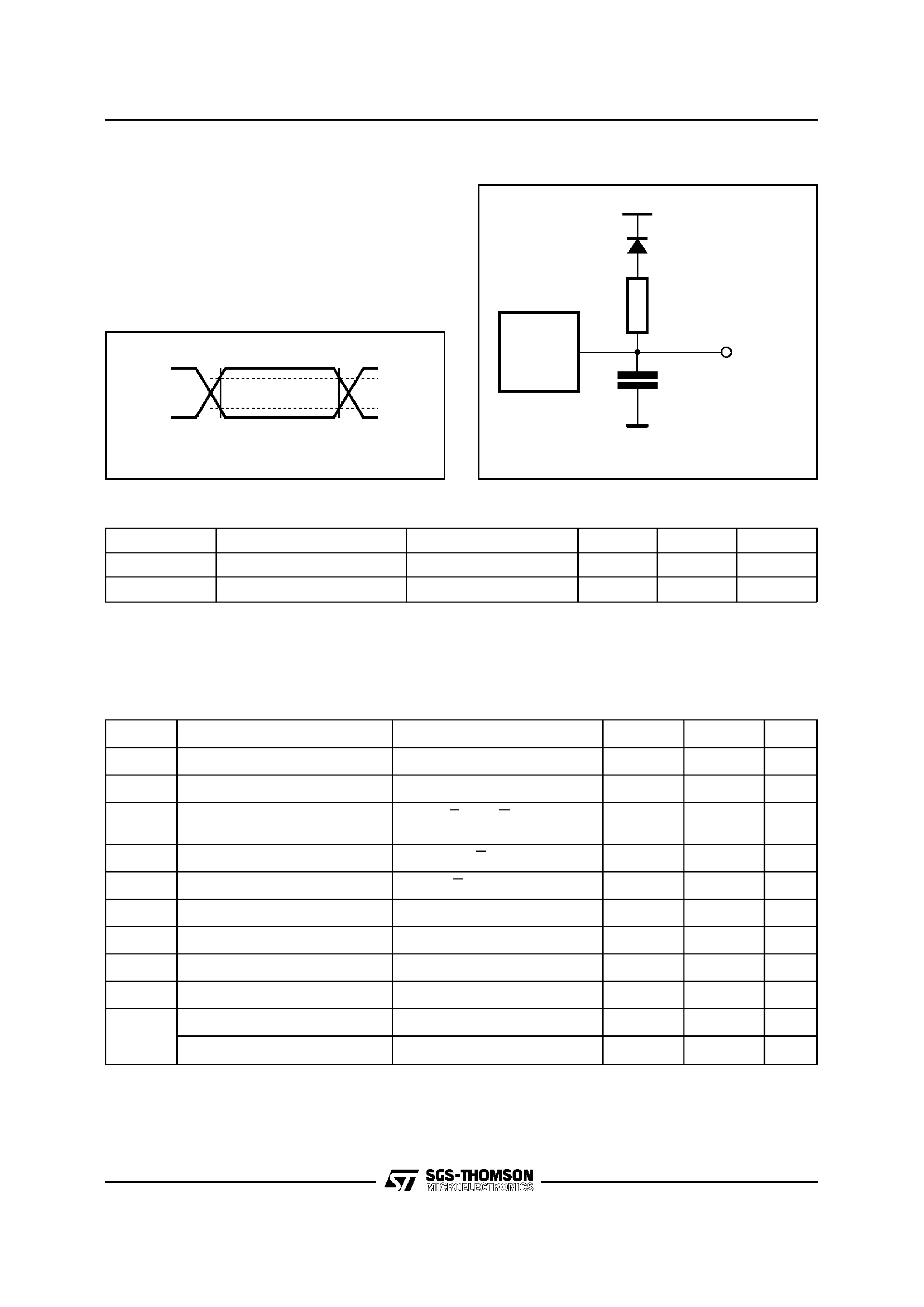
AI00826
2.4V
0.4V
2.0V
0.8V
Figure 3. AC Testing Input Output Waveforms
Input Rise and Fall Times
20ns
Input Pulse Voltages
0.4V to 2.4V
Input and Output Timing Ref. Voltages
0.8V to 2.0V
AC MEASUREMENT CONDITIONS
AI00828
1.3V
OUT
CL = 100pF
CL includes JIG capacitance
3.3k
1N914
DEVICE
UNDER
TEST
Figure 4. AC Testing Load Circuit
Note that Output Hi-Z is defined as the point where data
is no longer driven.
Symbol
Parameter
Test Condition
Min
Max
Unit
CIN
Input Capacitance
VIN =0V
6
pF
COUT
Output Capacitance
VOUT =0V
12
pF
Note. 1. Sampled only, not 100% tested.
Table 5. Capacitance (1) (TA =25
°C, f = 1 MHz )
Symbol
Parameter
Test Condition
Min
Max
Unit
ILI
Input Leakage Current
0V
VIN VCC
±10
µA
ILO
Output Leakage Current
0V
VOUT VCC
±10
µA
ICC
Supply Current
E= VIL,G = VIL,
IOUT = 0mA, f = 5MHz
30
mA
ICC1
Supply Current (Standby) TTL
E = VIH
1mA
ICC2
Supply Current (Standby) CMOS
E > VCC 0.2V
100
µA
IPP
Program Current
VPP =VCC
10
µA
VIL
Input Low Voltage
0.3
0.8
V
VIH
(2)
Input High Voltage
2
VCC +1
V
VOL
Output Low Voltage
IOL = 2.1mA
0.4
V
VOH
Output High Voltage TTL
IOH = 1mA
3.6
V
Output High Voltage CMOS
IOH = 100
µAVCC 0.7V
V
Notes: 1. VCC must be applied simultaneously with or before VPP and removed simultaneously or after VPP.
2. Maximum DC voltage on Output is VCC +0.5V.
Table 6. Read Mode DC Characteristics (1)
(TA = 0 to 70
°C, 40 to 85 °C or 40 to 125 °C; VCC =5V ± 5% or 5V ± 10%; VPP =VCC)
4/14
M27C512
Symbol
Alt
Parameter
Test Condition
M27C512
Unit
-60
-70
-80
-90
Min
Max
Min
Max
Min
Max
Min
Max
tAVQV
tACC
Address Valid to
Output Valid
E= VIL,G = VIL
60
70
80
90
ns
tELQV
tCE
Chip Enable Low to
Output Valid
G= VIL
60
70
80
90
ns
tGLQV
tOE
Output Enable Low to
Output Valid
E= VIL
30
35
40
40
ns
tEHQZ
(2)
tDF
Chip Enable High to
Output Hi-Z
G= VIL
0
25
0
30
0
30
0
30
ns
tGHQZ
(2)
tDF
Output Enable High to
Output Hi-Z
E= VIL
0
25
0
30
0
30
0
30
ns
tAXQX
tOH
Address Transition to
Output Transition
E= VIL,G = VIL
0
000
ns
Table 7A. Read Mode AC Characteristics (1)
(TA = 0 to 70
°C, 40 to 85 °C or 40 to 125 °C; VCC =5V ± 5% or 5V ± 10%; VPP =VCC)
Symbol
Alt
Parameter
Test Condition
M27C512
Unit
-10
-12
-15/-20/-25
Min
Max
Min
Max
Min
Max
tAVQV
tACC
Address Valid to Output Valid
E = VIL,G = VIL
100
120
150
ns
tELQV
tCE
Chip Enable Low to Output Valid
G = VIL
100
120
150
ns
tGLQV
tOE
Output Enable Low to Output Valid
E = VIL
40
50
60
ns
tEHQZ
(2)
tDF
Chip Enable High to Output Hi-Z
G = VIL
0
30
0
40
0
50
ns
tGHQZ
(2)
tDF
Output Enable High to Output Hi-Z
E = VIL
0
30
0
40
0
50
ns
tAXQX
tOH
Address Transition to
Output Transition
E=VIL,G = VIL
000
ns
Notes. 1. VCC must be applied simultaneously with or before VPP and removed simultaneously or after VPP.
2. Sampled only, not 100% tested.
Table 7B. Read Mode AC Characteristics (1)
(TA = 0 to 70
°C, 40 to 85 °C or 40 to 125 °C; VCC =5V ± 5% or 5V ± 10%; VPP =VCC)
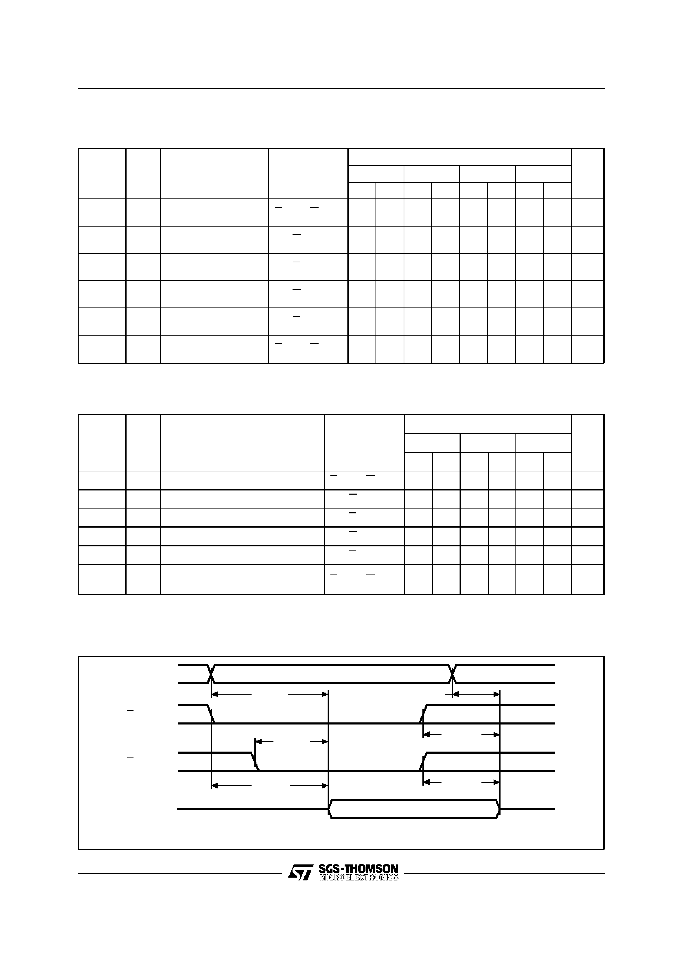
AI00735
tAXQX
tEHQZ
DATA OUT
A0-A15
E
G
Q0-Q7
tAVQV
tGHQZ
tGLQV
tELQV
VALID
Hi-Z
Figure 5. Read Mode AC Waveforms
5/14
M27C512