AI00767B
15
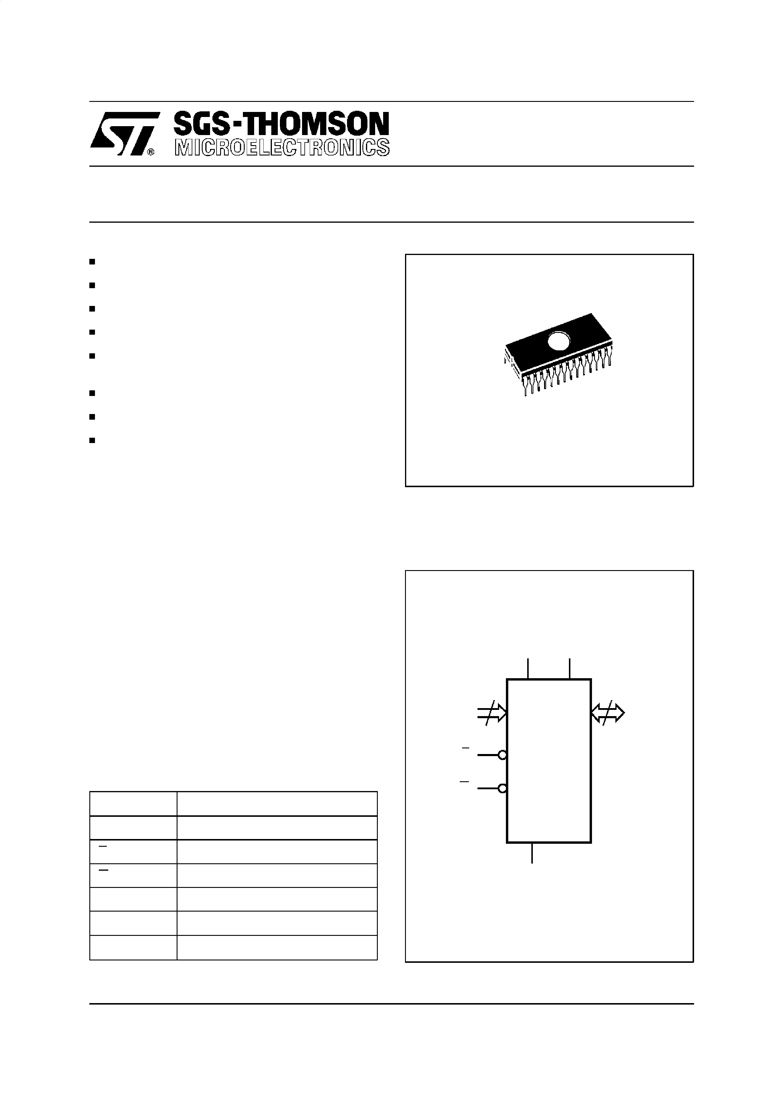
A0-A14
Q0-Q7
VPP
VCC
M27256
G
E
VSS
8
Figure 1. Logic Diagram
M27256
NMOS 256K (32K x 8) UV EPROM
FAST ACCESS TIME: 170ns
EXTENDED TEMPERATURE RANGE
SINGLE 5V SUPPLY VOLTAGE
LOW STANDBY CURRENT: 40mA max
TTL COMPATIBLE DURING READ and
PROGRAM
FAST PROGRAMMING ALGORITHM
ELECTRONIC SIGNATURE
PROGRAMMING VOLTAGE: 12V
DESCRIPTION
The M27256 is a 262,144 bit UV erasable and
electrically programmable memory EPROM. It is
organized as 32.768 words by 8 bits.
The M27256 is housed in a 28 pin Window Ceramic
Frit-Seal Dual-in-Line package. The transparent lid
allows the user to expose the chip to ultraviolet light
to erase the bit pattern. A new pattern can then be
written to the device by following the programming
procedure.
A0 - A14
Address Inputs
Q0 - Q7
Data Outputs
E
Chip Enable
G
Output Enable
VPP
Program Supply
VCC
Supply Voltage
VSS
Ground
Table 1. Signal Names
1
28
FDIP28W (F)
March 1995
1/10
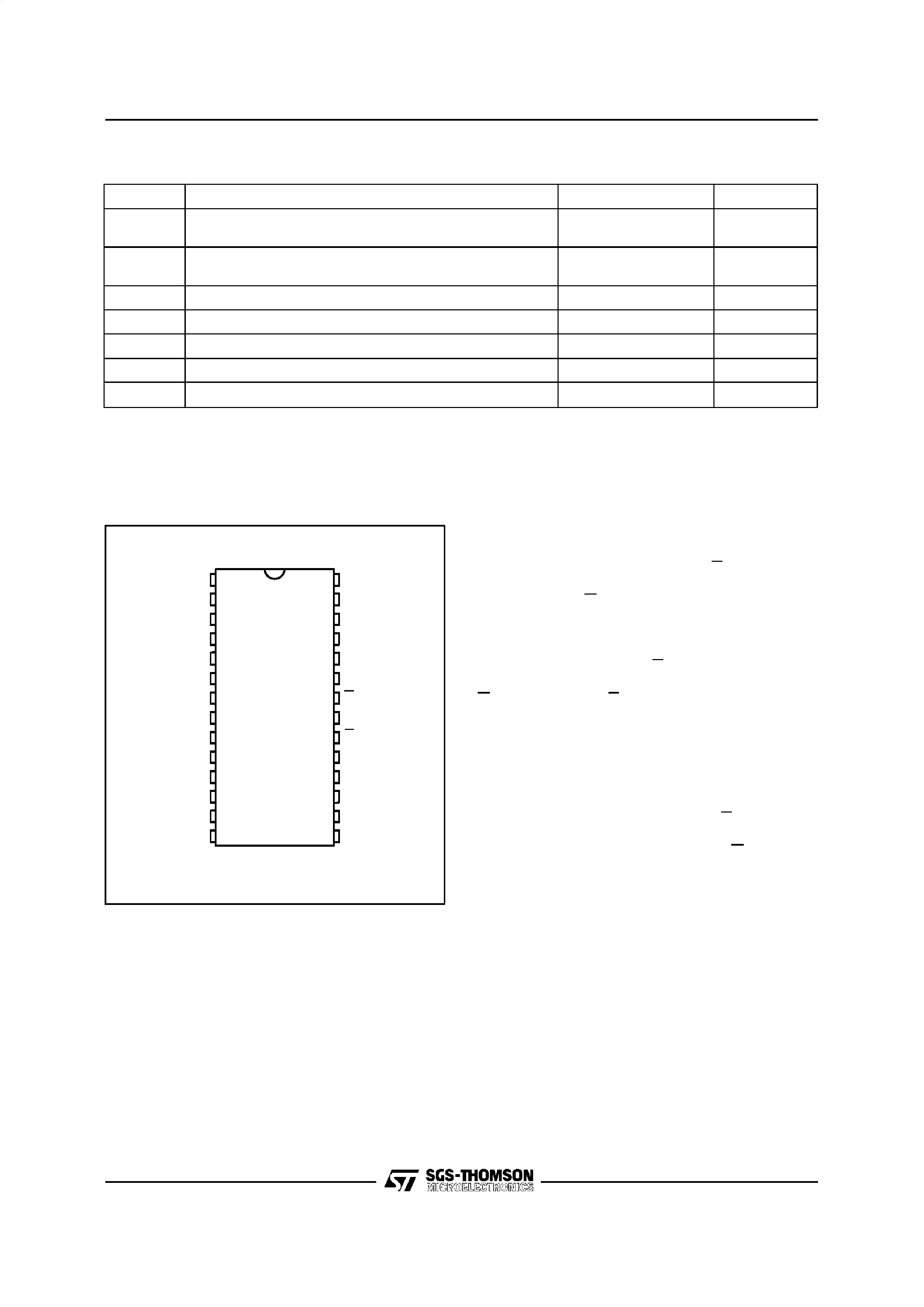
A1
A0
Q0
A7
A4
A3
A2
A6
A5
A13
A10
A8
A9
Q7
A14
A11
G
E
Q5
Q1
Q2
Q3
VSS
Q4
Q6
A12
VPP
VCC
AI00768
M27256
8
1
2
3
4
5
6
7
9
10
11
12
13
14
16
15
28
27
26
25
24
23
22
21
20
19
18
17
Figure 2. DIP Pin Connections
Symbol
Parameter
Value
Unit
TA
Ambient Operating Temperature
grade 1
grade 6
0to 70
40 to 85
°C
TBIAS
Temperature Under Bias
grade 1
grade 6
10 to 80
50 to 95
°C
TSTG
Storage Temperature
65 to 125
°C
VIO
Input or Output Voltages
0.6 to 6.25
V
VCC
Supply Voltage
0.6 to 6.25
V
VA9
VA9 Voltage
0.6 to 13.5
V
VPP
Program Supply
0.6 to 14
V
Note: Except for the rating "Operating Temperature Range", stresses above those listed in the Table "Absolute Maximum Ratings" may cause
permanent damage to the device. These are stress ratings only and operation of the device at these or any other conditions above those
indicated in the Operating sections of this specification is not implied. Exposure to Absolute Maximum Rating conditions for extended periods
may affect device reliability. Refer also to the SGS-THOMSON SURE Program and other relevant quality documents.
Table 2. Absolute Maximum Ratings
DEVICE OPERATION
The eight modes of operations of the M27256 are
listed in the Operating Modes Table. A single 5V
power supply is required in the read mode. All
inputs are TTL levels except for VPP and 12V on A9
for Electronic Signature.
Read Mode
The M27256 has two control functions, both of
which must be logically satisfied in order to obtain
data at the outputs. Chip Enable (E) is the power
control and should be used for device selection.
Output Enable (G) is the output control and should
be used to gate data to the output pins, inde-
pendent of device selection. Assuming that the
addresses are stable, address access time (tAVQV)
is equal to the delay from E to output (tELQV). Data
is available at the outputs after the falling edge of
G, assuming that E has been low and the ad-
dresses have been stable for at least tAVQV-tGLQV.
Standby Mode
The M27256 has a standby mode which reduces
the maximum active power current from 100mA to
40mA. The M27256 is placed in the standby mode
by applying a TTL high signal to the E input. When
in the standby mode, the outputs are in a high
impedance state, independent of the G input.
Two Line Output Control
Because EPROMs are usually used in larger mem-
ory arrays, this product features a 2 line control
function which accommodates the use of multiple
memory connection. The two line control function
allows:
a. the lowest possible memory power dissipation,
b. complete assurance that output bus contention
will not occur.
2/10
M27256
For the most efficient use of these two control lines,
E should be decoded and used as the primary
device selecting function, while G should be made
a common connection to all devices in the array
and connected to the READ line from the system
control bus.
This ensures that all deselected memory devices
are in their low power standby mode and that the
output pins are only active when data is required
from a particular memory device.
System Considerations
The power switching characteristics of fast
EPROMs require careful decouplingof the devices.
The supply current, ICC, has three segments that
are of interest to the system designer : the standby
current level, the active current level, and transient
current peaks that are produced by the falling and
rising edges of E. The magnitude of the transient
current peaks is dependent on the capacitive and
inductive loading of the device at the output. The
associated transient voltage peaks can be sup-
pressed by complying with the two line output
control and by properly selected decoupling ca-
pacitors. It is recommended that a 1
µF ceramic
capacitor be used on every device between VCC
and VSS. This should be a high frequency capacitor
of low inherent inductance and should be placed
as close to the device as possible. In addition, a
4.7
µF bulk electrolytic capacitors should be used
between VCC and VSS for every eight devices. The
bulk capacitor should be located near the power
supply connection point. The purpose of the bulk
capacitor is to overcome the voltage drop caused
by the inductive effects of PCB traces.
Programmain
When delivered, (and after each erasure for UV
EPROM), all bits of the M27256 are in the "1" state.
Data is introduced by selectively programming "0s"
into the desired bit locations. Although only "0s" will
be programmed, both "1s" and "0s" can be present
in the data word. The only way to change a "0" to
a "1" is by ultraviolet light erasure. The M27256 is
in the programming mode when VPP input is at
12.5V and E is at TTL low. The data to be pro-
grammed is applied 8 bits in parallel to the data
output pins. The levels required for the address and
data inputs are TTL.
Fast Programming Algorithm
Fast Programming Algorithm rapidly programs
M27256 EPROMs using an efficient and reliable
method suited to the production programming en-
vironment. Programming reliability is also ensured
as the incremental program margin of each byte is
continually monitored to determine when it has
been successfully programmed. A flowchart of the
M27256 Fast Programming Algorithm is shown on
the Flowchart. The Fast Programming Algorithm
utilizes two different pulse types : initial and over-
program. The duration of the initial E pulse(s) is
1ms, which will then be followed by a longer over-
program pulse of length 3ms by n (n is equal to the
number of the initial one millisecond pulses applied
Mode
E
G
A9
VPP
Q0 - Q7
Read
VIL
VIL
XVCC
Data Out
Output Disable
VIL
VIH
XVCC
Hi-Z
Program
VIL Pulse
VIH
XVPP
Data In
Verify
VIH
VIL
XVPP
Data Out
Optional Verify
VIL
VIL
XVPP
Data Out
Program Inhibit
VIH
VIH
XVPP
Hi-Z
Standby
VIH
XX
VCC
Hi-Z
Electronic Signature
VIL
VIL
VID
VCC
Codes
Note: X= VIH or VIL,VID = 12V
± 0.5%.
Table 3. Operating Modes
Identifier
A0
Q7
Q6
Q5
Q4
Q3
Q2
Q1
Q0
Hex Data
Manufacturer's Code
VIL
00100
000
20h
Device Code
VIH
00000
100
04h
Table 4. Electronic Signature
DEVICE OPERATION (cont'd)
3/10
M27256
AI00827
2.4V
0.45V
2.0V
0.8V
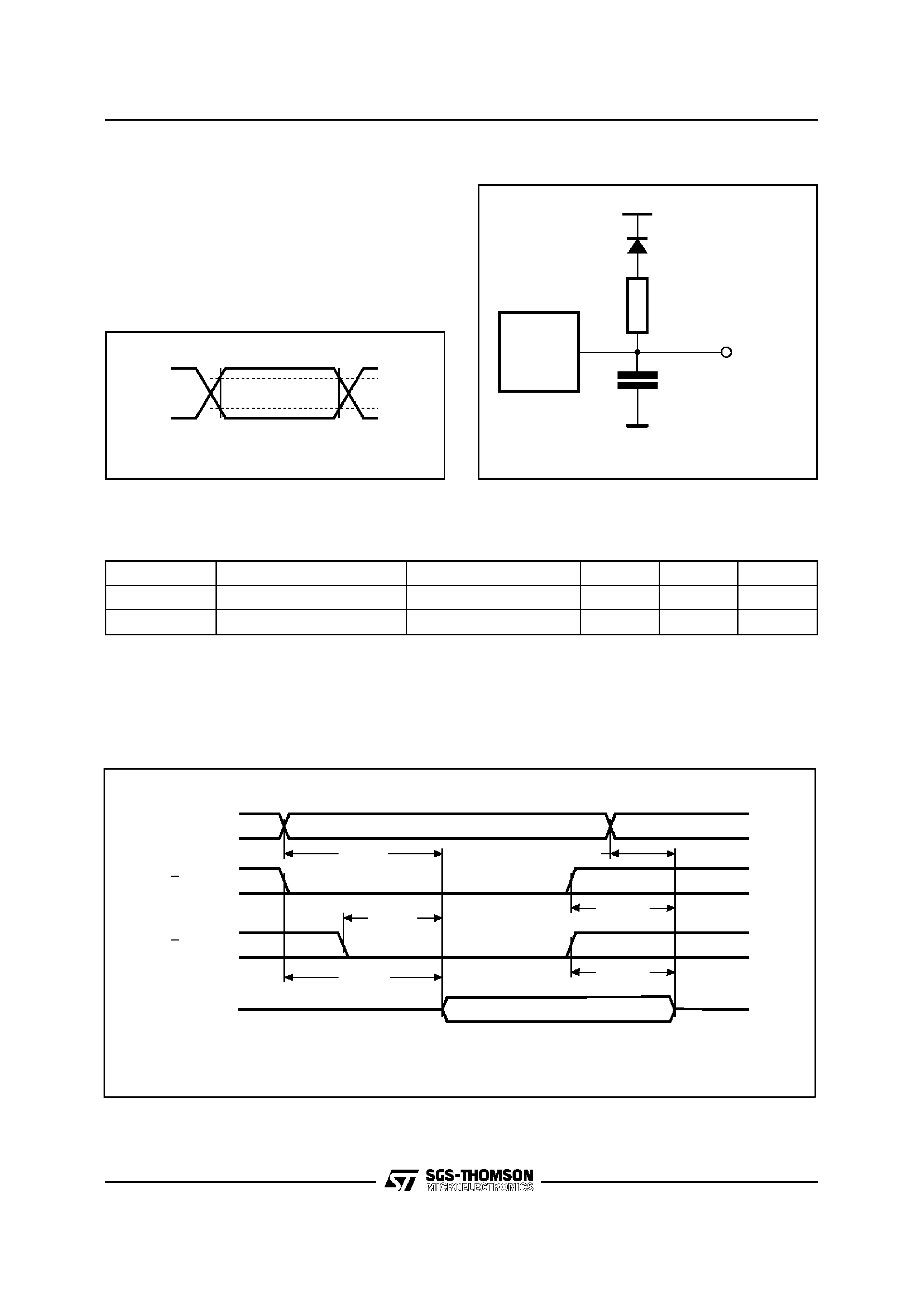
Figure 3. AC Testing Input Output Waveforms
Input Rise and Fall Times
20ns
Input Pulse Voltages
0.45V to 2.4V
Input and Output Timing Ref. Voltages
0.8V to 2.0V
AC MEASUREMENT CONDITIONS
AI00828
1.3V
OUT
CL = 100pF
CL includes JIG capacitance
3.3k
1N914
DEVICE
UNDER
TEST
Figure 4. AC Testing Load Circuit
Note that Output Hi-Z is defined as the point where data
is no longer driven.
Symbol
Parameter
Test Condition
Min
Max
Unit
CIN
Input Capacitance
VIN =0V
6
pF
COUT
Output Capacitance
VOUT =0V
12
pF
Note: 1. Sampled only, not 100% tested.
Table 5. Capacitance (1) (TA =25
°C, f = 1 MHz )
AI00758
tAXQX
tEHQZ
DATA OUT
A0-A14
E
G
Q0-Q7
tAVQV
tGHQZ
tGLQV
tELQV
VALID
Hi-Z
Figure 5. Read Mode AC Waveforms
4/10
M27256
Symbol
Alt
Parameter
Test
Condition
M27256
Unit
-1
-2, -20
blank, -25
Min
Max
Min
Max
Min
Max
tAVQV
tACC
Address Valid to
Output Valid
E= VIL,
G= VIL
170
200
250
ns
tELQV
tCE
Chip Enable Low
to Output Valid
G= VIL
170
200
250
ns
tGLQV
tOE
Output Enable
Low to Output Valid
E=VIL
70
75
100
ns
tEHQZ
(2)
tDF
Chip Enable High
to Output Hi-Z
G= VIL
035
0
55
060
ns
tGHQZ
(2)
tDF
Output Enable
High to Output Hi-Z
E=VIL
035
0
55
060
ns
tAXQX
tOH
Address Transition
to Output Transition
E= VIL,
G= VIL
000
ns
Table 7A. Read Mode AC Characteristics (1)
(TA = 0 to 70
°C or 40 to 85 °C; VCC =5V ± 5% or 5V ± 10%; VPP =VCC)
Symbol
Parameter
Test Condition
Min
Max
Unit
ILI
Input Leakage Current
0
VIN VCC
±10
µA
ILO
Output Leakage Current
VOUT =VCC
±10
µA
ICC
Supply Current
E = VIL,G = VIL
100
mA
ICC1
Supply Current (Standby)
E = VIH
40
mA
IPP
Program Current
VPP =VCC
5mA
VIL
Input Low Voltage
0.1
0.8
V
VIH
Input High Voltage
2
VCC +1
V
VOL
Output Low Voltage
IOL = 2.1mA
0.45
V
VOH
Output High Voltage
IOH = 400
µA
2.4
V
Note: 1. VCC must be applied simultaneously with or before VPP and removed simultaneously or after VPP.
Table 6. Read Mode DC Characteristics
(1)
(TA = 0 to 70
°C or 40 to 85 °C; VCC =5V ± 5% or 5V ± 10%; VPP =VCC)
Symbol
Alt
Parameter
Test
Condition
M27256
Unit
-3
-4
Min
Max
Min
Max
tAVQV
tACC
Address Valid to
Output Valid
E= VIL,
G= VIL
300
450
ns
tELQV
tCE
Chip Enable Low
to Output Valid
G= VIL
300
450
ns
tGLQV
tOE
Output Enable
Low to Output Valid
E= VIL,
120
150
ns
tEHQZ
(2)
tDF
Chip Enable High
to Output Hi-Z
G= VIL
0
105
0
130
ns
tGHQZ
(2)
tDF
Output Enable
High to Output Hi-Z
E=VIL
0
105
0
130
ns
tAXQX
tOH
Address Transition
to Output Transition
E= VIL,
G= VIL
00
ns
Notes: 1. VCC must be applied simultaneously with or before VPP and removed simultaneously or after VPP.
2. Sampled only, not 100% tested.
Table 7B. Read Mode AC Characteristics (1)
(TA = 0 to 70
°C or 40 to 85 °C; VCC =5V ± 5% or 5V ± 10%; VPP =VCC)
5/10
M27256