LOW POWER DUAL VOLTAGE COMPARATORS
.
WIDE SINGLE SUPPLY VOLTAGE RANGE OR
DUAL SUPPLIES +2V TO +36V OR
±1V TO
±18V
.
VERY LOW SUPPLY CURRENT (0.4mA)
INDEPENDENT OF SUPPLY VOLTAGE
(1 mW/comparator at +5V)
.
LOW INPUT BIAS CURRENT : 25nA TYP
.
LOW INPUT OFFSET CURRENT :
±5nA TYP
.
LOW INPUT OFFSET VOLTAGE :
±1mV TYP
.
INPUT COMMON-MODE VOLTAGE RANGE
INCLUDES GROUND
.
LOW OUTPUT SATURATION VOLTAGE :
250mV TYP. (IO = 4mA)
.
DIFFERENTIAL INPUT VOLTAGE RANGE
EQUAL TO THE SUPPLY VOLTAGE
.
TTL, DTL, ECL, MOS, CMOS COMPATIBLE
OUTPUTS
DESCRIPTION
These devices consist of two independent low
power voltage comparators designed specifically to
operate from a single supply over a wide range of
voltages. Operation from split power supplies is also
possible.
These comparators also have a unique characteris-
tic in that the input common-mode voltage range
includes ground even though operated from a single
power supply voltage.
ORDER CODES
Part
Number
Temperature
Range
Package
ND
LM193
55, +125
oC
··
LM293
40, +105
oC
··
LM393
0, +70
oC
··
Example : LM393D
193-01.TBL
1 - Output 1
2 - Inverting input 1
3 - Non-inverting input 1
4- VCC
-
5 - Non-inverting input 2
6 - Inverting input 2
7 - Output 2
8- VCC
+
PIN CONNECTIONS (top views)
1
2
3
45
6
7
8
-
+
-
+
193-01.EPS
DIP8/SO8
LM193 - LM293
LM393
October 1994
N
DIP8
(Plastic Package)
D
SO8
(Plastic Micropackage)
1/9
ABSOLUTE MAXIMUM RATINGS
Symbol
Parameter
LM193
LM293
LM393
Unit
VCC
Supply Voltage
±18 or 36
±18 or 36
±18 or 36
V
Vid
Differential Input Voltage
±36
±36
±36
V
Vi
Input Voltage
0.3 to +36
0.3 to +36
0.3 to +36
V
Output Short-circuit to Ground (note 1)
Infinite
Ptot
Power Dissipation
830
mW
Toper
Operating Free-air TemperatureRange
55 to +125
40 to +105
0 to +70
oC
Tstg
Storage Temperature Range
65 to +150
65 to +150
65 to +150
oC
193-02.TBL
Notes :
1. Short- circui t from the output to VCC
+ can cause excessive heating and eventual destruction. The maximum output
current i s approximately 20mA, independent of the magnitude of VCC
+.
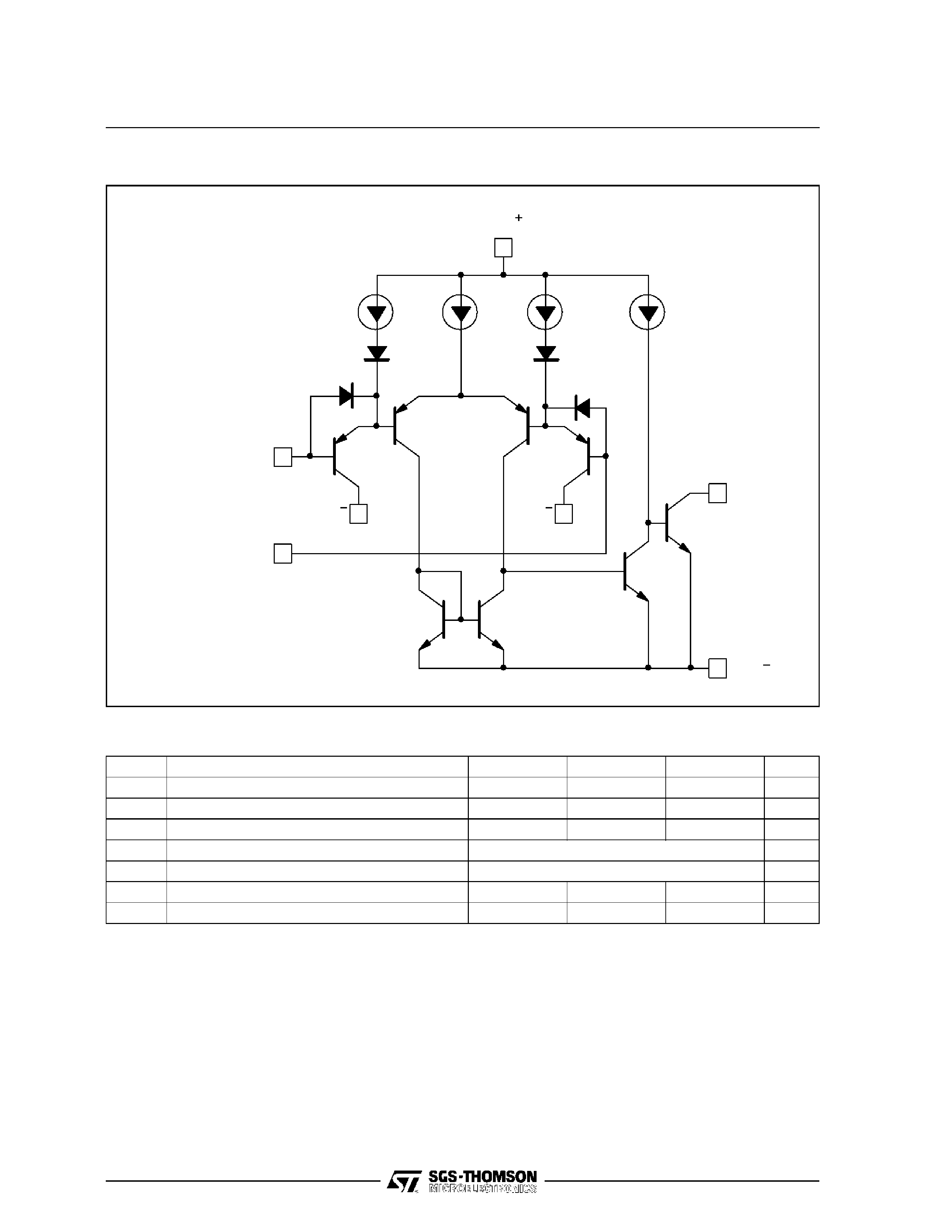
Non-inverting
Input
Inverting
Input
3.5
µA
100
µA
3.5
µA
100
µA
CC
V
CC
V
CC
V
CC
V
O
V
193-02.EPS
SCHEMATIC DIAGRAM (1/2 LM193)
LM193 - LM293 - LM393
2/9
ELECTRICAL CHARACTERISTICS
VCC
+ = +5V, VCC = 0V, Tamb =25oC (unless otherwise specified)
Symbol
Parameter
LM193 - LM293 - LM393
Unit
Min.
Typ.
Max.
Vio
Input Offset Voltage (note 2)
Tamb = +25
oC
Tmin.
Tamb Tmax.
15
9
mV
Iib
Input Bias Current (note 3)
Tamb = +25
oC
Tmin.
Tamb Tmax.
25
250
400
nA
Iio
Input Offset Current
Tamb = +25
oC
Tmin.
Tamb Tmax.
550
150
nA
Avd
Large Signal Voltage Gain
VCC = 15V, RL = 15k
,Vo = 1 to 11V
50
200
V/mV
ICC
Supply Current (all comparators)
VCC = 5V, no load
VCC = 30V, no load
0.4
1
1
2.5
mA
Vicm
Input Common Mode Voltage Range - (note 4)
Tamb = +25
oC
Tmin.
Tamb Tmax.
0
0
VCC
+ -1.5
VCC
+ -2
V
Vid
Differential Input Voltage - (note 6)
VCC
+
V
Isink
Output Sink Current
(Vid = -1V, VO = 1.5V)
6
16
mA
VOL
Low Level Output Voltage
(Vid = -1V, Isink = 4mA)
Tamb =25
oC
Tmin.
Tamb Tmax
250
400
700
mV
IOH
High Level Output Current
(Vid = 1V, VCC =VO = 30V)
Tamb =25
oC
Tmin.
Tamb Tmax
0.1
1
nA
µA
tre
Response Time
(RL = 5.1k
to VCC+) (note 5)
1.3
µs
trel
Large Signal Response Time
(Vi = TTL, Vref = +1.4 V, RL = 5.1k
to VCC+)
300
ns
Notes :
2. At output switch poi nt, VO
1.4V, RS =0 with VCC+ from 5V to 30V and over the full input common-mode range
(0V t o VCC
+ 1.5V).
3. T he directi on of the input curr ent i s out of the IC due to the PNP input stage. T his cur rent is essenti ally constant,
independent of the st ate of the output , so no loading char ge exists on t he reference or input lines.
4. T he input common-mode voltage of either input si gnal vol tage should not be allowed to go negati ve by more t han
0.3V.
T he upper end of the common-mode volt age range is VCC
+ 1.5V, but ei ther or both inputs can go to +30V without
damage.
5. T he response time specifi ed is for a 100mV input step with 5mV overdr ive. For lar ger overdri ve si gnal s 300ns
can be obtai ned.
6. Posi tive excursions of input vol tage may exceed the power supply level . As l ong as the other volt age remai ns
wi thin the common- mode range the comparator will provi de a proper output state. The low input voltage stat e must
not be less t han 0.3V ( or 0. 3V bel ow the negati ve power supply, i f used).
193-03.TBL
LM193 - LM293 - LM393
3/9
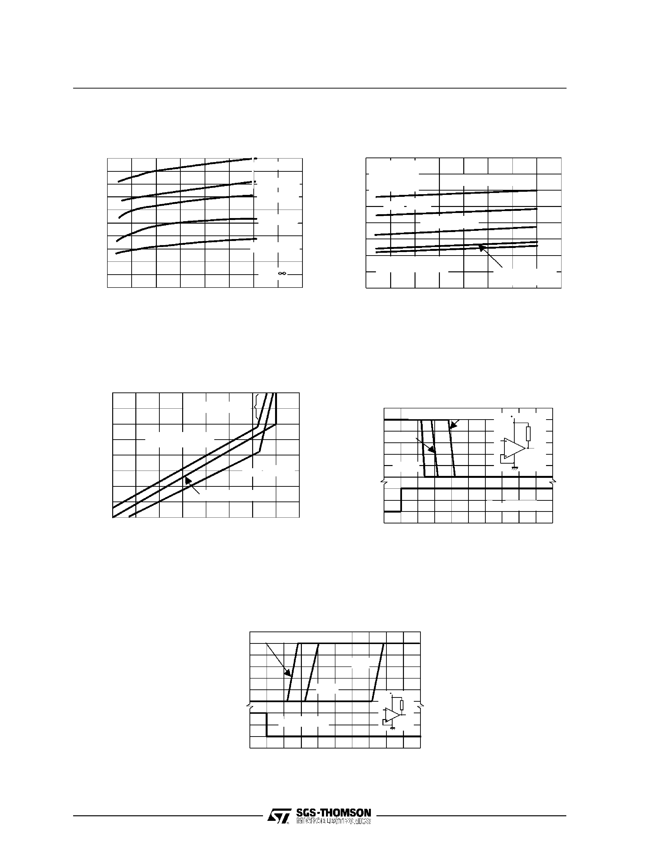
SUPPLY
CURRENT
(mA)
1
0.8
0.6
0.4
0.2
0
10
20
30
40
SUPPLY VOLTAGE (V)
Tamb =+70°C
Tamb = +125
°C
T
= +25
°C
Tamb =0
°C
Tamb =-55
°C
R =
L
193-03.EPS
SUPPLY CURRENT versus
SUPPLY VOLTAGE
INPUT
CURRENT
(nA)
20
10
20
30
40
SUPPLY VOLTAGE (V)
Tamb = +70
°C
Tamb = +125
°C
Tamb = -55
°C
40
60
80
0
Tamb =0
°C
Tamb= +25
°C
V= 0V
i
R= 10
i
9
193-04.EPS
INPUT CURRENT versus
SUPPLY VOLTAGE
Tamb = -55
°C
Tamb = +125
°C
Tamb = +25
°C
Out of saturation
10
1
10
-3
10
-2
10
-1
10
0
SATURATION
VOLTAGE
(V)
10
-2
10
-1
10
0
10
1
10
2
OUTPUT SINK CURRENT (mA)
193-05.EPS
OUTPUT SATURATION VOLTAGE
versus OUTPUT CURRENT
5V
5.1k
e o
e
I
6
5
4
3
2
1
0
0
-50
-100
INPUT
VOLTAGE
(mV)
OUTPUT
VOLTAGE
(V)
0
0.5
1
1.5
2
TIME (
µs)
Input overdrive : 5mV
20mV
100mV
Tamb= +25
°C
193-06.EPS
RESPONSE TIME FOR VARIOUS INPUT
OVERDRIVES - NEGATIVE TRANSITION
5V
5.1 k
eo
e
I
6
5
4
3
2
1
0
100
50
INPUT
VOLTAGE
(mV)
OUTPUT
VOLTAGE
(V)
0
0.5
1
1.5
2
TIME (
µs)
Input overdrive : 100mV
20mV
5mV
Tamb= +25
°C
0
193-07.EPS
RESPONSE TIME FOR VARIOUS INPUT
OVERDRIVES - POSITIVE TRANSITION
LM193 - LM293 - LM393
4/9
V
CC
=5V
15k
V O
+V
(ref)
-V
(ref)
1/2
LM193
193-08.EPS
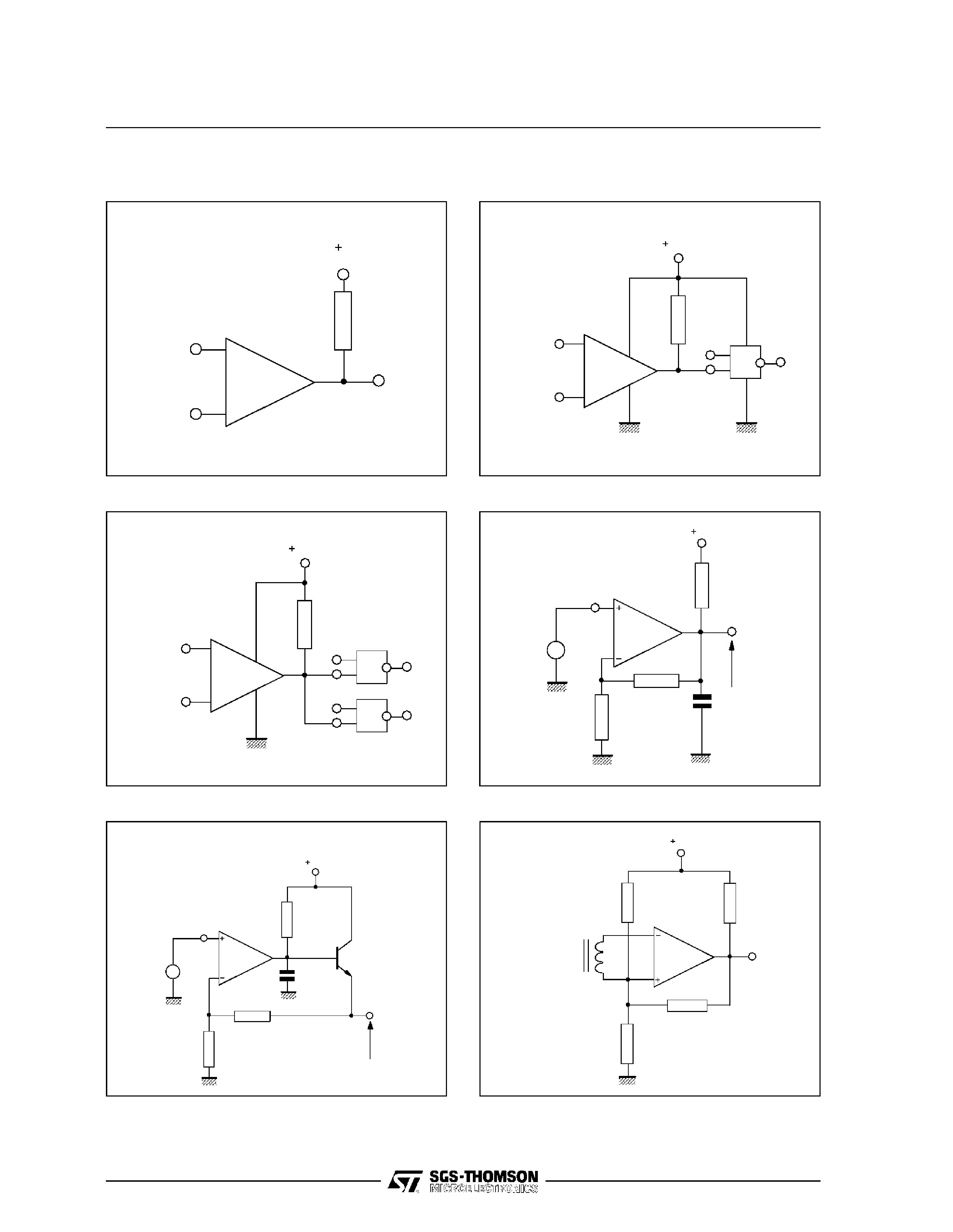
TYPICAL APPLICATIONS
BASIC COMPARATOR
5V
100k
+V
(r ef )
-V
(r ef )
1/2
LM193
&
193-09.EPS
DRIVING CMOS
5V
10k
+V
(ref)
-V
(ref)
1/2
LM193
&
&
193-10.EPS
DRIVING TTL
5V
15k
1/2
LM193
e o
0.5
µF
100k
e I
1k
A = 100
V
~
193-11.EPS
LOW FREQUENCY OP AMP
5V
15k
1/2
LM193
eo
0.5
µF
100k
e
I
1k
A = 100
V
~
2N 2222
(e = 0V for e = 0V)
I
o
193-12.EPS
LOW FREQUENCY OP AMP
5V
10k
1/2
LM193
eo
20M
10k
3k
Magnetic pick-up
193-13.EPS
TRANSDUCER AMPLIFIER
LM193 - LM293 - LM393
5/9