(without price)
JULY 1997
DP-8000

CONTENTS
1. SPECIFICATIONS ................................................................................................................................ 1
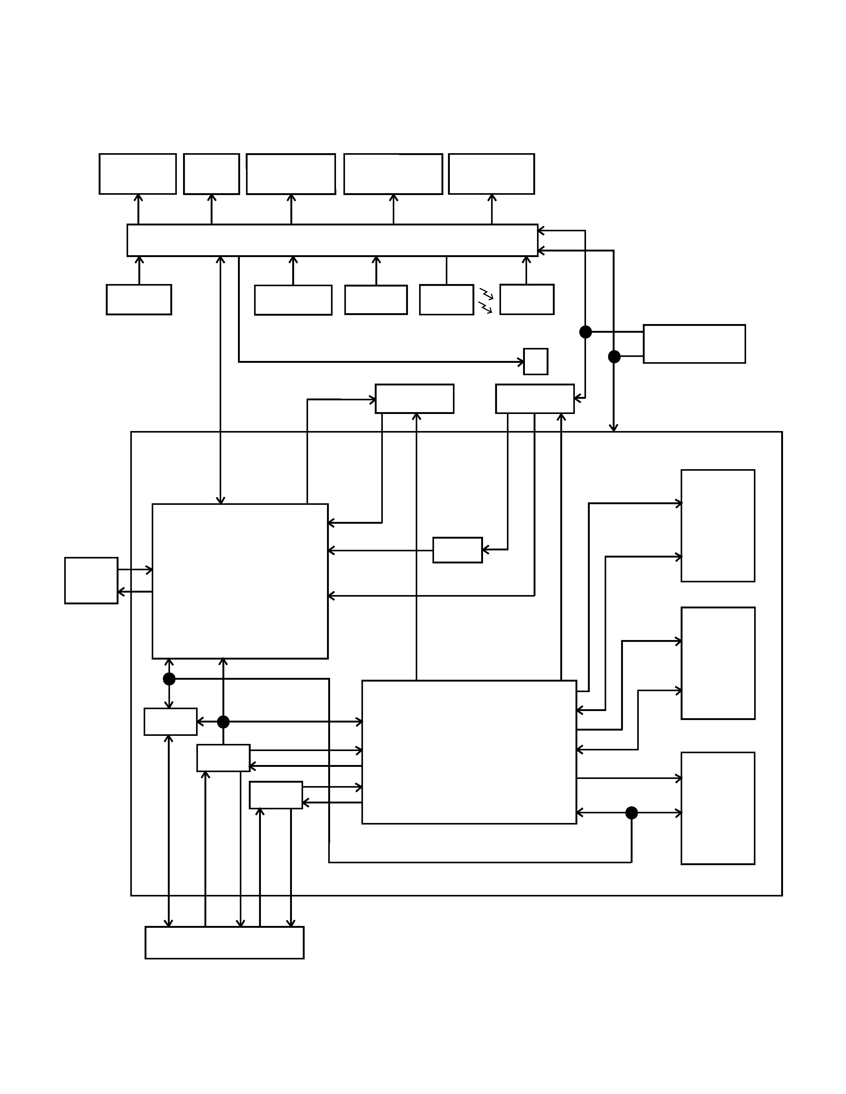
2. BLOCK DIAGRAM ............................................................................................................................... 2
3. LSI PIN FUNCTION .............................................................................................................................. 3
4. DISASSEMBLY
4-1. Removing printer ass'y. ............................................................................................................ 7
4-2. Removing side frame L ass'y. ................................................................................................... 7
4-3. Removing side frame R ass'y. .................................................................................................. 7
4-4. Removing fan and DC motor for head cam. ............................................................................ 7
5. REPLACEMENT AND ADJUSTMENT OF HEAD
5-1. Removing head holder ass'y. ................................................................................................... 9
5-2. Installation and adjustment of head ...................................................................................... 10
6. ADJUSTMENT OF PRINT DENSITY ................................................................................................. 12
7. DIAGNOSTIC PROGRAM .................................................................................................................. 13
8. PRINT PROCESS ............................................................................................................................... 17
9. HEAD SENSING MARK AND POSITION OF HEAD ......................................................................... 20
10. PRINT SENSOR ................................................................................................................................. 21
11. ERROR MESSAGE ............................................................................................................................ 22
12. PARTS LIST ....................................................................................................................................... 23
13. EXPLODED VIEW .............................................................................................................................. 26
14. SCHEMATIC DIAGRAMS
14-1. Wiring diagram . ..................................................................................................................... 28
14-2. Block diagram PCB Z566-1. ..................................................................................................29
14-3. Relay block PCB Z566-2. ....................................................................................................... 30
14-4. Power supply block PCB Z566-S1. ....................................................................................... 31
14-5. Key block PCB Z566-E4 ........................................................................................................ 32
14-6. Ribbon color sensor PCB Z566-3 ......................................................................................... 33
14-7. Paper jam sensor PCB Z566-4 .............................................................................................. 33
14-8. Paper sensor 1 PCB Z566-5 ..................................................................................................33
14-9. Head cam sensor PCB Z566-6 .............................................................................................. 33
14-10. Cassette SW PCB Z566-7 ....................................................................................................34
14-11. Back cover SW PCB Z566-8 ................................................................................................ 34
14-12. Transmit block PCB Z566-9 ................................................................................................ 34
14-13. Paper sensor 2 PCB Z566-10 .............................................................................................. 34
14-14. PC-Link block PCB Z566-11 ................................................................................................ 35

-- 1 --
1. Specifications
Printing System
Sublimation thermal line printer
Pixels
PC: 960
× 1920 dots (480 × 640 dots)
QV Digital Camera: 480
× 640 dots
Resolution
PC: 297
× 446 dpi (149 × 149 dpi)
QV Digital Camera: 149
× 149 dpi
Color
256 gradations,16.77 million colors
Paper Size
100
× 148 mm (3-15/16 × 5-13/16 inches) A6 size
Print Size
82
× 109 mm (3-1/4 × 4-15/16 inches)
Paper Feed
Manual
Input Terminals
DIGITAL terminal; Centronics standard bi-directional
parallel port
Power
AC adapter (AD-2418; Rated Input: 24 V)
Power Consumption
Approximately 53 W
Number of Buttons
7
Functions
Easy Printing; background, calendar, post card, mini label, illustration
printing directly from QV Digital Camera or personal computer
Maximum Dimensions
71.5 (H)
× 250 (W) × 317 (D) mm (12-13/16 H × 9-7/8 W × 12-1/2 D inches)
Weight
2.3 kg (5 lbs)
Operating Temperature
5
°C to 35 °C
Included Items
AC adapter (AD-2418); Communication Cable (SB-62), Ink Cartridge;
Special Paper, Printer Driver for Windows; User's Guide; Printer Drive
User's Guide; Printer Samples
OPTIONS
Paper Sets
· QV-101 Standard Paper Set
25 pieces of standard paper + one ink cartridge
· QV-102 Standard Paper (Postcard Type) Set
25 pieces of standard paper (postcards) + one ink cartridge
· QV-201 Sticker Paper Set
25 pieces of sticker paper + one ink cartridge
· QV-202 16-image Sticker Paper Set
25 pieces of 16-image sticker paper + one ink cartridge
-- 2 --
Steppin motor
for paper feeding
DC motor for
head up/down
Back case open
detection switch
PCB-Z566-2
Z566-S1 PCB
POWER SUPPLY
Ribon
rewinding
motor
Ribon cassette
detectection switch
UPD23C8000XGX-355
UPD424260LE-70-E2
ROM
D RAM
CPU
UPD70P3000GC-25
HD74LS
14FPTR
HD74LS
373FPEL
HD74LS
14FPTR
Z566-11 PCB
PC LINK BLOCK
TO PC
GATE ARRAY
UPD65643GD-032-5BD
M5M52780J-15-T1
PCB-Z566-7
PCB-Z566-8
HEAD.M1,
HEAD.M2
RBN.M+,
RBN.M
STP.MA STP.MB,
STP.MA- STP.MB-
RBN.M+,
RBN.M-
URA.F
Head cam
sensor
PCB-Z566-6
Fan
Printer Head
Z566-E4 PCB
KEY and LED
Ribbon color
sensor
Paper jam
sensor
Paper
sensor 1
PCB-Z566-3
PCB-Z566-4 PCB-Z566-5
PCB-Z566-10
Z566-9
Transmit
Block
To QV
S RAM
PCB-Z566-1
Paper
sensor 2
CAM.S1,
CAM.S2
RIBBON.S
PJAM.S
PAPER.S
24V
5V
KO0, KO1
KI0 ~ KI3
TA756393
TH
Temperature
sensor
RANK1 ~
RANK3
LED0 ~ LED3
HDADA1 ~
HDATA10,
HSTBB,
HLAT,
HCLK
PD0 ~
PD7
PSRTRBB
INITB,
SLCTINB
FAULT
AFXB
ACKB,
BUSY,
PE,
SELECT
CAD0 ~ CAD15 (I/O0 ~ I/O15)
A0 ~ A8, WE,
RAS, UCAS,
LCAS
AO ~ A14,
CE, OE, WE
D0 ~ D7
A0 ~ A18,
CE, OE, WE
O0 ~ O15
RX
TX
2. Block Diagram

-- 3 --
3. LSI Pin Function
(1) CPU (UPD703000GC)
Pin No.
Name
I/O
Function
1 ~ 5
A20 ~ A16
O
Address bus
6
GND
Ground terminal
7
VDD
VDD terminal
8 ~ 15
AD15 ~ AD8
I/O
Data bus
16
VDD
VDD terminal
17
GND
Ground terminal
18 ~ 25
AD7 ~ AD0
Data bus
26
GND
Ground terminal
27
VDD
VDD terminal
28
LBENB
Communication with gate array
29
UBENB
Communication with gate array
30
R/WB
Read/Write signal
31
DSTB
Data strobe signal
32
ASTB
Address strobe signal
33
P95
34
P96
35
P97
VP ON signal output terminal
36
WAITB
Wait signal
37
VDD
VDD terminal
38
GND
Ground terminal
39, 40
X2, X1
Clock pulse
41
CKSEL
Connected to ground
42
CVDD
Connected to VDD
43
CGND
Ground terminal
44
CLKOUT
O
Clock pulse to gate array
45
GND
Ground terminal
46
VDD
VDD terminal
47
P103
I
Detection of ribbon color
48 ~ 50
P102 ~ P100
I
Key scanning signal
51
RESETB
I
Reset signal
52
IC1
Connected to VDD
53
IC0
Connected to ground
54
MODE1
VDD terminal
55
MODE0
Connected to ground
56
VDD
Connected to VDD
57
GND
Ground terminal
58, 59
P10, P11
O
Key scanning signal
60
P12
SVCC signal output
61
P13
O
Output from temperature observation circuit
62
P14
I
Input from temperature observation circuit
63 ~ 65
P15 ~ P17
I
Setting for head rank
66
GND
Ground terminal
67
VDD
VDD terminal
68
P00
Fan drive signal
69
P01
Data for system ROM
70
P02
Data for system ROM
71
P03
Serial clock pulse for system ROM
72
P04
Chip enable signal for system ROM
73
P05
I
Detection of back case
74
P06
I
Detection of ribbon cassette
75
P07
Strobe signal from PC
76
VDD
VDD terminal