TDA7272A
HIGH PERFORMANCE MOTOR SPEED REGULATOR
TACHIMETRIC SPEED REGULATION WITH
NO NEED FOR AN EXTERNAL SPEED PICK-
UP
V/I SUPPLEMENTARY PREREGULATION
DIGITAL CONTROL OF DIRECTION AND
MOTOR STOP
SEPARATE SPEED ADJUSTMENT
5.5V TO 18V OPERATING SUPPLY VOLT-
AGE
1A PEAK OUTPUT CURRENT
OUTPUT CLAMP DIODES INCLUDED
SHORT CIRCUIT CURRENT PROTECTION
THERMAL SHUT DOWN WITH HYSTERESIS
DUMP PROTECTION (40V)
ESD PROTECTION
DESCRIPTION
TDA7272A are high performance motor speed
controller for small power DC motors as used in
cassette players.
Using the motor as a digital tachogenerator itself
the performance of true tacho controlled systems
is reached.
A dual loop control circuit provides long term sta-
bility and fast settling behaviour.
This is advanced information on a new product now in development or undergoing evaluation. Details are subject to change without notice.
June 1992
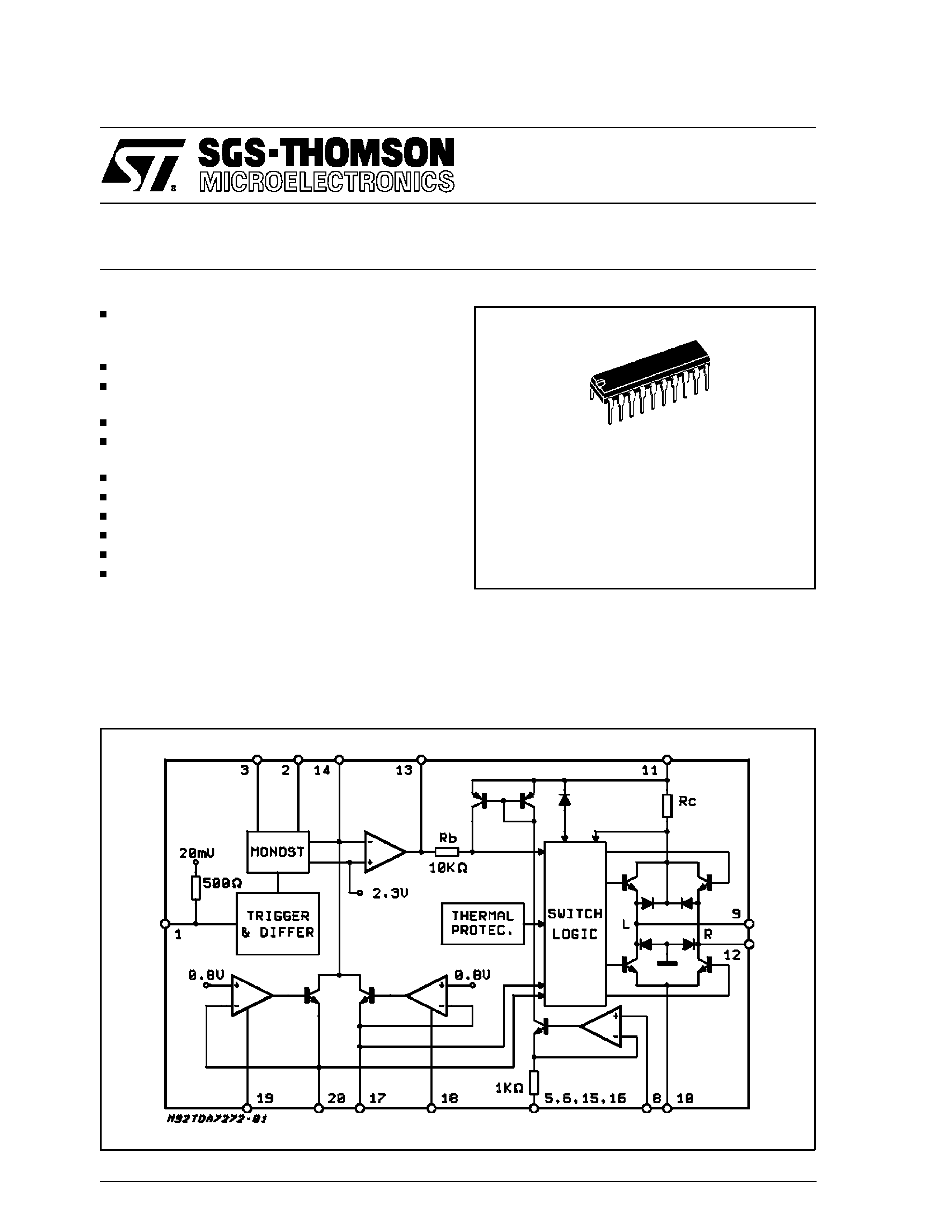
BLOCK DIAGRAM
Powerdip(16+2+2)
ORDERING NUMBER: TDA7272A
1/16
ABSOLUTE MAXIMUM RATINGS
Symbol
Parameter
Value
Unit
VS
DC Supply Voltage
24
V
VS
Dump Voltage (300ms)
40
V
IO
Output Current
Internally limited
Ptot
Power Dissipation at Tpins =90
°C
at Tamb =70
°C
4.3
1
W
W
Top
Operating Temperature Range
-40 to 85
°C
Tstg
Storage Temperature
-40 to 150
°C
THERMAL DATA
Symbol
Parameter
Value
Unit
Rth j-amb
Thermal Resistance Junction-ambient
max.
80
°C/W
Rth j-pins
Thermal Resistance Junction-pins
max.
14
°C/W
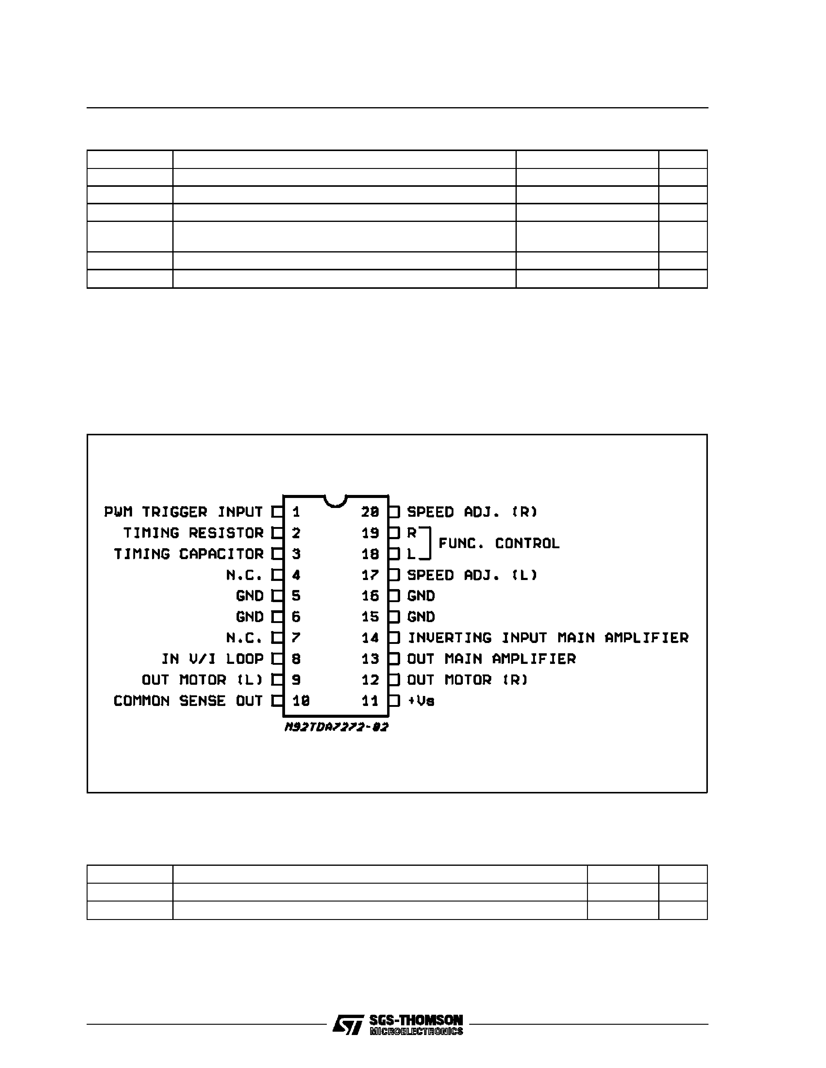
PIN CONNECTION (Top view)
TDA7272A
2/16
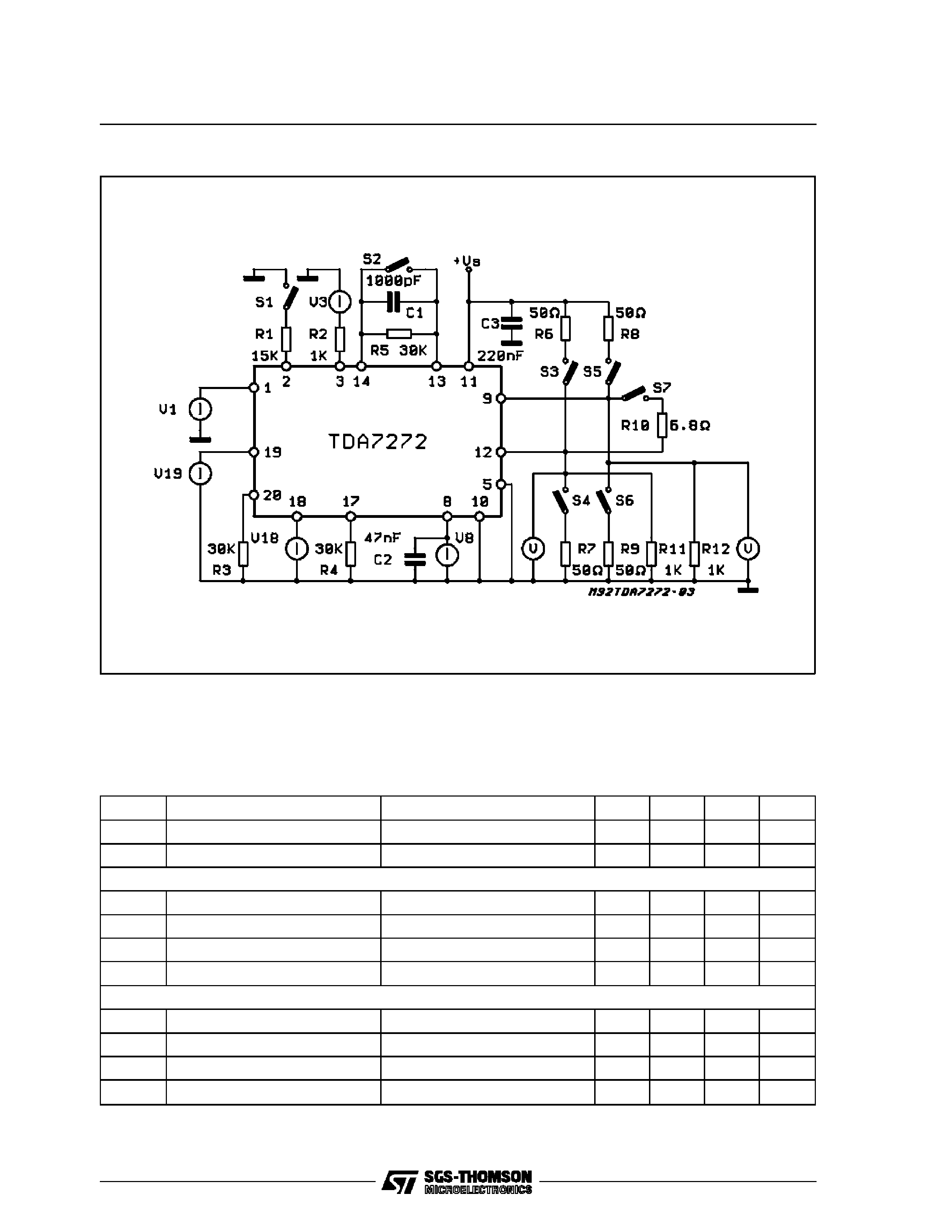
TEST CIRCUIT
ELCTRICAL CHARACTERISTICS (Tamb =25
°C; VS = 13.5V unless otherwise specified)
Symbol
Parameter
Test Conditions
Min.
Typ.
Max.
Unit
VS
Operating Supply Voltage
5.5
18
V
IS
Supply Current
No load
5
12
mA
OUTPUT STAGE
IO
Output Currente Pulse
1
A
IO
Output Currente Continuous
250
mA
V10,9,12
Voltage Drop
IO = 250mA
1.2
1.5
V
V11,9,12
Voltage Drop
IO = 250mA
1.7
2
V
MAIN AMPLIFIER
R14
Input Resistance
100
K
Ib
Bias Current
50
nA
VOFF
Offset Voltage
1
5
mV
VR
Reference Voltage
Internal at non inverting input
2.3
V
A
TDA7272A
3/16
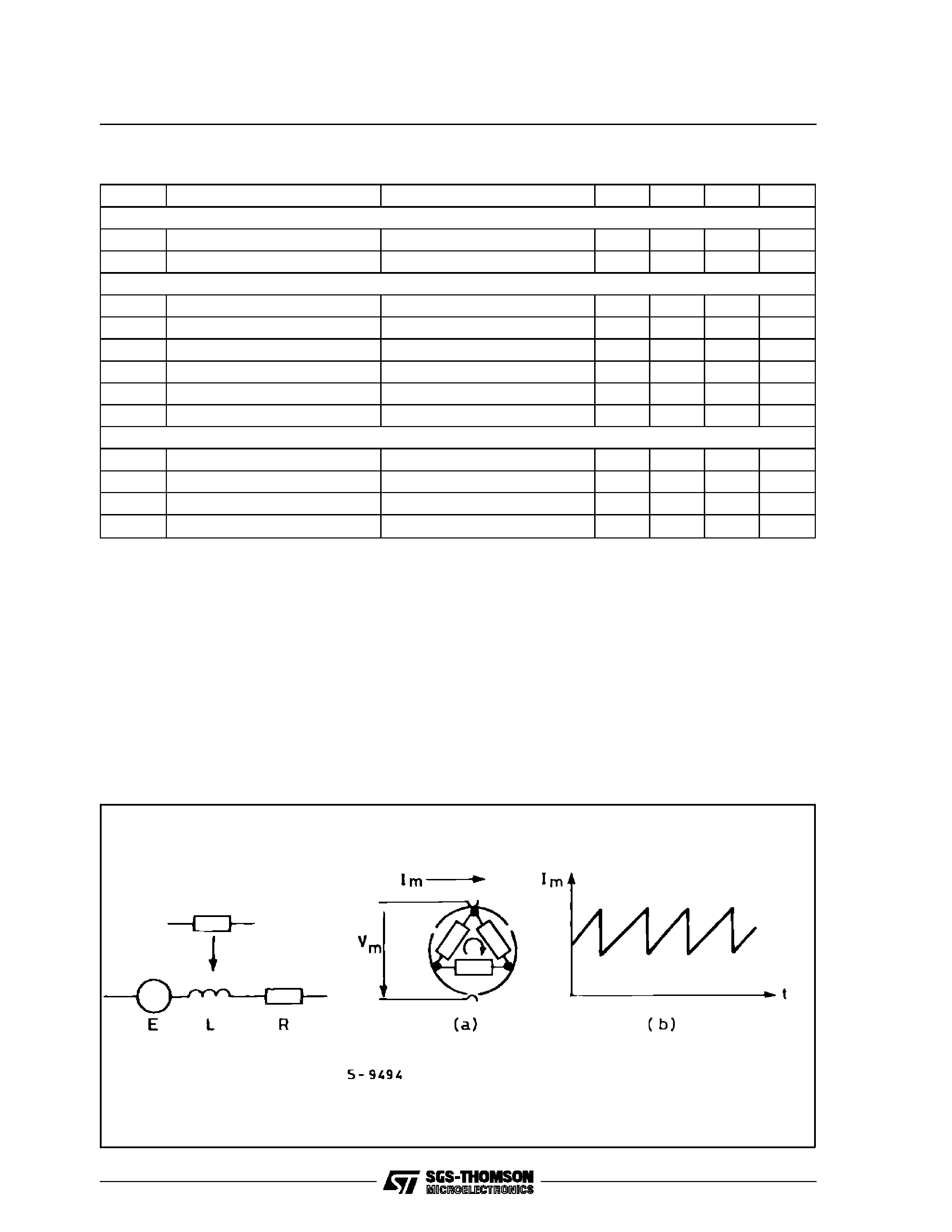
The TDA7272A novel applied solution is based
on a tachometer control system without using
such extra tachometer system. The information of
the actual motor speed is extracted from the mo-
tor itself. A DC motor with an odd number of poles
generates a motor current which contains a fixed
number of discontinuities within each rotation. (6
for the 3 pole motor example on fig. 1)
Deriving this inherent speed information from the
motor current, it can be used as a replacement of
a low resolution AC tachometer system. Because
the settling time of the control loop is limited on
principle by the resolution in time of the tachome-
ter, this control principle offers a poor reaction
time for motors with a low number of poles. The
realized circuit is extended by a second feed for-
ward loop in order to improve such system by a
fast auxiliary control path.
This additional path senses the mean output cur-
rent and varies the output voltage according to
the voltage drop across the inner motor resis-
tance. Apart from a current averaging filter, there
is no delay in such loop and a fast settling behav-
iour is reached in addition to the long term speed
motor accuracy.
ELECTRICAL CHARACTERISTICS (Continued)
Symbol
Parameter
Test Conditions
Min.
Typ.
Max.
Unit
CURRENT SENSE AMPLIFIER
R8
Input Resistance
100
K
GL
Loop Gain
9
TRIGGER AND MONOSTABLE STAGE
VIN1
Input Allowed Voltage
-0.7
3
V
RIN1
Input Resistance
500
VT Low
Trigger Level
0
V
VTB
Bias Voltage (pin 1)
15
20
25
mV
VTH
Trigger Histeresis
10
mV
V2 REF
Reference Voltage
750
800
850
mV
SPEED PROGRAMMING, DIRECTION CONTROL LOGIC AND CURRENT SOURCE PROGRAMMING
V18,19 Low
Input Low Level
0.7
V
V18,19 High
Input High Level
2
V
I18,19
Input Current
0 < V18,19 <VS
2
µA
V17,20 REF
Reference Voltage
735
800
865
mV
Figure 1: Equivalent of a 3 Pole DC Motor (a) and Typical motor Current Waveform (b).
TDA7272A
4/16
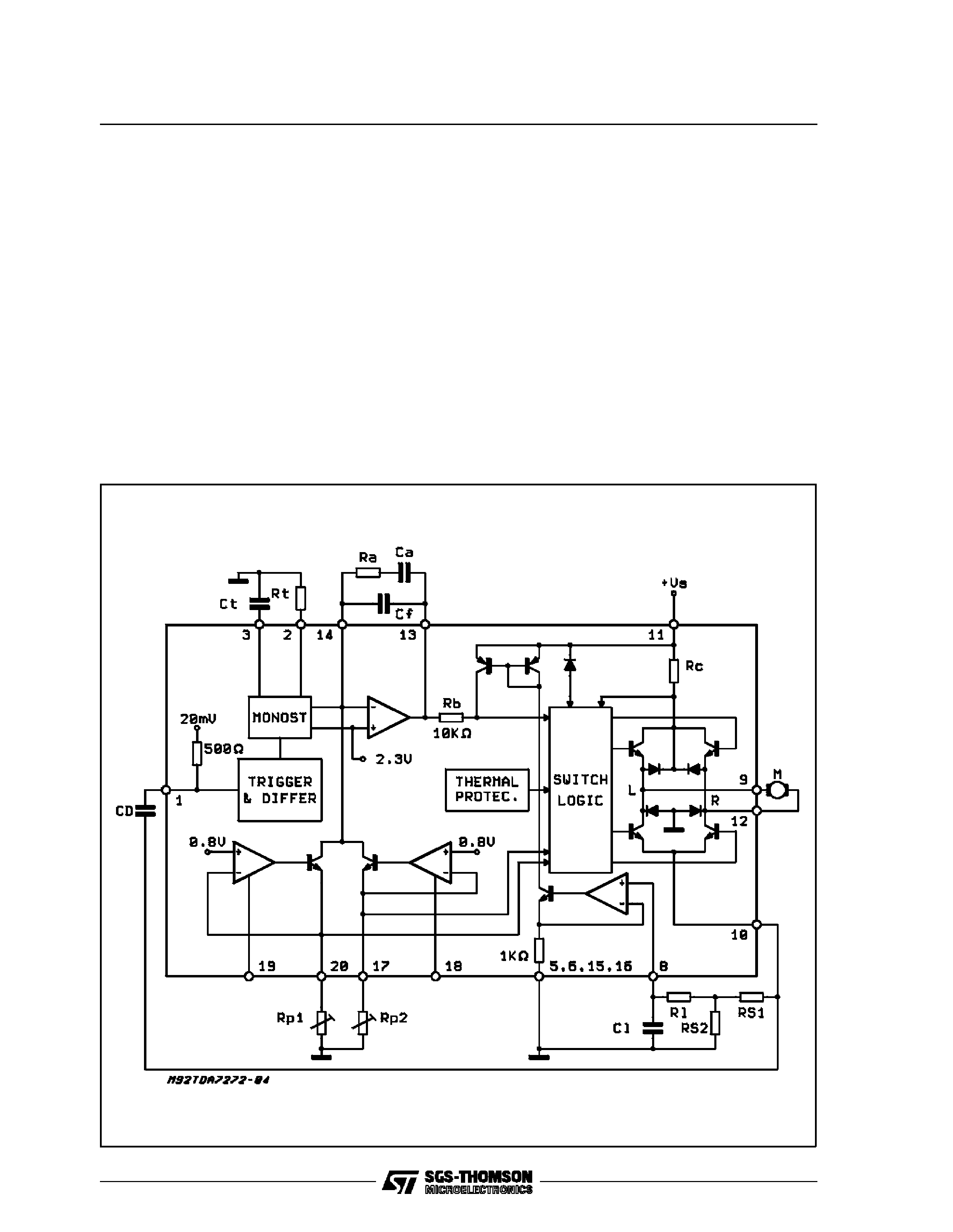
BLOCK DESCRIPTION
The principle structure of the element is shown in
fig. 2. As to be seen, the motor speed information
is derived from the motor current sense drop
across the resistors RS ; capacitor CD together
with the input impedance of 500
at pin 1 real-
izes a high pass filter.
This pin is internally biased at 20 mV, each nega-
tive zero transition switches the input comparator.
A 10 mV hysteresis improves the noise immunity.
The trigger circuit is followed by an internal delay
time differentiator.
Thus, the system becomes widely independent of
the applied waveform at pin 1, the differentiator
triggers a monostable circuit which provides a
constant current duration. Both, output current
magnitude and duration T, are adjustable by ex-
ternal elements CT and RT.
The monostable is retriggerable ; this function
prevents the system from fault stabilization at
higher harmonics of the nominal frequency.
The speed programming current is generated by
two separate external adjustable current sources.
A corresponding digital input signal enables each
current source for left or right rotation direction.
Resistor RP1 and RP2 define the speed, the logi-
cal inputs are at pin 18 and 19.
At the inverting input (pin 14) of the main amplifier
the reference current is compared with the pulsed
monostable output current.
For the correct motor speed, the reference cur-
rent matches the mean value of the pulsed
monostable current. In this condition the charge
of the feedback capacitor becomes constant.
Figure 2: Application Circuit.
TDA7272A
5/16