L6374
INDUSTRIAL QUAD LINE DRIVER
ADVANCE DATA
FOUR INDEPENDENT LINE DRIVERS WITH
100 mA UP TO 35V OUTPUTS
INPUT SIGNALS BETWEEN -7V AND +35V,
WITH PRESETTABLE THRESHOLD
PUSH-PULL OUTPUTS WITH THREE STATE
CONTROL AND TRUE ZERO CURRENT BE-
TWEEN VS AND GROUND
CURRENT LIMITING ON EACH OUTPUT EF-
FECTIVE IN THE FULL "GROUND TO VS"
OUTPUT VOLTAGE RANGE
OUTPUT VOLTAGE CLAMP TO VS AND TO
GROUND
OVERTEMPERATURE
AND
UNDERVOL-
TAGE PROTECTIONS
DIAGNOSTIC FOR OVERTEMPERATURE,
UNDERVOLTAGE AND OVERCURRENT
PRESETTABLE
DELAY
FOR
OVERCUR-
RENT DIAGNOSTIC
HIGH SPEED OPERATION: UP TO 300kHz
WITH 35V SWING
DESCRIPTION
The L6374 is especially designed to be used as a
line driver in industrial control systems based on
the 24V signal levels (IEC1131, 24VDC).
This is advanced information on a new product now in development or undergoing evaluation. Details are subject to change without notice.
December 1994
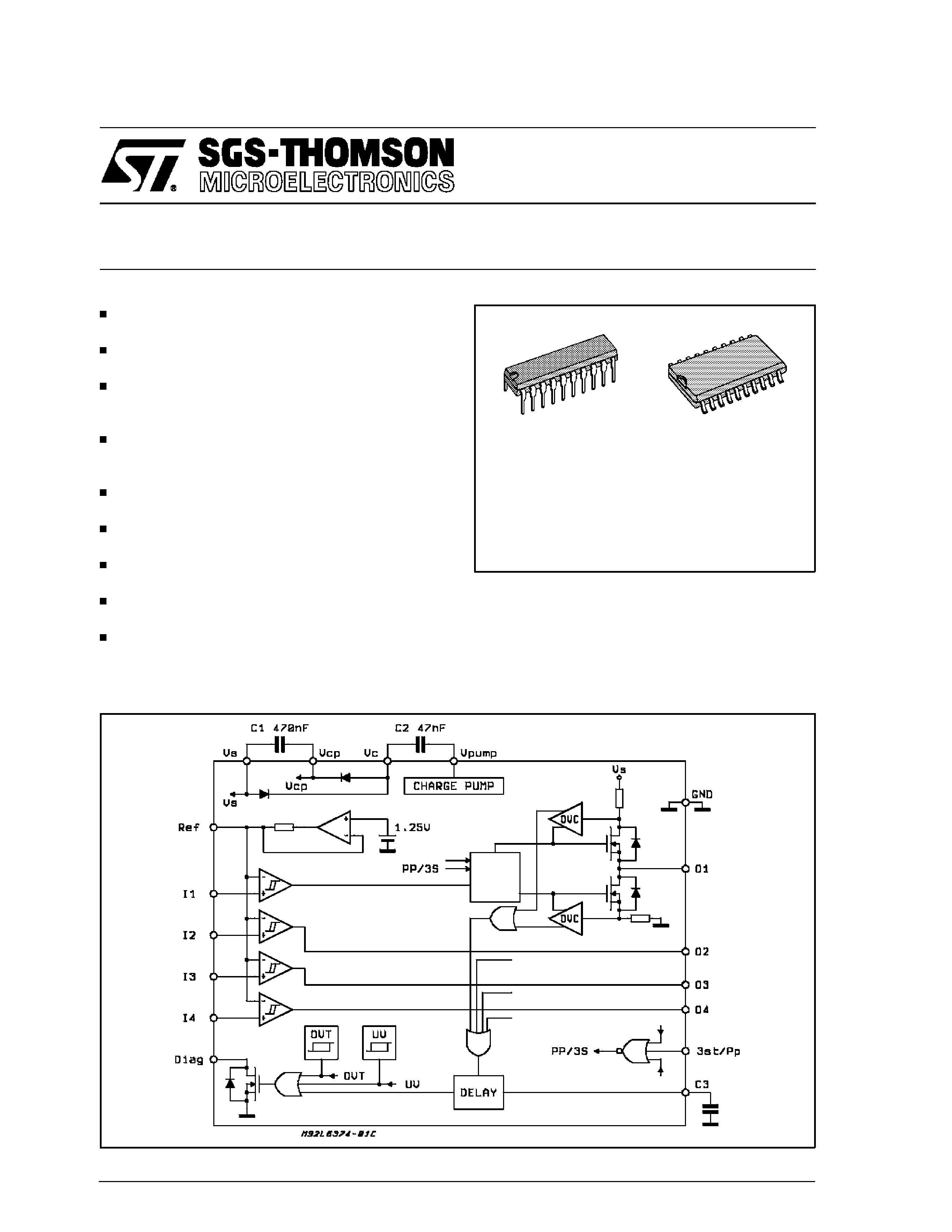
BLOCK DIAGRAM
ORDERING NUMBER: L6374DP (POWERDIP 16+2+2)
L6374FP (SO 16+2+2)
POWERDIP 16+2+2
SO 16+2+2
1/13
ABSOLUTE MAXIMUM RATINGS
Symbol
Pin
Parameter
Value
Unit
VS
1
Supply Voltage (tW < 10ms)
50
V
Supply Voltage (DC)
40
V
Vilog
12, 13
Logic Input Voltage (DC)
-0.3 to 7
V
Iilog
Logic Input forced current, per pin
±1mA
Ii
7, 8,
9, 10
Channel Input Current (forced)
±2mA
Vi
Channel Input Voltage
- 7 to 35
V
Iout
3, 4,
17, 18
Output Current (forced, apart from inductive load)
±100
mA
Output Current (forced, apart from inductive load)
same tW < 10ms
±1A
Vout
Output Voltage (forced, not resulting from an inductive
kick)
-0.3 to VS +0.3
V
Iset
11
Setting pin forced current
±1mA
Vset
Setting pin forced voltage
-0.3 to 5
V
Vdiag
14
External voltage
-0.3 to 35
V
Idiag
Externally forced current
-10 to 10
mA
VC3
13
Voltage on the delay capacitor, externally forced
-0.3 to 4.5
V
Top
Ambient temperature, operating range
-25 to 85
°C
Tj
Junction temperature, operating range (see
Overtemperature Protection)
-25 to 125
°C
Tstg
Storage temperature
-55 to 150
°C
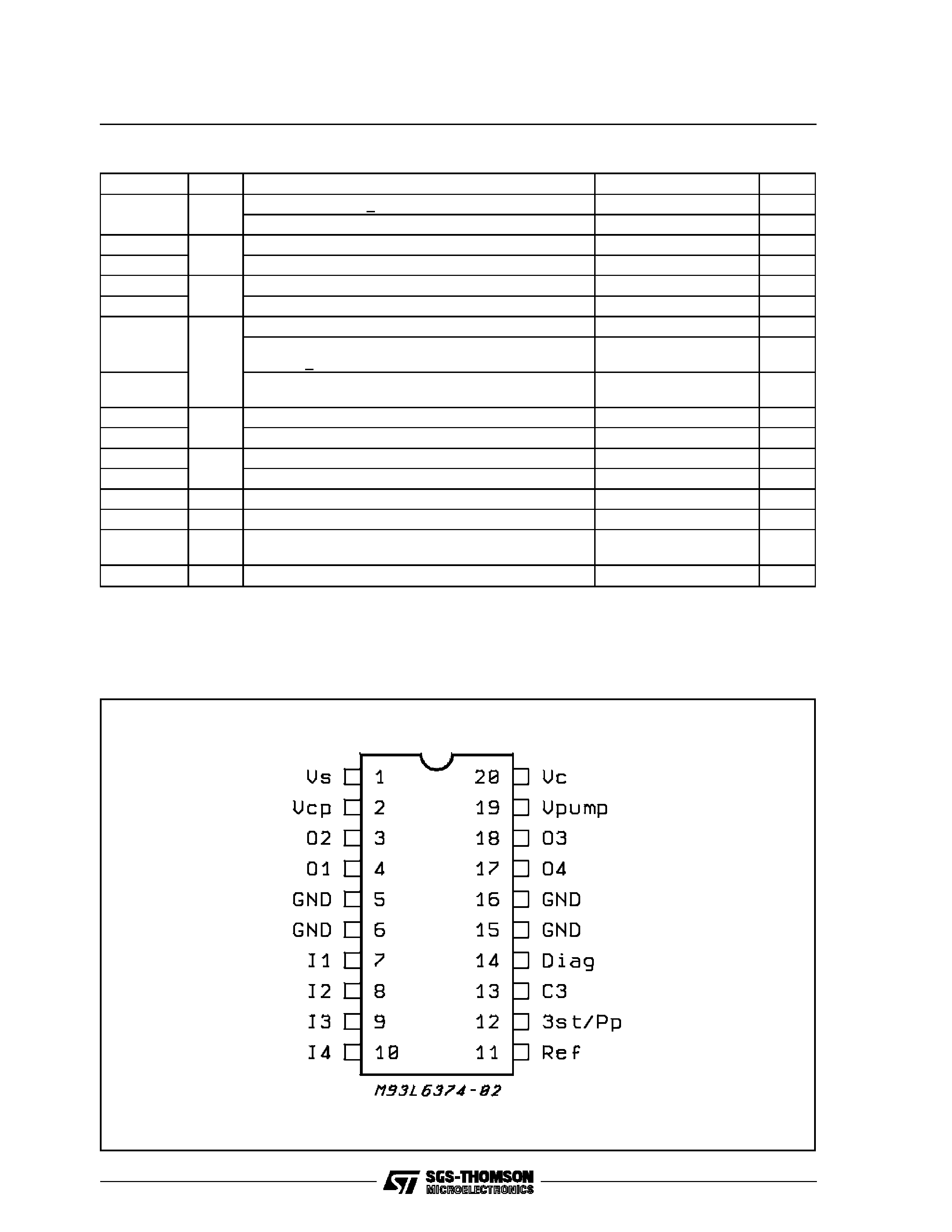
PIN CONNECTION (Top view)
L6374
2/13
ELECTRICAL CHARACTERISTICS (VS = 24V; Tj = -25 to 125
°C; unless otherwise specified.)
DC OPERATION
Symbol
Pin
Parameter
Test Condition
Min.
Typ.
Max.
Unit
VS
1
Supply Voltage
10.8
35
V
Vsh
UV UpperThreshold
9
10.8
V
Hys1
UV Hysteresis
250
450
650
mV
Iqsc
Quiescent Current
Outputs Open
3
5
mA
Vref
11
Input Comparators Reference
Voltage
Reference pin Floating
1.05
1.25
1.35
V
Iref
Sink/Source Current on
Reference Pin
Vref = 0V
-30
-20
-10
µA
Vref =5V
10
20
30
µA
Vth
7, 8,
9, 10
Comparator Threshold with
External Bias
VS = 9 to 12V
-0.2
2.0
V
VS = 12 to 35V
-0.2
5.0
V
Vil
Input Low Level
VREF Externally Biased
-7
VREF
-0.2
V
Pin VREF Floating
-7
0.8
V
Vih
Input High Level
VREF Externally Biased
VREF
+0.2
35
V
Pin VREF Floating
2
35
V
Vi
Input Voltage (Operative Range)
-7
35
V
Ibias
Input Bias Current
0 < Vi <VS
-1
1
µA
Vi = -7V
-1
-0.5
-0.1
mA
Hys2
Input Comparators Hysteresis
See Analog Inputs Sections
100
200
350
mV
Th
OVT Upper Threshold
170
°C
HT
OVT Hysteresis
20
°C
Isc
3, 4,
17, 18
Current Limit
Vi =-7 to VS;Vout = 0 to VS;
110
200
300
mA
Von
Internal Voltage Drop @ Rated
Current
Iout =
±100mA; Sourced @ High
Output, Sunk @ Low Output
Tj = 125
°C
400
600
mV
Same, Tj =25
°C
250
400
mV
Ilkg
Output 3-State Leakage Current
Vout = 0 to VS
-25
25
µA
Vin
12
Push-Pull Mode Request
-0.2
0.8
V
3-State Mode Request
2
5.5
V
Iin
Input Current
Vi =0V
10
25
µA
Idlkg
14
Diagnostic Output Leakage
Diagnostic Off; Vdiag = 24V
5
µA
Vdiag
Diagnostic Output Voltage Drop
Idiag =5mA
200
500
mV
AC OPERATION (VS = 10.8 to 35V; Tj = -25 to 125
°C; Iout = 100mA; unless otherwise specified; see
switching waveforms diagrams)
Symbol
Pin
Parameter
Test Condition
Min.
Typ.
Max.
Unit
tdr
7to 4
8to 3
9 to18
10to17
Delay Time on Rising Edge
Rl to ground
1000
1500
ns
Rl to VS
500
1000
ns
tdf
Delay Time on Falling Edge
Rl to ground
500
1000
ns
Rl to VS
1000
1500
ns
tr
3, 4,
17, 18
Rise Time
Rl to ground
120
250
ns
Rl to VS
120
250
ns
tf
Fall Time
Rl to ground
150
300
ns
Rl to VS
150
300
ns
L6374
3/13
THERMAL CHARACTERISTICS
Rth j-pins
POWERDIP. The thermal resistance is referred
to the thermal path from the dissipating region
on the top surface of the silicon chip, to the
points along the four central pins of the pack-
age, at a distance of 1.5 mm away from the
stand-offs.
SO. Similarly, the reference point is the knee
on the four central pins, where the pins are up-
wardly bent and the soldering joint with the
PCB footprint can be made.
Rth j-amb1
If a dissipating surface, thick at least 35
µm,
and with a surface similar or bigger than the
one shown, is created making use of the
printed circuit.
Such heatsinking surface is considered on the
bottom side of an horizontal PCB (worst case).
Rth j-amb2
If the power dissipating pins (the four central
ones), as well as the others, have a minimum
thermal connection with the external world
(very thin strips only) so that the dissipation
takes place through still air and through the
PCB itself.
It is the same situation of point above, without
any heatsinking surface created on purpose on
the board.
Additional data for the PowerDip package can be
found in:
Application Note 9030:
Thermal Characteristics of the PowerDip
20,24 Packages Soldered on 1,2,3 oz.
Copper PCB
THERMAL DATA
Symbol
Parameter
DIP20
SO20
Unit
Rth j-pin
Thermal Resistance, Junction to Pin
12
17
°C/W
Rth j-amb1
Thermal Resistance, Junction to Ambient (see Thermal
Characteristics)
40
65
°C/W
Rth j-amb2
Thermal Resistance, Junction to Ambient (see Thermal
Characteristics)
50
80
°C/W
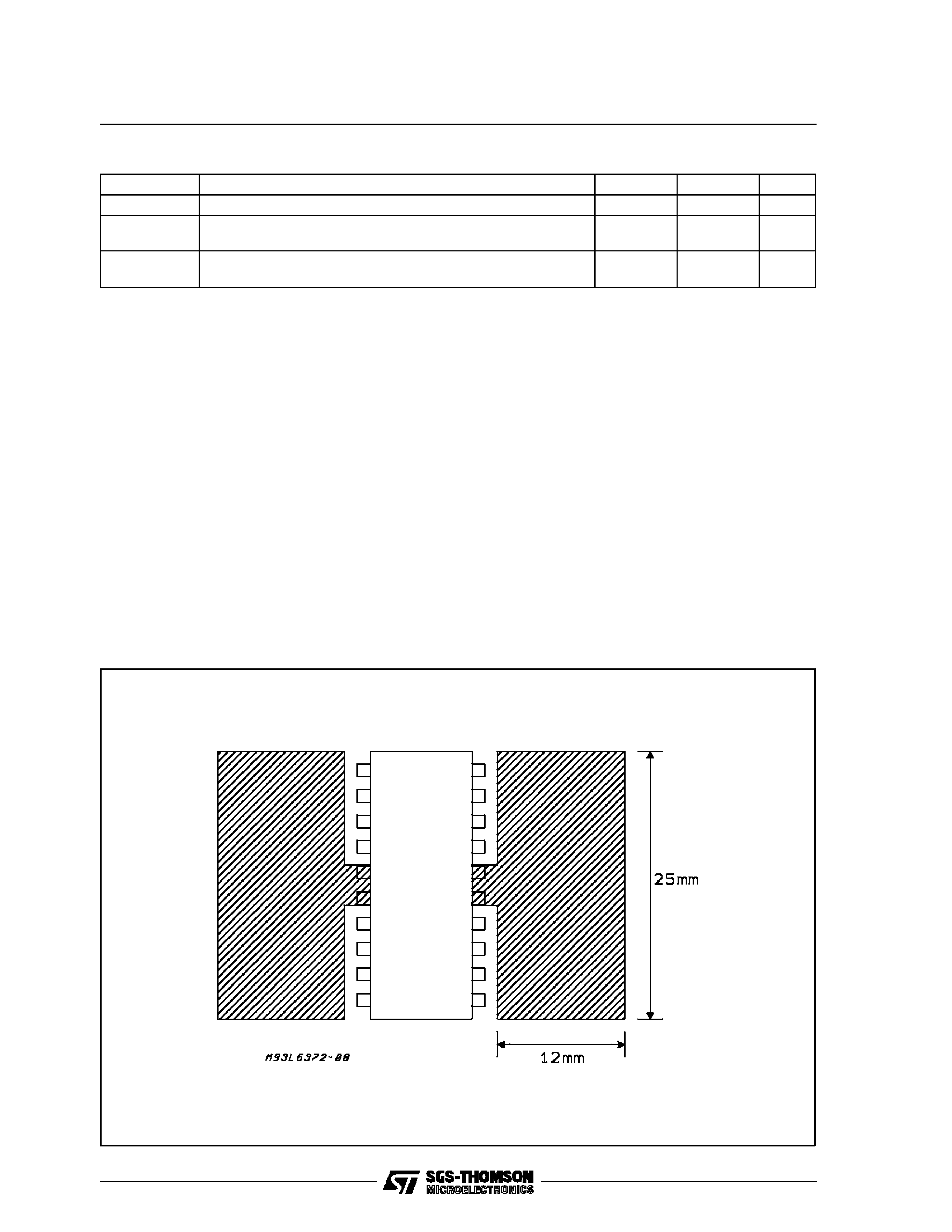
Figure 1: Printed Heatsink
L6374
4/13
OVERTEMPERATURE PROTECTION (OVT)
If the chip temperature exceeds Th (measured in
a central position in the chip) the chip deactivates
itself.
The following actions are taken:
- all the output stages are forced in the "three
state" condition, i.e. are disconnected from
the output pins; only the clamping diodes at
the outputs remain active;
- the signal Diag is activated (active low).
Normal operation is resumed as soon as (typically
after some seconds) the chip temperature moni-
tored goes back below Th -HT.
The different upper and lower thresholds with
hysteretic behavior, assure that no intermittent
conditions can be generated.
UNDERVOLTAGE PROTECTION (UV)
The supply voltage is expected to range from 11V
to 35V, even if its reference value is considered to
be 24V.
In this range the L6374 operates correctly.
Below 10.8V the overall system has to be consid-
ered not reliable.
Consequently the supply voltage is monitored
continuously and a signal, called UV, is internally
generated and used.
The signal is "on" as long as the supply voltage
does not reach the upper internal threshold of the
Vs comparator (called Vsh). The UV signal disap-
pears above Vsh.
Once the UV signal has been removed, the sup-
ply voltage must decrease below the lower
threshold (i.e. below Vsh -Hys1) before it is turned
on again.
The hysteresis Hys1 is provided to prevent inter-
mittent operation of the device at low supply volt-
ages that may have a superimposed ripple
around the average value.
The UV signal inhibits the outputs, putting them in
three-state, but has no effect on the creation of
the reference voltages for the internal compara-
tors, nor on the continuous operation of the
charge-pump circuits.
DIAGNOSTIC LOGIC
The situations that are monitored and signalled
with the Diag output pin are:
- current limit (OVC) in action; there are 8 indi-
vidual current limiting circuits, two per each
output, i.e. one per every output transistor;
they limit the current that can be either sour-
ced or sunk from each output, to a typical
value of 150mA, equal for all of them;
- undervoltage protection (UV);
- overtemperature protection (OVP);
The diagnostic signal is transmitted via an open
drain output (for ease of wired-or connection of
several such signals) and a low level represents
the presence of at least one of the monitored con-
ditions, mentioned above.
PROGRAMMABLE DELAY
The current limiting circuits can be requested to
perform even in absence of a real fault condition,
for a short period, if the load is of capacitive na-
ture or if it is a filament lamp (that exhibits a very
low resistance during the initial heating phase).
To avoid the forwarding of misleading, short diag-
nostic pulses in coincidence with the intervention
of the current limiting circuits when operating on
capacitive loads, a delay of about 5
µs is inserted
on the signal path, between the "OR" of the cur-
rent limit signals and its use as external diagnostic.
It takes about 1
µs to charge (or discharge) by
24V a capacitor of 5nF with a current of 120mA .
To implement longer delays (from the intervention
of one of the current limiting circuits to the activa-
tion of the diagnostic) an external capacitor can
be connected between pin C3 and ground (pin C3
is otherwise left open).
The delay shall then be determined by the ratio of
about 10 pF/
µs, using the value of the capaci-
tance connected to the pin.
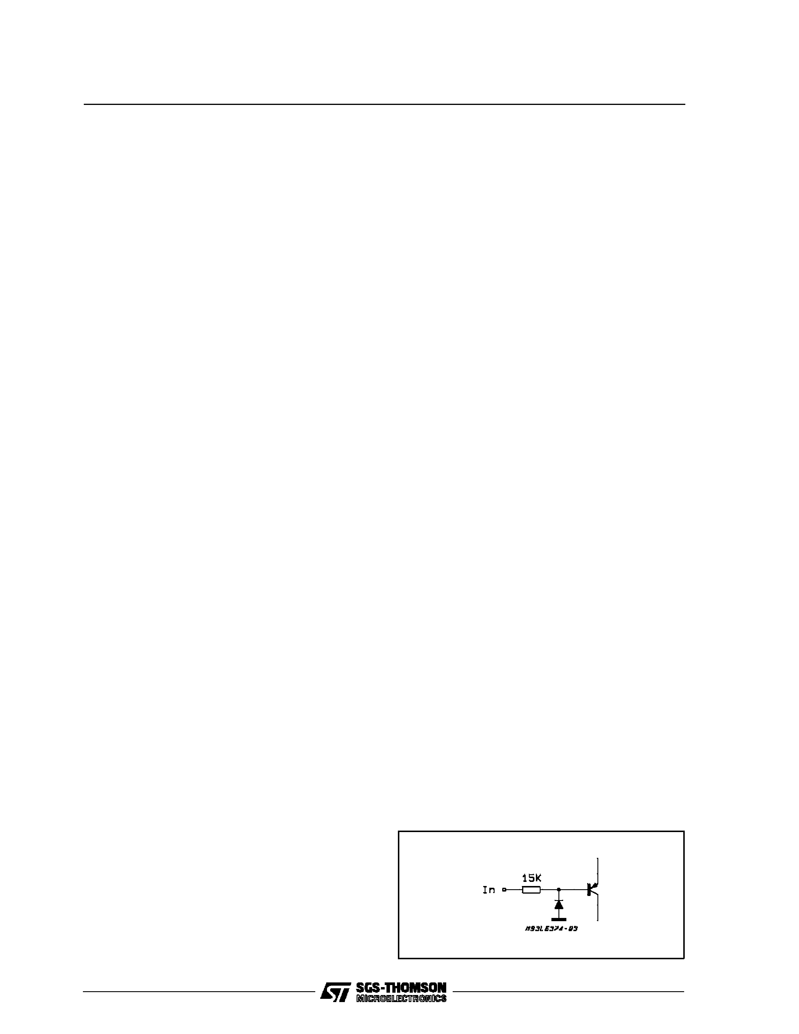
ANALOG INPUTS (I1,I2,I3,I4)
The input stage of each channel is a high im-
pedence comparator with
built-in
hysteresis
(200mV) for high noise immunity. Each compara-
tor has one input connected to all the others and
tied to a common pin Ref (Pin 11). If this pin is left
floating an internal precise band gap voltage ref-
erence (1.25V) is applied, otherwise these inputs
can be externally programmed by connecting an
external voltage source (from 0 to 5V) and the
current on this pin is internally limited to
±20µA.
The other input pin of each comparator can swing
from -7 to 35V.
For this reason it has been implemented the
structure shown in Figure 2 and the device can
also be used as line receiver.
When the input voltage is negative, the current is
internally limited by a 15k
resistor as shown in
Figure 2. High and low input thresholds can be
obtained by adding and subtracting half of the
hysteresis to the voltage of pin Ref (see Figure 3).
Figure 2: Equivalent input circuit
L6374
5/13