SERVICE MANUAL
DA
TA
BASIC DVD MECHANISM : DV21
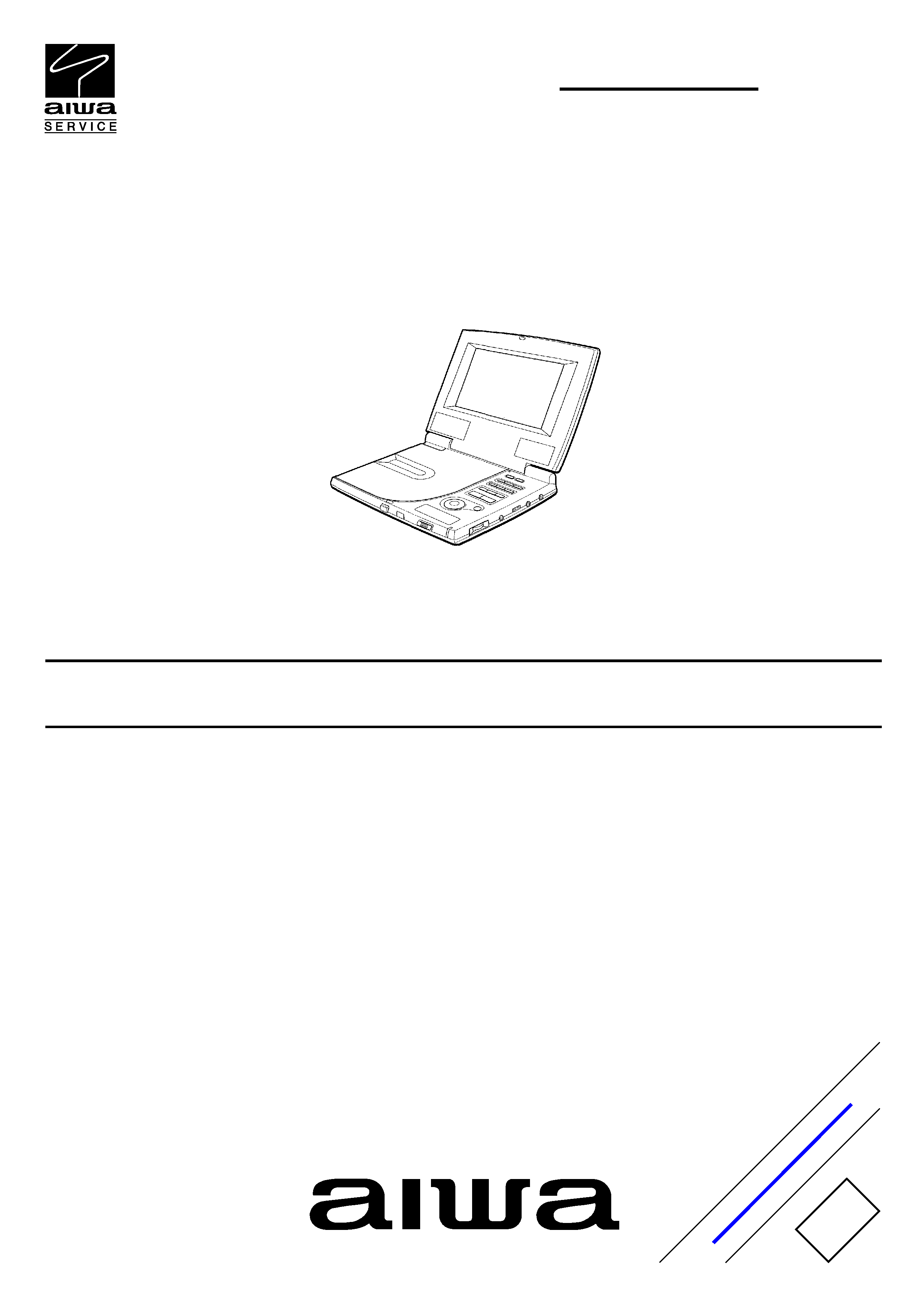
XD-DW5
S/M Code No. 09-01A-359-1R1
AHK(S)
REVISION
This Service Manual is the "Revision Publishing" and replaces "Simple Manual"
(S/M Code No. 09-01A-359-1T1).
DVD PLAYER
SIMPLE-2
Apar t ofcontentsisadequate.
Re-issuing is under r equest.

-2-
TABLE OF CONTENTS
SPECIFICATIONS .............................................................................................................................................. 3
ACCESSORIES/PACKAGE LIST-1/1 ................................................................................................................. 4
PROTECTION OF EYES FROM LASER BEAM DURING SERVICING ............................................................ 5
Precaution to replace Optical block ..................................................................................................................... 6
DISASSEMBLY INSTRUCTIONS .................................................................................................................. 7-16
ELECTRICAL MAIN PARTS LIST ............................................................................................................... 17-22
TRANSISTOR ILLUSTRATION-1/1 .................................................................................................................. 23
FL (AHU-1) GRID ASSIGNMENT/ANODE CONNECTION-1/1 ........................................................................ 24
BLOCK DIAGRAM-1/4 (FRONT END BLOCK) ................................................................................................ 25
BLOCK DIAGRAM-2/4 (BACK END BLOCK) ................................................................................................... 26
BLOCK DIAGRAM-3/4 (POWER BLOCK) ........................................................................................................ 27
BLOCK DIAGRAM-4/4 (TFT BLOCK) ............................................................................................................... 28
WIRING-1/15 (MAIN: COMPONENT SIDE) ..................................................................................................... 29
WIRING-2/15 (MAIN: 2nd LAYER) ................................................................................................................... 30
WIRING-3/15 (MAIN: 3rd LAYER) .................................................................................................................... 31
WIRING-4/15 (MAIN: 4th LAYER) .................................................................................................................... 32
WIRING-5/15 (MAIN: 5th LAYER) .................................................................................................................... 33
WIRING-6/15 (MAIN: CONDUCTOR SIDE) ..................................................................................................... 34
SCHEMATIC DIAGRAM-1/10 (MAIN 1/8) ......................................................................................................... 35
SCHEMATIC DIAGRAM-2/10 (MAIN 2/8) ......................................................................................................... 36
SCHEMATIC DIAGRAM-3/10 (MAIN 3/8) ......................................................................................................... 37
SCHEMATIC DIAGRAM-4/10 (MAIN 4/8) ......................................................................................................... 38
SCHEMATIC DIAGRAM-5/10 (MAIN5/8) .......................................................................................................... 39
SCHEMATIC DIAGRAM-6/10 (MAIN6/8) .......................................................................................................... 40
SCHEMATIC DIAGRAM-7/10 (MAIN 7/8) ......................................................................................................... 41
SCHEMATIC DIAGRAM-8/10 (MAIN 8/8) ......................................................................................................... 42
WIRING-7/15 (FRONT: COMPONENT SIDE) .................................................................................................. 43
WIRING-8/15 (FRONT: 2nd LAYER) ................................................................................................................ 44
WIRING-9/15 (FRONT: 3rd LAYER) ................................................................................................................. 45
WIRING-10/15 (FRONT: 4th LAYER) ............................................................................................................... 46
WIRING-11/15 (FRONT: 5th LAYER) ............................................................................................................... 47
WIRING-12/15 (FRONT: CONDUCTOR SIDE) ................................................................................................ 48
SCHEMATIC DIAGRAM-9/10 (FRONT) ........................................................................................................... 49
WIRING-13/15 (TFT: COMPONENT, CONDUCTOR SIDE) ............................................................................ 50
WIRING-14/15 (TFT: 2nd, 3rd LAYER) ............................................................................................................. 51
WIRING-15/15 (TFT: 4th, 5th LAYER) .............................................................................................................. 52
SCHEMATIC DIAGRAM-10/10 (TFT) ............................................................................................................... 53
VOLTAGE INFORMATION .......................................................................................................................... 54-57
WAVE FORM ............................................................................................................................................... 58-62
ELECTRICAL ADJUSTMENT ...................................................................................................................... 63-68
INITIALIZE MODE-1/1 ...................................................................................................................................... 69
IC BLOCK DIAGRAM ................................................................................................................................... 70-76
IC DESCRIPTION ........................................................................................................................................ 77-99
MECHANICAL EXPLODED VIEW-1/1 ............................................................................................................ 100
MECHANICAL PARTS LIST-1/1 ............................................................................................................. 101, 102
-3-
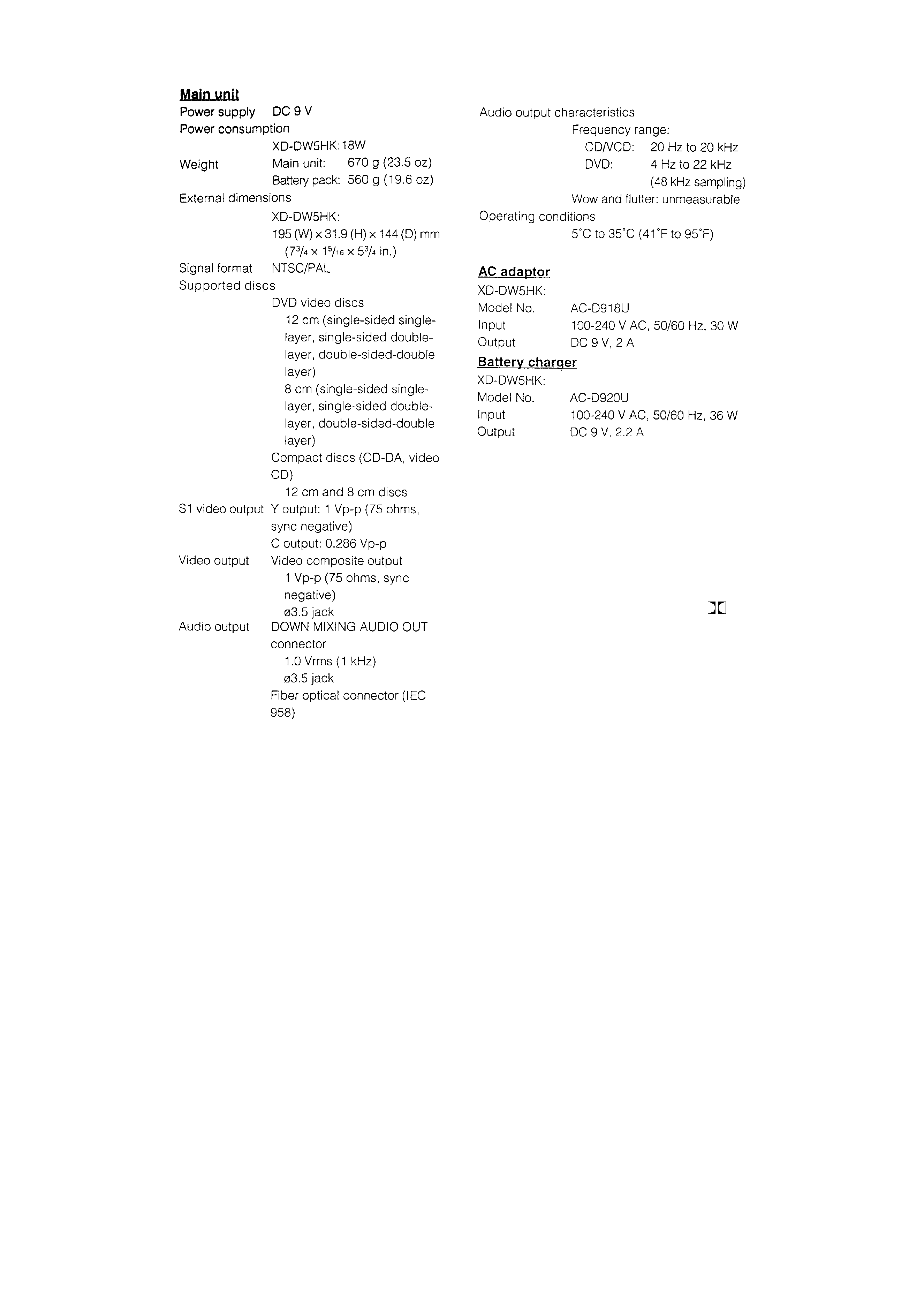
SPECIFICATIONS
· Design and specifications are subject to change without
notice.
· Dolby noise reduction manufactured under license from
Dolby Laboratories Licensing Corporation.
"DOLBY" and the double-D symbol
are trademarks
of Dolby Laboratories Licensing Corporation.
· Manufactured under license from Digital Theater Systems, Inc.
US Pat. No.5,451,942 and other worldwide patents Issued and
pending. "D T S" and "D T S Digital Surround" are trade marks of
Digital Theater Systems, Inc. Systems, Inc. c 1996 Digital Theater
systems, Inc. All rights reserved.

-4-
REF. NO
PART NO.
KANRI
DESCRIPTION
NO.
ACCESSORIES/PACKAGE LIST-1/1
1
8A-HU1-902-010
IB,HR (E/CH/CK) DW7 -J
2
8A-HU1-610-010
RC UNIT,RC-AVL07
!
3
87-050-076-010
AC CORD SET ASSY,E
!
4
87-B30-411-010
AC ADAPTOR,AC-D918U
!
4
87-B30-412-010
AC ADAPTOR,AC-D920U
5
87-B30-413-010
BAT-PACK,AHU-1 8.4V
6
87-A80-172-010
CORD,3.5-RCA-AUDIO 150
7
87-A80-170-010
CORD,3.5-RCA-VIDEO 150
8
87-A80-171-010
CORD,3.5-S-VIDEO 150
!
9
87-099-726-010
PLUG,ADPTR CONV(K)
-5-
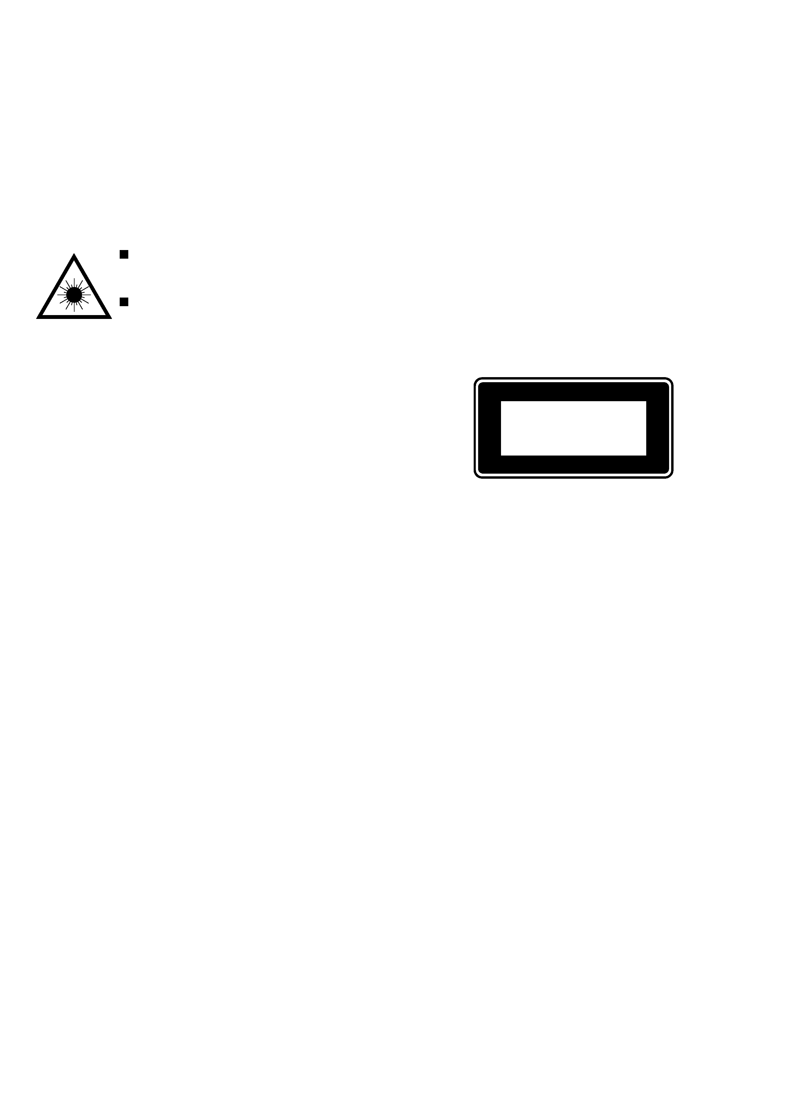
PROTECTION OF EYES FROM LASER BEAM DURING SERVICING
VAROITUS!
Laiteen Käyttäminen muulla kuin tässä käyttöohjeessa mainit-
ulla tavalla saattaa altistaa käyt-täjän turvallisuusluokan 1 ylit-
tävälle näkymättömälle lasersäteilylle.
VARNING!
Om apparaten används på annat sätt än vad som specificeras i
denna bruksanvising, kan användaren utsättas för osynling
laserstrålning, som överskrider gränsen för laserklass 1.
Caution: Invisible laser radiation when
open and interlocks defeated avoid expo-
sure to beam.
Advarsel:Usynling laserståling ved åbning,
når sikkerhedsafbrydere er ude af funktion.
Undgå udsættelse for stråling.
CAUTION
Use of controls or adjustments or performance of procedures
other than those specified herein may result in hazardous
radiation exposure.
ATTENTION
L'utilisation de commandes, réglages ou procédures autres que
ceux spécifiés peut entraîner une dangereuse exposition aux
radiations.
ADVARSEL!
Usynlig laserståling ved åbning, når sikkerhedsafbrydereer ude
af funktion. Undgå udsættelse for stråling.
This Compact Disc player is classified as a CLASS 1 LASER
product.
The CLASS 1 LASER PRODUCT label is located on the rear
exterior.
This set employs laser. Therefore, be sure to follow carefully the
instructions below when servicing.
WARNING!
WHEN SERVICING, DO NOT APPROACH THE LASER EXIT
WITH THE EYE TOO CLOSELY. IN CASE IT IS NECESSARY TO
CONFIRM LASER BEAM EMISSION. BE SURE TO OBSERVE
FROM A DISTANCE OF MORE THAN 30cm FROM THE
SURFACE OF THE OBJECTIVE LENS ON THE OPTICAL
PICK-UP BLOCK.
CLASS 1
KLASSE 1
LUOKAN 1
KLASS 1
LASER PRODUCT
LASER PRODUKT
LASER LAITE
LASER APPARAT